

Page 1

INTEGRATED CIRCUITS
DATA SH EET
SAA6581T
RDS/RBDS demodulator
Product specification
File under Integrated Circuits, IC01
2001 May 07
Page 2

Philips Semiconductors Product specification
RDS/RBDS demodulator SAA6581T
FEATURES
• Integrated switched capacitor filter
• Demodulates European Radio Data System (RDS) or
the USA Radio Broadcast Data System (RBDS) signals
• Oscillator frequencies: 4.332 or 8.664 MHz
• Integrated ARI clamping
• CMOS device
• Single supply voltage: 5 V
• Extended temperature range: −40 to +85 °C
• Low number of external components.
GENERAL DESCRIPTION
The RDS/RBDS demodulator is a CMOS device with
integrated filtering and demodulating of RDS/RBDS
signals comingfrom a multiplexed input data stream. Data
signal RDDA and clock signal RDCL are provided as
outputs for further processing by a suitable
microcomputer, for example CCR921 and CCR922.
The SAA6581T replaces SAA6579 in function and
pin-compatibility.
APPLICATIONS
The RDS/RBDS system offers a large range of
applications from the many functions that can be
implemented. For car radios the most important are:
• Program Service (PS) name
• Traffic Program (TP) identification
• Traffic Announcement (TA) signal
• Alternative Frequency (AF) list
• Program Identification (PI)
• Enhanced Other Networks (EON) information.
QUICK REFERENCE DATA
SYMBOL PARAMETER MIN. TYP. MAX. UNIT
V
DDA
V
DDD
I
DD(tot)
V
i(MPX)
f
i(xtal)
analog supply voltage 4.0 5.0 5.5 V
digital supply voltage 4.0 5.0 5.5 V
total supply current − 6.0 − mA
RDS input sensitivity at pin MPX 1 −−mV
crystal input frequency − 4.332 − MHz
− 8.664 − MHz
ORDERING INFORMATION
TYPE
NUMBER
NAME DESCRIPTION VERSION
PACKAGE
SAA6581T SO16 plastic small outline package; 16 leads; body width 7.5 mm SOT162-1
2001 May 07 2
Page 3

Philips Semiconductors Product specification
RDS/RBDS demodulator SAA6581T
BLOCK DIAGRAM
handbook, full pagewidth
multiplex
input
+5 V
100 nF
330 pF
C2
C1
MPX
V
DDA
4
5
8th ORDER
BANDPASS FILTER
POWER
SUPPLY
AND RESET
6
V
SSAVref
57 kHz
560 pF
C6
87
SAA6581T
TEST
CONTROL
15
TCON
C3
2.2 µF
Fig.1 Block diagram.
CINSCOUT
CLOCKED
COMPARATOR
9
MODE
47 pF
OSCILLATOR
AND CLOCK
13 14
OSCIQ1OSCO
C4
+5 V
V
DDD
12
RDS/RBDS
DEMODULATOR
SIGNAL QUALITY
DETECTOR
C5
56 pF
113
V
SSD
C7
100 nF
10
SYNC
RDCL
16
2
RDDA
1
QUAL
MHB899
2001 May 07 3
Page 4
Philips Semiconductors Product specification
RDS/RBDS demodulator SAA6581T
PINNING
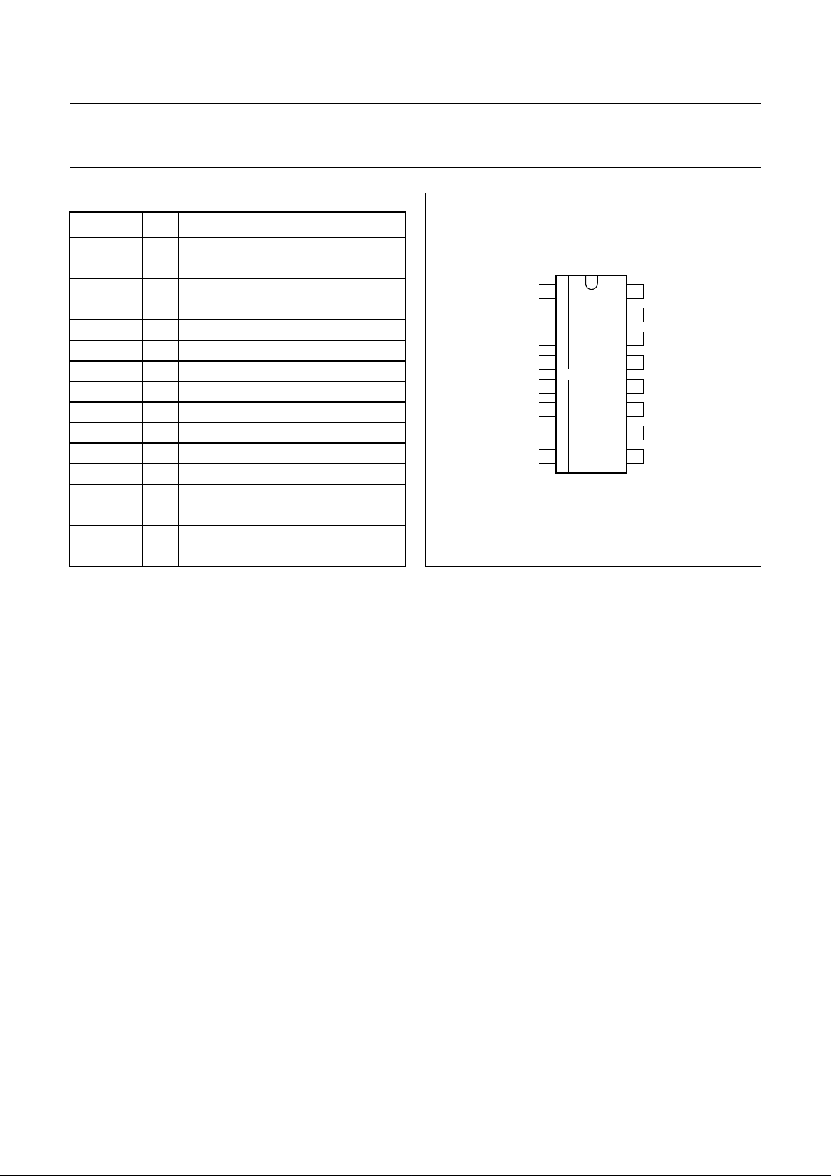
SYMBOL PIN DESCRIPTION
QUAL 1 signal quality indication output
RDDA 2 RDS data output
V
ref
3 reference voltage output (1/2V
MPX 4 multiplex signal input
V
V
DDA
SSA
5 analog supply voltage (5 V)
6 analog ground (0 V)
CIN 7 comparator input
SCOUT 8 switched capacitor filter output
MODE 9 oscillator frequency select input
SYNC 10 ARI clamping control input
V
V
SSD
DDD
11 digital ground (0 V)
12 digital supply voltage (5 V)
OSCI 13 oscillator input
OSCO 14 oscillator output
TCON 15 test control input
RDCL 16 RDS clock output
DDA
)
handbook, halfpage
1
QUAL
2
RDDA
3
V
ref
4
MPX
V
DDA
V
SSA
CIN
SCOUT
SAA6581T
5
6
7
8
MHB900
Fig.2 Pin configuration.
16
15
14
13
12
11
10
9
RDCL
TCON
OSCO
OSCI
V
DDD
V
SSD
SYNC
MODE
FUNCTIONAL DESCRIPTION
RDS/RBDS signal demodulation
BANDPASS FILTER
The bandpass filter has a centre frequency of 57 kHz. It
selects the RDS/RBDSsub-band fromthe multiplex signal
MPX and suppresses the audio signal components. The
filter block contains an analog anti-aliasing filter at the
inputfollowedby an 8thorderswitched capacitor bandpass
filter and a reconstruction filter at the output.
CLOCKED COMPARATOR
Thecomparator digitizestheoutput signalfromthe 57 kHz
bandpass filter for further processing by the digital
RDS/RBDS demodulator. To attain high sensitivity and to
avoid phase distortion, the comparator input stage has
automatic offset compensation.
DEMODULATOR
The demodulator provides all functions of the SAA6579
and improves performance under weak signal conditions.
Demodulator functions include:
• 57 kHz carrier regeneration from the two sidebands
(Costas loop)
• Symbol integration over one RDS clock period
• Bi-phase symbol decoding
• Differential decoding
• Synchronization of RDS/RBDS output data.
The RDS/RBDS demodulator recovers and regenerates
the continuously transmitted RDS/RBDS data stream in
the MPX signal and provides clock RDCL for the output
signalsand dataoutput RDDA forfurther processingby an
RDS/RBDS decoder, for example CCR921 or CCR922.
ARI CLAMP
The demodulator checks the input signal for presence of
RDS only, or RDS plus ARI transmissions. After a fixed
test period, if the SYNC inputis setHIGH the demodulator
locksin the ‘verified’condition(seeTable 1). If SYNCisset
LOW, the ARI clamping is reset (disabled). After SYNC
returns to HIGH, the demodulator resumes checking the
input signal.
2001 May 07 4
Page 5

Philips Semiconductors Product specification
RDS/RBDS demodulator SAA6581T
Table 1 Control pin SYNC
SYNC ARI CLAMPING
LOW internal ARI clamping disabled
HIGH ARI clamping allowed to be logged
SIGNAL QUALITY DETECTION
Output QUAL indicates thesafety ofthe regeneratedRDS
Table 2 Control pins TCON and MODE
TCON MODE OSCILLATOR FREQUENCY
HIGH LOW 4.332 MHz
HIGH HIGH 8.664 MHz
The clock generator generates the internal 4.332 MHz
system clock and timing signal derivatives.
data (HIGH = ‘good’ data; LOW = ‘unsafe’ data).
Power supply and internal reset
Oscillator and system clock generator
For good performance of the bandpass and demodulator
stages, the demodulator requires a crystal oscillator with a
frequency of 4.332 or 8.664 MHz. The demodulator can
operatewith eitherfrequency(see Table 2),so that aradio
set with a microcontroller can run, in this case, with one
crystal only. The demodulator oscillator can drive the
Thedemodulator hasseparate power supplyinputs forthe
digital and analog parts of the device. For the analog
functions an additional reference voltage (1⁄2V
DDA
) is
internally generated and available via the output pin V
The demodulator requires a defined reset condition. The
demodulator generates automatically a reset signal after
the power supplyV
is switched on,or ata voltage-drop.
DDA
microcontroller, or vice versa.
LIMITING VALUES
In accordance with the Absolute Maximum Rating System (IEC 60134).
SYMBOL PARAMETER CONDITIONS MIN. MAX. UNIT
V
DD
V
n
I
i
I
lu(prot)
supply voltage 0 6.5 V
voltage at pins 1 to 4, 7 to 10, and
13 to 16 with respect to pins 6 and 11
inputcurrent atpins 1 to 5, 7 to 11 and
13 to 16
latch-up protection current in pulsed
mode
pins 5 and 12 are
connected to V
DD
pins 6 and 11 are
connected to ground
T
= −40 to +85 °C with
amb
voltage limiting −2 to +10 V
T
=25°C with voltage
amb
−0.5 VDD+ 0.5 ≤ 6.5 V
−10 +10 mA
−100 +100 mA
−200 +200 mA
limiting −2 to +12 V
= −40 to +85 °C
T
amb
−10 +10 mA
without voltage limiting
T
amb
T
stg
V
es
ambient temperature −40 +85 °C
storage temperature −65 +150 °C
electrostatic handling voltage note 1 −4000 +4000 V
note 2 −500 +500 V
ref
.
Notes
1. Human body model (equivalent to discharging a 100 pF capacitor through a 1.5 kΩ series resistor).
2. Machine model (equivalent to discharging a 200 pF capacitor through a0 Ω series resistorand 0.75 µH inductance).
THERMAL CHARACTERISTICS
SYMBOL PARAMETER CONDITIONS VALUE UNIT
R
th(j-a)
thermal resistance from junction to ambient in free air 104 K/W
2001 May 07 5
Page 6

Philips Semiconductors Product specification
RDS/RBDS demodulator SAA6581T
CHARACTERISTICS: DIGITAL PART
V
DDA=VDDD
SYMBOL PARAMETER CONDITIONS MIN. TYP. MAX. UNIT
Supply
V
DDD
I
DDD
P
tot
Inputs
V
IL
V
IH
I
i(pu)
Outputs
V
OL
V
OH
Crystal parameters
f
i(xtal)
∆f
osc
∆f
osc(T)
C
L
R
xtal
=5V; T
=25°C; unless otherwise specified.
amb
digital supply voltage 4.0 5.0 5.5 V
digital supply current − 1.5 − mA
total power dissipation − 30 − mW
LOW-level input voltage at
pins TCON, OSCI, SYNC and
MODE
HIGH-level input voltage at
pins TCON, OSCI, SYNC and
MODE
input pull-up current at
pins TCON and MODE
LOW-level output voltage at
pins QUAL, RDDA and RDCL
HIGH-level output voltage at
pins QUAL, RDDA and RDCL
crystal input frequency TCON = HIGH;
adjustment tolerance of oscillator
frequency
temperature drift of oscillator
frequency
load capacitance − 30 − pF
crystal resonance resistance −−120 Ω
−−0.3V
0.7V
−− V
DDD
DDD
V
VIH= 3.5 V −10 −20 −µA
IOL=2mA −−0.4 V
IOH= −0.02 mA 4.0 −− V
− 4.332 − MHz
MODE = LOW
TCON = HIGH;
− 8.664 − MHz
MODE = HIGH
−−30 × 10
T
= −40 to +85 °C −−30 × 10
amb
−6
−6
2001 May 07 6
Page 7

Philips Semiconductors Product specification
RDS/RBDS demodulator SAA6581T
CHARACTERISTICS: ANALOG PART
V
DDA=VDDD
SYMBOL PARAMETER CONDITIONS MIN. TYP. MAX. UNIT
Supply
V
DDA
V
DDA
I
DD(tot)
V
ref
Z
o(Vref)
MPX input (signal before the capacitor on pin MPX)
V
i(MPX)(rms)
V
i(max)(p-p)
R
i(MPX)
57 kHz bandpass filter
f
c
B
−3dB
G
SCOUT-MPX
α
sb
R
o(SCOUT)
Comparator input (pin CIN)
V
i(min)(rms)
R
i
=5V; T
=25°C; measurements taken in Fig.1; unless otherwise specified.
amb
analog supply voltage 4.0 5.0 5.5 V
− V
difference between analog and
DDD
digital supply voltages
total supply current − 6.0 − mA
reference voltage V
output impedance at pin V
RDS amplitude (RMS value) ∆f=±1.2 kHz RDS-signal;
maximum input signal capability
(peak-to-peak value)
input resistance f = 0 to 100 kHz 40 −−kΩ
centre frequency T
−3 dB bandwidth 2.5 3.0 3.5 kHz
signal gain f = 57 kHz 17 20 23 dB
stop band attenuation ∆f=±7 kHz 31 −−dB
output resistance at pin SCOUT f = 57 kHz − 30 60 Ω
minimum input level
(RMS value)
input resistance 70 110 150 kΩ
ref
− 0 0.5 V
= 5 V 2.25 2.5 2.75 V
DDA
− 25 − kΩ
1 −−mV
∆f=±3.2 kHz ARI-signal
f=57±2 kHz 200 −−mV
f < 50 kHz 1.4 −−V
f < 15 kHz 2.8 −−V
f > 70 kHz 3.5 −−V
= −40 to +85 °C 56.5 57.0 57.5 kHz
amb
f < 45 kHz 40 −−dB
f < 20 kHz 50 −−dB
f > 70 kHz 40 −−dB
f = 57 kHz − 110mV
2001 May 07 7
Page 8

Philips Semiconductors Product specification
RDS/RBDS demodulator SAA6581T
TIMING DATA
handbook, full pagewidth
RDCL
RDDA
t
d(clk)
t
CLKH
Table 3 RDS timing (see Fig.3)
SYMBOL PARAMETER TYP. UNIT
t
d(clk)
T
CLK
t
CLKH
T
bit(slipped)
clock-data delay 4 µs
clock period 842 µs
clock HIGH time 421 µs
slipped data bit period 1263 µs
t
T
CLK
T
bit(slipped)
d(clk)
Fig.3 RDS timing diagram including a phase change.
MHB901
2001 May 07 8
Page 9

Philips Semiconductors Product specification
RDS/RBDS demodulator SAA6581T
PACKAGE OUTLINE
SO16: plastic small outline package; 16 leads; body width 7.5 mm
D
c
y
Z
16
pin 1 index
1
e
9
A
2
A
8
w M
b
p
SOT162-1
E
H
E
Q
1
L
p
L
detail X
(A )
A
X
v M
A
A
3
θ
0 5 10 mm
scale
DIMENSIONS (inch dimensions are derived from the original mm dimensions)
mm
OUTLINE
VERSION
SOT162-1
A
max.
2.65
0.10
A
0.30
0.10
0.012
0.004
A2A
1
2.45
2.25
0.096
0.089
IEC JEDEC EIAJ
075E03 MS-013
0.25
0.01
b
3
p
0.49
0.32
0.36
0.23
0.019
0.013
0.014
0.009
UNIT
inches
Note
1. Plastic or metal protrusions of 0.15 mm maximum per side are not included.
(1)E(1) (1)
cD
10.5
7.6
10.1
7.4
0.41
0.30
0.29
0.050
0.40
REFERENCES
2001 May 07 9
eHELLpQ
1.27
10.65
10.00
0.419
0.394
1.4
0.055
1.1
0.4
0.043
0.016
1.1
1.0
0.043
0.039
0.25
0.25 0.1
0.01
0.01
EUROPEAN
PROJECTION
ywv θ
Z
0.9
0.4
8
0.004
ISSUE DATE
0.035
0.016
97-05-22
99-12-27
0
o
o
Page 10

Philips Semiconductors Product specification
RDS/RBDS demodulator SAA6581T
SOLDERING
Introduction to soldering surface mount packages
Thistext gives averybrief insight toa complex technology.
A more in-depth account of soldering ICs can be found in
our
“Data Handbook IC26; Integrated Circuit Packages”
(document order number 9398 652 90011).
There is no soldering method that is ideal for all surface
mount IC packages. Wave soldering can still be used for
certainsurface mount ICs,butit is notsuitablefor fine pitch
SMDs. In these situations reflow soldering is
recommended.
Reflow soldering
Reflow soldering requires solder paste (a suspension of
fine solder particles, flux and binding agent) to be applied
tothe printed-circuitboardby screenprinting,stencilling or
pressure-syringe dispensing before package placement.
Several methods exist for reflowing; for example,
convection or convection/infrared heating in a conveyor
type oven. Throughput times (preheating, soldering and
cooling) vary between 100 and 200 seconds depending
on heating method.
Typical reflow peak temperatures range from
215 to 250 °C. The top-surface temperature of the
packages should preferable be kept below 220 °C for
thick/large packages, and below 235 °C for small/thin
packages.
Wave soldering
Conventional single wave soldering is not recommended
forsurface mount devices(SMDs)or printed-circuit boards
with a high component density, as solder bridging and
non-wetting can present major problems.
To overcome these problems the double-wave soldering
method was specifically developed.
If wave soldering is used the following conditions must be
observed for optimal results:
• Use a double-wave soldering method comprising a
turbulent wavewith high upwardpressure followed bya
smooth laminar wave.
• For packages with leads on two sides and a pitch (e):
– larger than or equal to 1.27 mm, the footprint
longitudinal axis is preferred to be parallel to the
transport direction of the printed-circuit board;
– smaller than 1.27 mm, the footprint longitudinal axis
must be parallel to the transport direction of the
printed-circuit board.
The footprint must incorporate solder thieves at the
downstream end.
• Forpackages with leadsonfour sides, thefootprintmust
be placedat a 45° angle to the transport direction of the
printed-circuit board. The footprint must incorporate
solder thieves downstream and at the side corners.
During placement and before soldering, the package must
be fixed with a droplet of adhesive. The adhesive can be
applied by screen printing, pin transfer or syringe
dispensing. The package can be soldered after the
adhesive is cured.
Typical dwell time is 4 seconds at 250 °C.
A mildly-activated flux will eliminate the need for removal
of corrosive residues in most applications.
Manual soldering
Fix the component by first soldering two
diagonally-opposite end leads. Use a low voltage (24 V or
less) soldering iron applied to the flat part of the lead.
Contact time must be limited to 10 seconds at up to
300 °C.
When using a dedicated tool, all other leads can be
soldered in one operation within 2 to 5 seconds between
270 and 320 °C.
2001 May 07 10
Page 11

Philips Semiconductors Product specification
RDS/RBDS demodulator SAA6581T
Suitability of surface mount IC packages for wave and reflow soldering methods
PACKAGE
WAVE REFLOW
(1)
BGA, HBGA, LFBGA, SQFP, TFBGA not suitable suitable
SOLDERING METHOD
HBCC, HLQFP, HSQFP, HSOP, HTQFP, HTSSOP, HVQFN, SMS not suitable
(3)
PLCC
, SO, SOJ suitable suitable
LQFP, QFP, TQFP not recommended
SSOP, TSSOP, VSO not recommended
(2)
(3)(4)
(5)
suitable
suitable
suitable
Notes
1. All surface mount (SMD) packages are moisture sensitive. Depending upon the moisture content, the maximum
temperature (with respect to time) and body size of the package, there is a risk that internal or external package
cracks may occur due to vaporization of the moisture in them (the so called popcorn effect). For details, refer to the
Drypack information in the
“Data Handbook IC26; Integrated Circuit Packages; Section: Packing Methods”
.
2. These packages are not suitable for wave soldering as a solder joint between the printed-circuit board and heatsink
(at bottom version) can not be achieved, and as solder may stick to the heatsink (on top version).
3. If wave soldering is considered, then the package must be placed at a 45° angle to the solder wave direction.
The package footprint must incorporate solder thieves downstream and at the side corners.
4. Wave soldering is only suitable for LQFP, TQFP and QFP packages with a pitch (e) equal to or larger than 0.8 mm;
it is definitely not suitable for packages with a pitch (e) equal to or smaller than 0.65 mm.
5. Wave soldering is onlysuitable for SSOP and TSSOPpackages with a pitch (e) equal toor larger than 0.65 mm; it is
definitely not suitable for packages with a pitch (e) equal to or smaller than 0.5 mm.
2001 May 07 11
Page 12

Philips Semiconductors Product specification
RDS/RBDS demodulator SAA6581T
DATA SHEET STATUS
PRODUCT
DATA SHEET STATUS
Objective data Development This data sheet contains data from the objective specification for product
Preliminary data Qualification This data sheet contains data from the preliminary specification.
Product data Production This data sheet contains data from the product specification. Philips
(1)
STATUS
(2)
DEFINITIONS
development. Philips Semiconductors reserves the right to change the
specification in any manner without notice.
Supplementary data will be published at a later date. Philips
Semiconductors reserves the right to change the specification without
notice, in order to improve the design and supply the best possible
product.
Semiconductors reserves the right to make changes at any time in order
to improve the design, manufacturing and supply. Changes will be
communicated according to the Customer Product/Process Change
Notification (CPCN) procedure SNW-SQ-650A.
Notes
1. Please consult the most recently issued data sheet before initiating or completing a design.
2. The product status of the device(s) described in this data sheet may have changed since this data sheet was
published. The latest information is available on the Internet at URL http://www.semiconductors.philips.com.
DEFINITIONS
Short-form specification The data in a short-form
specification is extracted from a full data sheet with the
same type number and title. For detailed information see
the relevant data sheet or data handbook.
Limiting values definition Limiting valuesgiven are in
accordance with the Absolute Maximum Rating System
(IEC 60134). Stress above one or more of the limiting
values may cause permanent damage to the device.
These are stress ratings only and operation of the device
atthese or atany other conditionsabovethose given inthe
Characteristics sectionsof the specification is not implied.
Exposure to limiting values for extended periods may
affect device reliability.
Application information Applications that are
described herein for any of these products are for
illustrative purposes only. Philips Semiconductors make
norepresentation or warrantythat suchapplicationswill be
suitable for the specified use without further testing or
modification.
DISCLAIMERS
Life support applications These products are not
designed for use in life support appliances, devices, or
systems where malfunction of these products can
reasonably be expectedto resultin personalinjury. Philips
Semiconductorscustomers using orselling theseproducts
for use in such applications do so at their own risk and
agree to fully indemnify Philips Semiconductors for any
damages resulting from such application.
Right to make changes Philips Semiconductors
reserves the right to make changes, without notice, in the
products, including circuits, standard cells, and/or
software, described or contained herein in order to
improve design and/or performance. Philips
Semiconductors assumes no responsibility or liability for
theuse of anyofthese products, conveysnolicence or title
under any patent, copyright, or mask work right to these
products,and makes norepresentations or warrantiesthat
these products are free from patent, copyright, or mask
work right infringement, unless otherwise specified.
2001 May 07 12
Page 13

Philips Semiconductors Product specification
RDS/RBDS demodulator SAA6581T
NOTES
2001 May 07 13
Page 14

Philips Semiconductors Product specification
RDS/RBDS demodulator SAA6581T
NOTES
2001 May 07 14
Page 15

Philips Semiconductors Product specification
RDS/RBDS demodulator SAA6581T
NOTES
2001 May 07 15
Page 16

Philips Semiconductors – a w orldwide compan y
Argentina: see South America
Australia: 3 Figtree Drive, HOMEBUSH, NSW 2140,
Tel. +61 2 9704 8141, Fax. +61 2 9704 8139
Austria: Computerstr. 6, A-1101 WIEN, P.O. Box 213,
Tel. +43 1 60 101 1248, Fax. +43 1 60 101 1210
Belarus: Hotel Minsk Business Center, Bld. 3, r. 1211, Volodarski Str. 6,
220050 MINSK, Tel. +375 172 20 0733, Fax. +375 172 20 0773
Belgium: see The Netherlands
Brazil: see South America
Bulgaria: Philips Bulgaria Ltd., Energoproject, 15th floor,
51 James Bourchier Blvd., 1407 SOFIA,
Tel. +359 2 68 9211, Fax. +359 2 68 9102
Canada: PHILIPS SEMICONDUCTORS/COMPONENTS,
Tel. +1 800 234 7381, Fax. +1 800 943 0087
China/Hong Kong: 501 Hong Kong Industrial Technology Centre,
72 Tat Chee Avenue, Kowloon Tong, HONG KONG,
Tel. +852 2319 7888, Fax. +852 2319 7700
Colombia: see South America
Czech Republic: see Austria
Denmark: Sydhavnsgade 23, 1780 COPENHAGEN V,
Tel. +45 33 29 3333, Fax. +45 33 29 3905
Finland: Sinikalliontie 3, FIN-02630 ESPOO,
Tel. +358 9 615 800, Fax. +358 9 6158 0920
France: 7 - 9 Rue du Mont Valérien, BP317, 92156 SURESNES Cedex,
Tel. +33 1 4728 6600, Fax. +33 1 4728 6638
Germany: Hammerbrookstraße 69, D-20097 HAMBURG,
Tel. +49 40 2353 60, Fax. +49 40 2353 6300
Hungary: Philips Hungary Ltd., H-1119 Budapest, Fehervari ut 84/A,
Tel: +36 1 382 1700, Fax: +36 1 382 1800
India: Philips INDIA Ltd, Band Box Building, 2nd floor,
254-D, Dr. Annie Besant Road, Worli, MUMBAI 400 025,
Tel. +91 22 493 8541, Fax. +91 22 493 0966
Indonesia: PT Philips Development Corporation, Semiconductors Division,
Gedung Philips, Jl. Buncit Raya Kav.99-100, JAKARTA 12510,
Tel. +62 21 794 0040 ext. 2501, Fax. +62 21 794 0080
Ireland: Newstead, Clonskeagh, DUBLIN 14,
Tel. +353 1 7640 000, Fax. +353 1 7640 200
Israel: RAPAC Electronics, 7 Kehilat Saloniki St, PO Box 18053,
TEL AVIV 61180, Tel. +972 3 645 0444, Fax. +972 3 649 1007
Italy: PHILIPS SEMICONDUCTORS, Via Casati, 23 - 20052 MONZA (MI),
Tel. +39 039 203 6838, Fax +39 039 203 6800
Japan: Philips Bldg 13-37, Kohnan 2-chome, Minato-ku,
TOKYO 108-8507, Tel. +81 3 3740 5130, Fax. +81 3 3740 5057
Korea: Philips House, 260-199 Itaewon-dong, Yongsan-ku, SEOUL,
Tel. +82 2 709 1412, Fax. +82 2 709 1415
Malaysia: No. 76 Jalan Universiti, 46200 PETALING JAYA, SELANGOR,
Tel. +60 3 750 5214, Fax. +60 3 757 4880
Mexico: 5900 Gateway East, Suite 200, EL PASO, TEXAS 79905,
Tel. +9-5 800 234 7381, Fax +9-5 800 943 0087
Middle East: see Italy
Netherlands: Postbus 90050, 5600 PB EINDHOVEN, Bldg. VB,
Tel. +31 40 27 82785, Fax. +31 40 27 88399
New Zealand: 2 Wagener Place, C.P.O. Box 1041, AUCKLAND,
Tel. +64 9 849 4160, Fax. +64 9 849 7811
Norway: Box 1, Manglerud 0612, OSLO,
Tel. +47 22 74 8000, Fax. +47 22 74 8341
Pakistan: see Singapore
Philippines: Philips Semiconductors Philippines Inc.,
106 Valero St. Salcedo Village, P.O. Box 2108 MCC, MAKATI,
Metro MANILA, Tel. +63 2 816 6380, Fax. +63 2 817 3474
Poland: Al.Jerozolimskie 195 B, 02-222 WARSAW,
Tel. +48 22 5710 000, Fax. +48 22 5710 001
Portugal: see Spain
Romania: see Italy
Russia: Philips Russia, Ul. Usatcheva 35A, 119048 MOSCOW,
Tel. +7 095 755 6918, Fax. +7 095 755 6919
Singapore: Lorong 1, Toa Payoh, SINGAPORE 319762,
Tel. +65 350 2538, Fax. +65 251 6500
Slovakia: see Austria
Slovenia: see Italy
South Africa: S.A. PHILIPS Pty Ltd., 195-215 Main Road Martindale,
2092 JOHANNESBURG, P.O. Box 58088 Newville 2114,
Tel. +27 11 471 5401, Fax. +27 11 471 5398
South America: Al. Vicente Pinzon, 173, 6th floor,
04547-130 SÃO PAULO, SP, Brazil,
Tel. +55 11 821 2333, Fax. +55 11 821 2382
Spain: Balmes 22, 08007 BARCELONA,
Tel. +34 93 301 6312, Fax. +34 93 301 4107
Sweden: Kottbygatan 7, Akalla, S-16485 STOCKHOLM,
Tel. +46 8 5985 2000, Fax. +46 8 5985 2745
Switzerland: Allmendstrasse 140, CH-8027 ZÜRICH,
Tel. +41 1 488 2741 Fax. +41 1 488 3263
Taiwan: Philips Semiconductors, 5F, No. 96, Chien Kuo N. Rd., Sec. 1,
TAIPEI, Taiwan Tel. +886 2 2134 2451, Fax. +886 2 2134 2874
Thailand: PHILIPS ELECTRONICS (THAILAND) Ltd.,
60/14 MOO 11, Bangna Trad Road KM. 3, Bagna, BANGKOK 10260,
Tel. +66 2 361 7910, Fax. +66 2 398 3447
Turkey: Yukari Dudullu, Org. San. Blg., 2.Cad. Nr. 28 81260 Umraniye,
ISTANBUL, Tel. +90 216 522 1500, Fax. +90 216 522 1813
Ukraine: PHILIPS UKRAINE, 4 Patrice Lumumba str., Building B, Floor 7,
252042 KIEV, Tel. +380 44 264 2776, Fax. +380 44 268 0461
United Kingdom: Philips Semiconductors Ltd., 276 Bath Road, Hayes,
MIDDLESEX UB3 5BX, Tel. +44 208 730 5000, Fax. +44 208 754 8421
United States: 811 East Arques Avenue, SUNNYVALE, CA 94088-3409,
Tel. +1 800 234 7381, Fax. +1 800 943 0087
Uruguay: see South America
Vietnam: see Singapore
Yugoslavia: PHILIPS, Trg N. Pasica 5/v, 11000 BEOGRAD,
Tel. +381 11 3341 299, Fax.+381 11 3342 553
For all other countries apply to: Philips Semiconductors,
Marketing Communications, Building BE-p, P.O. Box 218, 5600 MD EINDHOVEN,
The Netherlands, Fax. +31 40 27 24825
© Philips Electronics N.V. SCA
All rights are reserved. Reproduction in whole or in part is prohibited without the prior written consent of the copyright owner.
The information presented in this document does not form part of any quotation or contract, is believed to be accurate and reliable and may be changed
without notice. No liability will be accepted by the publisher for any consequence of its use. Publication thereof does not convey nor imply any license
under patent- or other industrial or intellectual property rights.
2001
Internet: http://www.semiconductors.philips.com
72
Printed in The Netherlands 753503/01/pp16 Date of release: 2001 May 07 Document order number: 9397 750 08148
 Loading...