

Page 1
INTEGRATED CIRCUITS
DATA SH EET
SAA2501
Digital Audio Broadcast (DAB)
decoder
Preliminary specification
File under Integrated Circuits, IC01
Philips Semiconductors
January 1995
Page 2

Philips Semiconductors Preliminary specification
Digital Audio Broadcast (DAB) decoder SAA2501
CONTENTS
FEATURES
2 APPLICATION
3 GENERAL DESCRIPTION
4 ORDERING INFORMATION
5 BLOCK DIAGRAM
6 PINNING
7 FUNCTIONAL DESCRIPTION
7.1 Coding system
7.2 Basic functionality
7.3 SAA2501 clocks
7.4 Crystal oscillator
7.5 Clock frequencies when using the slave input
7.6 Clock frequencies when using the master input
7.7 Target applications; applying the SAA2501 with
2 ISO/MPEG sources
7.8 Buffered clock outputs
7.9 Functionality issues
7.10 Synchronization to input data bitstreams
7.11 Master input bit rate selection
7.12 Sample rate selection
7.13 Handling of errors in the coded input data
7.14 sub-band filter signals
7.15 Baseband audio processing
7.16 Decoding control signals
7.17 Coded data interfaces
7.17.1 The coded data master input interface
7.17.2 The coded data slave input interface
7.17.3 Slave input transfer speed of first frame
7.17.4 Slave input transfer speed of subsequent
frames
7.18 The sub-band filter interface
7.19 The baseband output interface
7.20 The L3 control interface
7.20.1 L3 signals
7.20.2 L3 transfer types
7.20.3 L3 interface initialization at an SAA2501 device
reset
7.20.4 L3 interface control
7.20.5 SAA2501 status
7.20.6 Data items
7.20.6.1 General data items
7.20.7 SAA2501 settings item
7.20.8 Input data frame header items
7.20.9 Error report item
7.20.10 Audio service synchronized data item
7.20.11 Ancillary Data/XPAD item
7.20.12 APU coefficients item
7.20.13 Speed limitations of the L3 interface
7.20.14 Default item data values after reset
8 APPENDIX
8.1 Preliminary specification 3-line ‘L3’ interface
8.1.1 Introduction
8.1.1.1 Addressing mode
8.1.1.2 Special function operational address
8.1.1.3 Data mode
8.1.1.4 Halt mode
8.1.2 Device interface reset
8.1.3 Extended addressing
8.1.3.1 Operational address declaration
8.1.3.2 Operational address invalidation
8.1.4 Example of a data transfer
8.1.5 Timing requirements
8.1.5.1 Addressing mode
8.1.5.2 Data mode
8.1.5.3 Halt mode
8.2 SAA2501 L3 protocol enhancement options
8.2.1 Testing L3RDY by polling L3DATA
8.2.2 Options to increase the timing accuracy of the
APU coefficient writing
9 LIMITING VALUES
10 DC CHARACTERISTICS
11 AC CHARACTERISTICS
12 APPLICATION INFORMATION
13 PACKAGE OUTLINE
14 SOLDERING
14.1 Plastic quad flat-packs
14.1.1 By wave
14.1.2 By solder paste reflow
14.1.3 Repairing soldered joints (by hand-held
soldering iron or pulse-heated solder tool)
15 DEFINITIONS
16 LIFE SUPPORT APPLICATIONS
January 1995 2
Page 3

Philips Semiconductors Preliminary specification
Digital Audio Broadcast (DAB) decoder SAA2501
1 FEATURES
• Advanced error protection
• Integrated audio post processing for control of signal
level and inter-channel crosstalk
• Demultiplexing of Program Associated Data (PAD) in
the input bitstream
• Automatic digital de-emphasis of the decoded
audio signal
• Separate master and slave inputs
• Automatic sample frequency and bit-rate switching in
master input mode
• Automatic synchronization of input and output interface
clocks in master input mode
• Selectable audio output precision; 16, 18, 20 or 22 bit
• Low power consumption
• Decoded sub-band signal and error flag outputs for error
concealment.
4 ORDERING INFORMATION
TYPE NUMBER
SAA2501H QFP44
NAME DESCRIPTION VERSION
(1)
plastic quad flat package; 44 leads (lead length 1.3 mm);
body 10 × 10 × 1.75 mm
2 APPLICATION
• Digital Audio Broadcast systems as defined in
“Eureka 147”
3 GENERAL DESCRIPTION
The SAA2501 audio source decoder supports ISO/IEC
MPEG layers I and II and all DAB specific features as
described in
PACKAGE
.
“Eureka 147 draft specification (EU147)”
SOT307-2
.
Note
1. When using IR reflow soldering it is recommended that the Drypack instructions in the
(order number 9398 510 63011) are followed.
Supply of this
right under any patent, or any Industrial or Intellectual Property Right, to use this IC in any ready-to-use
electronic product.
“ISO/IEC 11172-3”
audio standard Layer I or layer II compatible IC does not convey a licence nor imply a
“Quality Reference Handbook”
January 1995 3
Page 4
Philips Semiconductors Preliminary specification
Digital Audio Broadcast (DAB) decoder SAA2501
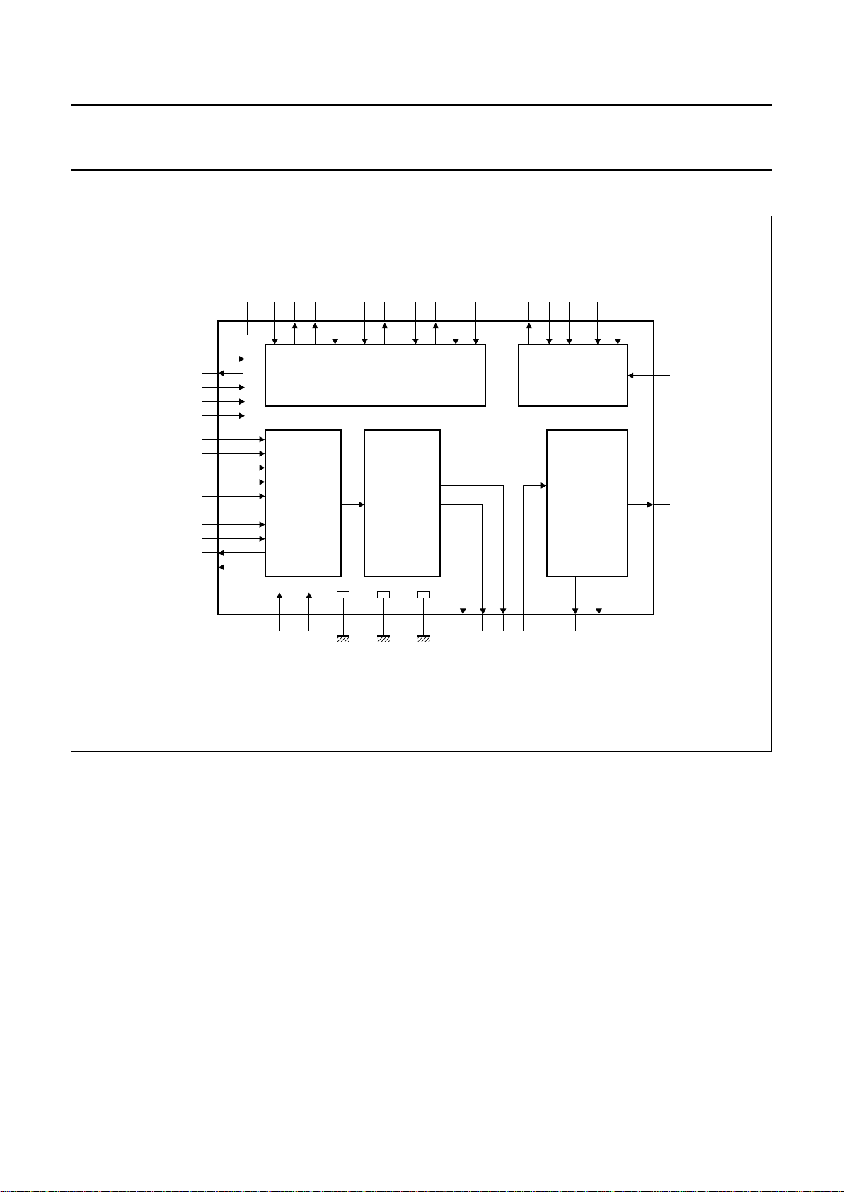
5 BLOCK DIAGRAM
handbook, full pagewidth
CDSEF
CDSCL
CDSWA
CDSSY
CDMEF
CDMCL
CDMWS
TDI
TDO
TCK
TMS
TRST
CDS
CDM
DD1
V
534
41
37
39
40
38
19
20
18
21
22
15
14
16
13
DD2
V
PROCESSOR
TC0 TC1
MCLK
MCLKIN
MCLKOUT
7444 10 9 3242 43 24 25 23 11 12
8
X22IN
MCLK24
CLOCK
GENERATOR
X22OUT
FSCLK
FSCLKIN
FSCLKM
FSCLK384
L3DATA
L3MODE
DECODING
CONTROL
L3CLK
SAA2501
SYNTHESYS
SUBBAND
FILTER
BANK
AND
OUTPUT
PROCESSING
SCK WS
FDAI
INPUT
36 35
PROCESSOR
17
GND2
DEQUANTI-
ZATION
AND
SCALING
GND3
6
GND1
FDEF
FDAO
FDFSY
URDA
STOP
1
RESET
26
SD
29 303231332728
MBE112
Fig.1 Functional block diagram.
January 1995 4
Page 5

Philips Semiconductors Preliminary specification
Digital Audio Broadcast (DAB) decoder SAA2501
6 PINNING
SYMBOL PIN DESCRIPTION TYPE
RESET 1 master reset input I
FSCLK 2 sample rate clock output; buffered signal O
FSCLKIN 3 sample rate clock signal input (see Table 1) I
MCLK 4 master clock output; buffered signal O
V
DD1
GND1 6 ground 1 −
MCLKOUT 7 master clock oscillator output O
MCLKIN 8 master clock oscillator input or signal input I
X22OUT 9 22.579 MHz clock oscillator output O
X22IN 10 22.579 MHz clock oscillator input or signal input I
STOP 11 stop decoding input I
URDA 12 unreliable data input; interrupt decoding I
CDMWS 13 coded data (master input) word select output O
CDMEF 14 coded data (master input) error flag input I
CDM 15 ISO/MPEG coded data (master input) I
CDMCL 16 coded data (master input) bit clock output O
GND2 17 ground 2 −
CDSCL 18 coded data (slave input) bit clock I
CDS 19 ISO/MPEG or EU147 (see Table 8) coded data (slave input) I
CDSEF 20 coded data (slave input) error flag I
CDSWA 21 coded data (slave input) burst window signal I
CDSSY 22 coded data (slave input) frame sync I
L3CLK 23 L3 interface bit clock input I
L3DATA 24 L3 interface serial data input/output I/O
L3MODE 25 L3 interface address/data select input I
SD 26 baseband audio I
FDEF 27 filter data error flag output O
GND3 28 ground 3 −
SCK 29 baseband audio data I
WS 30 baseband audio data I
FDAO 31 filter data output O
FDAI 32 filter data input I
FDFSY 33 filter data output frame sync O
V
DD2
TC1 35 do not connect; factory test control 1 input, with integrated pull-down resistor I
TC0 36 do not connect; factory test control 0 input, with integrated pull-down resistor I
TDO 37 boundary scan test data output O
TRST 38 boundary scan test reset input; this pin should be connected to ground for
TCK 39 boundary scan test clock input I
5 supply voltage 1 −
2
S data output O
2
S clock output O
2
S word select output O
34 supply voltage 2 −
normal operation
I
January 1995 5
Page 6
Philips Semiconductors Preliminary specification
Digital Audio Broadcast (DAB) decoder SAA2501
SYMBOL PIN DESCRIPTION TYPE
TMS 40 boundary scan test mode select input I
TDI 41 boundary scan test data input I
FSCLK384 42 sample rate clock frequency indication input I
FSCLKM 43 sample rate clock source selection for the master input I
MCLK24 44 master clock frequency indication input I
dbook, full pagewidth
1
2
3
4
5
6
7
8
9
10
11
12
13
14
15
16
17
18
21
19
20
33
32
31
30
29
28
27
26
25
24
23
22
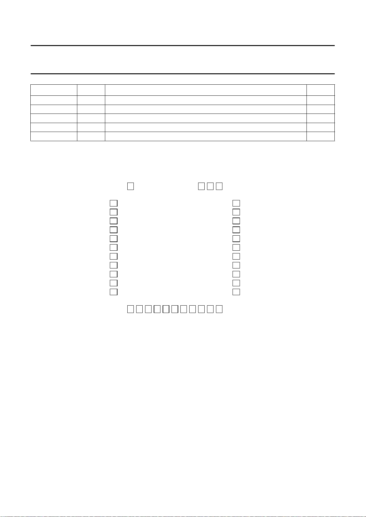
Fig.2 Pin configuration (QFP44).
January 1995 6
 Loading...