

Page 1
INTEGRATED CIRCUITS
DATA SH EET
SAA2023
Drive processor for DCC systems
Preliminary specification
File under Integrated Circuits, IC01
Philips Semiconductors
May 1994
Page 2
Philips Semiconductors Preliminary specification
Drive processor for DCC systems SAA2023
FEATURES
• Operating supply voltage: 4.5 to 5.5 V
• Low power dissipation: 260 mW at 5.0 V
• Single chip digital equalizer, tape formatting and error
correction
• 8-bit flash analog-to-digital converter (ADC) for low
symbol error rate
• Two switchable Infinite Impulse-Response (IIR) filter
sections
• 10-tap Finite Impulse-Response (FIR) filter per main
data channel, with 8 bit coefficients, identical for all main
channels
• 10-tap FIR filter for the AUX channel
• Analog and digital eye outputs
• Interrupt line triggered by internal auxiliary envelope
processing e.g. label, counter, and others
• Robust programmable digital PLL clock extraction unit
• Low power SLEEP mode
• Slew rate limited Electromagnetic Compatibility (EMC)
friendly output
• Digital Compact Cassette (DCC) optimized error
correction
• Programmable symbol synchronization strategy for tape
input data
• Microcontroller control of capstan servo possible during
playback and recording
• Frequency and phase regulation of capstan servo
during playback
• Choice of Dynamic Random Access Memory (DRAM)
and Static Random Access Memory (SRAM) types for
system Random Access Memory (RAM)
• Scratch pad RAM for microcontroller in system RAM
• Integrated interface for Precision Adaptive Sub-band
Coding (PASC) data bus
• Three wire microcontroller ‘L3’ interface
• Protection against invalid auxiliary data
• Seamless joins between recordings.
GENERAL DESCRIPTION
The SAA2023 performs the drive processor function in the
DCC system. This function is built up of digital equalizer,
error correction and tape formatting functions. The digital
equalizer is intended for use with DCC read amplifiers
TDA1318 or TDA1380. The tape formatting and error
correction circuit is intended for use with PASC ICs
SAA2003 and SAA2013, and write amplifiers TDA1319 or
TDA1381.
ORDERING INFORMATION
TYPE NUMBER
SAA2023H 80 TQFP80
SAA2023GP 80 QFP80
Note
1. When using reflow soldering it is recommended that the Dry Packing instructions in the
Pocketbook”
May 1994 2
are followed. The pocketbook can be ordered using the code 9398 510 34011.
PACKAGE
PINS PIN POSITION MATERIAL CODE
(1)
(1)
plastic SOT315-1
plastic SOT318-2
“Quality Reference
Page 3
Philips Semiconductors Preliminary specification
Drive processor for DCC systems SAA2023
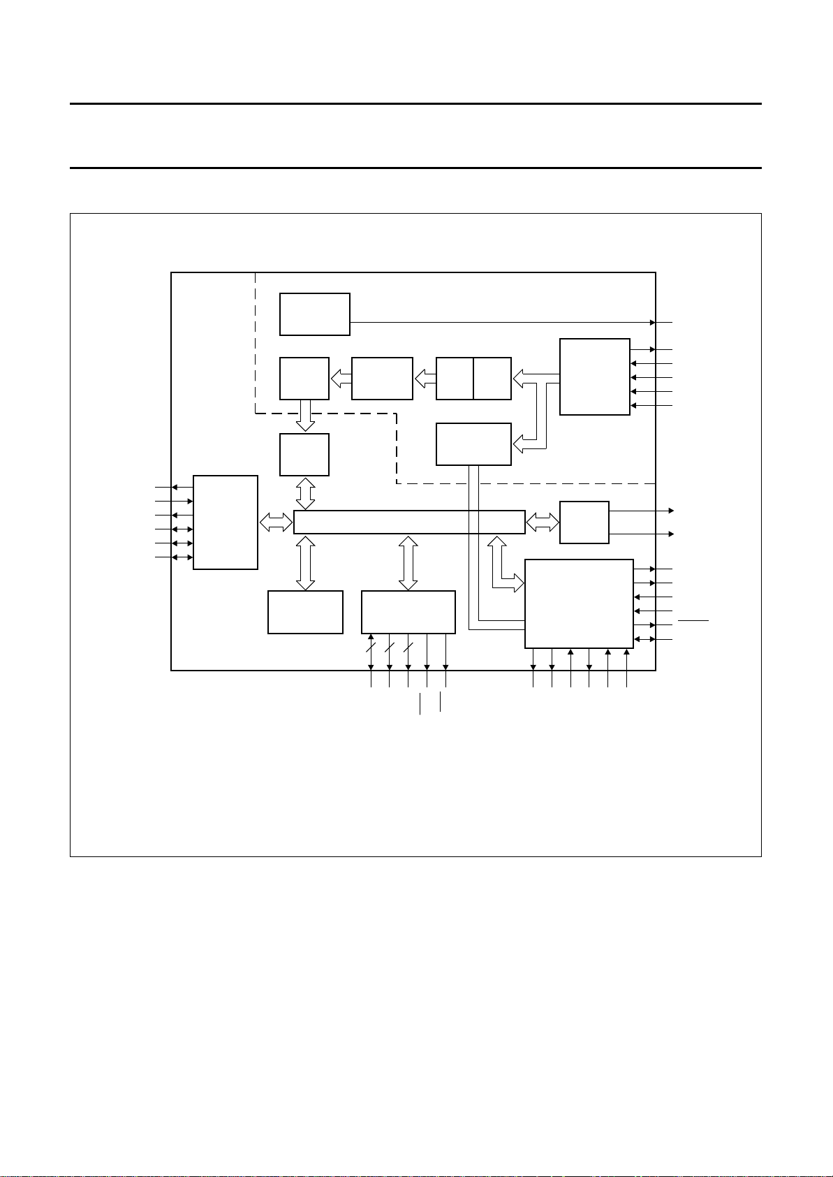
BLOCK DIAGRAM
handbook, full pagewidth
SBDIR
SBMCLK
SBEF
SBDA
SBCL
SBWS
SAA2023
SUB-BAND
2
I S
INTERFACE
DIGITAL-
TO-ANALOG
CONVERTER
PHASE
LOCKED
LOOP
TAPE
INPUT
BUFFER
ERROR
CORRECTOR
ZERO
CROSSING
INTERNAL DATA BUS
RAM
INTERFACE
8116
(1)
FIR
IIR
AUXILIARY
ENVELOPE
DETECTION
ANAEYE
RDSYNC
(2)
ANALOG
TO-DIGITAL
CONVERTER
EQUALIZER
MODULE
TAPE
OUTPUT
BUFFER
CONTROL
INTERFACE
RDMUX
BIAS
V
ref(p)
V
ref(n)
TCLOCK
WDATA
SPEED
URDA
RESET
SLEEP
L3REF
L3DATA
(1) FIR = Finite Impulse-Response.
(2) IIR = Infinite Impulse-Response.
OEN
WEN
D0 to D7
A0 to A10
A11 to A16
Fig.1 Block diagram.
PINO1
PINO2
PINI
L3INT
L3CLK
L3MODE
MGB378
May 1994 3
Page 4
Philips Semiconductors Preliminary specification
Drive processor for DCC systems SAA2023
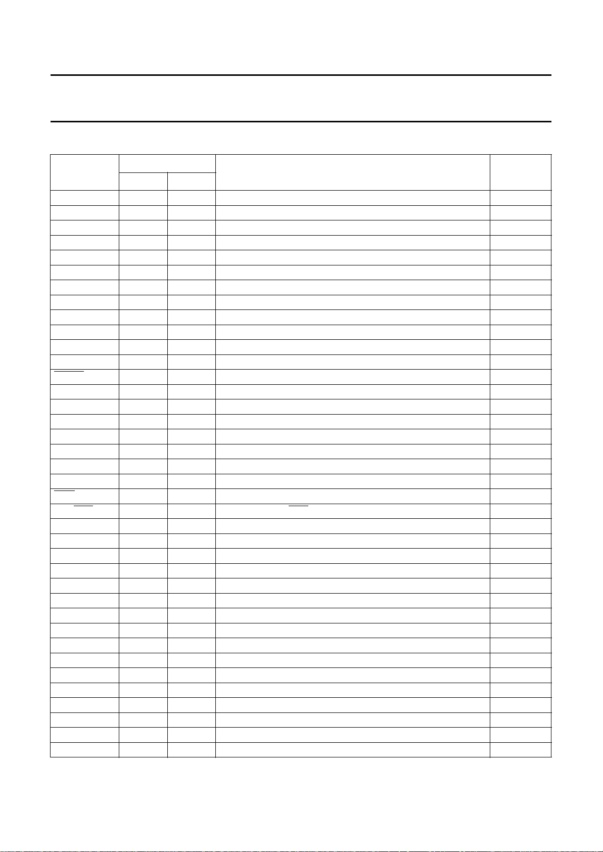
PINNING
SYMBOL
PIN
DESCRIPTION TYPE
(1)
QFP80 TQFP80
SBWS 1 79 word select for sub-band PASC interface I/O (1 mA)
SBCL 2 80 bit clock for sub-band PASC interface I/O (1 mA)
SBDA 3 1 data line for sub-band PASC interface I/O (1 mA)
SBDIR 4 2 direction line for sub-band PASC interface O (1 mA)
SBMCLK 5 3 master clock for sub-band PASC interface I
URDA 6 4 unreliable data O (1 mA)
L3MODE 7 5 mode line for L3 interface I
L3CLK 8 6 bit clock line for L3 interface I
L3DATA 9 7 serial data line for L3 interface I/O (2 mA)
L3INT 10 8 L3 interrupt output O (1 mA)
V
V
DD1
SS1
11 9 digital supply voltage S
12 10 digital ground S
L3REF 13 11 L3 bus timing reference O (1 mA)
RESET 14 12 reset SAA2023 I
SLEEP 15 13 sleep mode selection of SAA2023 I
CLK24 16 14 24.576 MHz clock input I
AZCHK 17 15 channel 0 and channel 7 azimuth monitor O (1 mA)
MCLK 18 16 6.144 MHz clock output O (1 mA)
TEST3 19 17 TEST3 output; do not connect O (1 mA)
ERCOSTAT 20 18 ERCO status, for symbol error rate measurements O (1 mA)
OEN 21 19 output enable for RAM O (2 mA)
RAS 22 20 address SRAM; RAS DRAM O (2 mA)
A10/
V
V
DD2
SS2
23 21 digital supply voltage S
24 22 digital ground S
D7 25 23 data SRAM I/O (4 mA)
D6 26 24 data SRAM I/O (4 mA)
D5 27 25 data SRAM I/O (4 mA)
D4 28 26 data SRAM I/O (4 mA)
D3 29 27 data SRAM; data DRAM I/O (4 mA)
D2 30 28 data SRAM; data DRAM I/O (4 mA)
D1 31 29 data SRAM; data DRAM I/O (4 mA)
V
V
DD7
SS7
32 30 digital supply voltage for RAM S
33 31 digital ground for RAM S
D0 34 32 data SRAM; data DRAM I/O (4 mA)
A0 35 33 address SRAM; address DRAM O (2 mA)
A1 36 34 address SRAM; address DRAM O (2 mA)
A2 37 35 address SRAM; address DRAM O (2 mA)
A3 38 36 address SRAM; address DRAM O (2 mA)
May 1994 4
Page 5
Philips Semiconductors Preliminary specification
Drive processor for DCC systems SAA2023
SYMBOL
DESCRIPTION TYPE
QFP80 TQFP80
A4 39 37 address SRAM; address DRAM O (2 mA)
PIN
V
V
SS3
DD3
40 38 digital ground S
41 39 digital supply voltage S
A5 42 40 address SRAM; address DRAM O (2 mA)
A6 43 41 address SRAM; address DRAM O (2 mA)
A7 44 42 address SRAM; address DRAM O (2 mA)
A12/PINO5 45 43 address SRAM; Port expander output 5 O (2 mA)
A14/PINO1 46 44 address SRAM; Port expander output 1 O (2 mA)
A16/PINO3 47 45 address SRAM; Port expander output 3 O (2 mA)
A15/PINO4 48 46 address SRAM; Port expander output 4 O (2 mA)
WEN 49 47 write enable for RAM O (2 mA)
A13/PINO2 50 48 address SRAM; Port expander output 2 O (2 mA)
A8 51 49 address SRAM; address DRAM O (2 mA)
V
DD4
V
SS4
CAS 54 52 address SRAM; CAS for DRAM O (2 mA)
A9/
52 50 digital supply voltage S
53 51 digital ground S
A11 55 53 address SRAM O (2 mA)
SPEED 56 54 Pulse Width Modulation (PWM) capstan control output for deck O
PINO2 57 55 Port expander output 2 O
(1 mA)
t
(1 mA)
t
WDATA 58 56 serial output to write amplifier O (1 mA)
TCLOCK 59 57 3.072 MHz clock output for tape I/O O (1 mA)
V
SS5
V
DD5
TEST2 62 60 TEST mode select; do not connect I
RDMUX 63 61 analog multiplexed input from read amplifier I
V
ref(p)
V
ref(n)
SUBSTR 66 64 substrate connection I
BIAS 67 65 bias current for ADC I
V
SSA
V
DDA
ANAEYE 70 68 analog eye pattern output O
60 58 digital ground S
61 59 digital supply voltage S
64 62 ADC positive reference voltage I
65 63 ADC negative reference voltage I
68 66 analog ground S
69 67 analog supply voltage S
pd
A
A
A
A
A
A
RDSYNC 71 69 synchronization output for read amplifier O (1 mA)
V
V
DD6
SS6
72 70 digital supply voltage S
73 71 digital ground S
CHTST1 74 72 channel test pin 1 O (1 mA)
CHTST2 75 73 channel test pin 2 O (1 mA)
TEST0 76 74 TEST mode select; do not connect I
TEST1 77 75 TEST mode select; do not connect I
pd
pd
(1)
May 1994 5
Page 6
Philips Semiconductors Preliminary specification
Drive processor for DCC systems SAA2023
SYMBOL
PIN
DESCRIPTION TYPE
(1)
QFP80 TQFP80
PINI 78 76 Port expander input I
PINO1 79 77 Port expander output 1 O (1 mA)
SBEF 80 78 sub-band PASC error flag line O (1 mA)
Note
1. I = input; IA= analog input; Ipd= input with pull-down resistance; I/O = bidirectional; O = output; OA= analog output;
Ot= 3-state output; S = supply.
handbook, full pagewidth
SBDA
SBDIR
SBMCLK
URDA
L3MODE
L3CLK
L3DATA
L3INT
V
DD1
V
SS1
L3REF
RESET
SLEEP
SBCL
80
79
1
2
3
4
5
6
7
8
9
10
11
12
13
PINO1
78
77
SBEF
SBWS
PINI
76
TEST1
75
74
CHTST1
CHTST2
73
72
SAA2023
TEST0
V
71
SS6
V
70
DD6
RDSYNC
ANAEYE
69
68
V
67
DDA
V
SSA
66
BIAS
65
ref(n)Vref(p)
V
SUBSTR
64
63
62
RDMUX
61
60
59
58
57
56
55
54
53
52
51
50
49
48
TEST2
V
DD5
V
SS5
TCLOCK
WDATA
PINO2
SPEED
A11
A9/CAS
V
SS4
V
DD4
A8
A13/PINO2
MCLK
OEN
14
15
16
17
18
19
20
CLK24
AZCHK
TEST3
ERCOSTAT
A10/RAS
May 1994 6
21
DD2
V
SS2
V
47
WEN
A15/PINO4
46
A16/PINO3
45
A14/PINO1
44
A12/PINO5
43
A7
42
A6
41
25
26
D4
27
D3
23
D7
24
D6
D5
22
28
D2
29
D1
V
30
DD7
31
SS7
V
32
D0
33
A0
34
A1
35
A2
36
A3
37
A4
38
SS3
V
39
DD3
V
40
A5
MGB379
Fig.2 Pin configuration (SOT315-1; TQFP80).
Page 7
Philips Semiconductors Preliminary specification
Drive processor for DCC systems SAA2023
handbook, full pagewidth
SBMCLK
L3MODE
L3DATA
ERCOSTAT
A10/RAS
SBWS
SBCL
SBDA
SBDIR
URDA
L3CLK
L3INT
V
DD1
V
SS1
L3REF
RESET
SLEEP
CLK24
AZCHK
MCLK
TEST3
OEN
V
DD2
V
SS2
DD6
SBEF
PINO1
80
79
1
2
3
4
5
6
7
8
9
10
11
12
13
14
15
16
17
18
19
20
21
22
23
24
PINI
78
TEST1
77
76
CHTST2
75
TEST0
SS6
V
CHTST1
74
73
SAA2023
V
72
RDSYNC
ANAEYE
71
70
DDA
V
69
SSA
V
68
BIAS
67
ref(n)
SUBSTR
V
66
65
64
63
62
61
60
59
58
57
56
55
54
53
52
51
50
49
48
47
46
45
44
43
42
41
V
ref(p)
RDMUX
TEST2
V
DD5
V
SS5
TCLOCK
WDATA
PINO2
SPEED
A11
A9/CAS
V
SS4
V
DD4
A8
A13/PINO2
WEN
A15/PINO4
A16/PINO3
A14/PINO1
A12/PINO5
A7
A6
A5
V
DD3
May 1994 7
25
D7
26
D6
27
D5
D4
29
30
31
32
33
34
D0
35
A0
28
D2
D3
D1
DD7
V
SS7
V
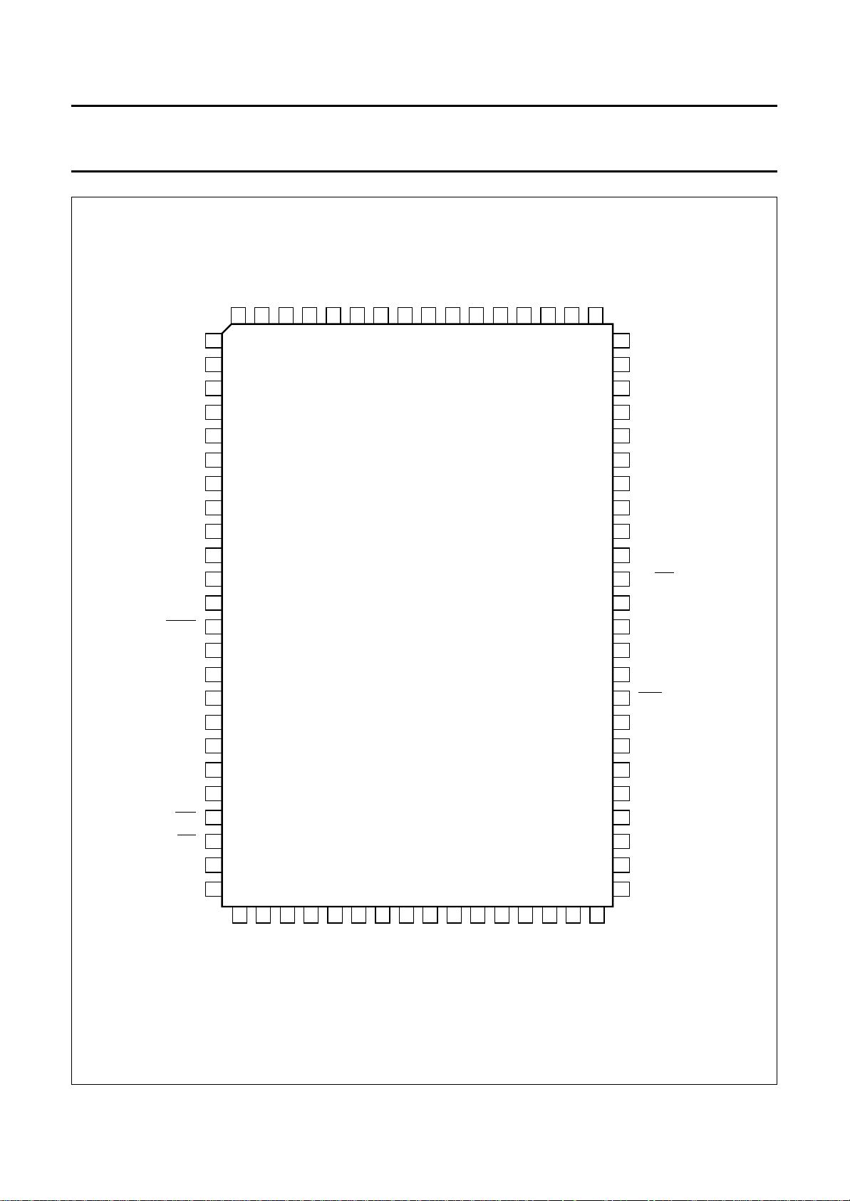
Fig.3 Pin configuration (SOT318-2; QFP80).
A1
36
37
38
39
40
MGB380
A2
A3
A4
SS3
V
Page 8
Philips Semiconductors Preliminary specification
Drive processor for DCC systems SAA2023
FUNCTIONAL DESCRIPTION
MBD620
RAM
41464
DRIVE
CAPSTAN
speed control
64K x 4
BUFFER
WRAMP
2
I S
sub-band
TDA1381
WRITE AMP.
DRP
SAA2023ORSAA3323
TAPE
HEAD
FIXED
RDAMP
TDA1380
DRIVE
PROCESSOR
READ AMP.
DRIVERS
MECHANICS
search data
detect
switch
SYSTEM
MICROCONTROLLER
TAPE DRIVE PROCESSING
SYSTEM CONTROL
handbook, full pagewidth
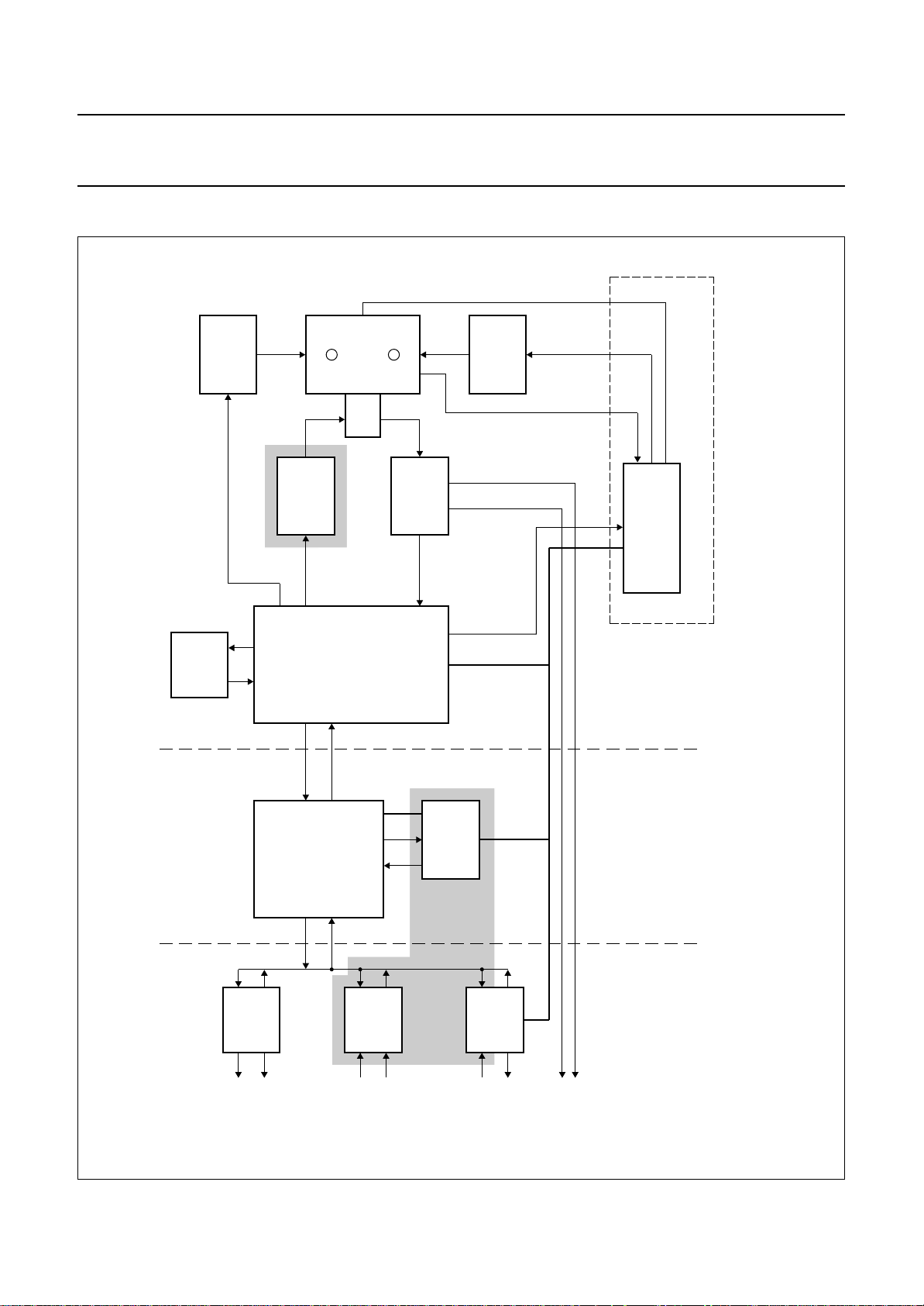
Fig.4 DCC system block diagram.
May 1994 8
L
DAC
TDA1305
output
analog
R
SFC3
SAA2003
baseband
STEREO
2
I S
L
ADC
SAA7366
input
analog
2
R
FILTER CODEC
ADAS3
filtered I S
SAA2013
ADAPTIVE
ALLOCATION
DIGITAL
TDA1315
AUDIO I/O
IEC958
L output
analog CC
analog CC
AUDIO IN/OUT PASC PROCESSOR
R output
Page 9
Philips Semiconductors Preliminary specification
Drive processor for DCC systems SAA2023
A simplified block diagram of the SAA2023 is shown in
Fig.1.
DCC drive processing
The SAA2023 provides the following functions for the DCC
drive processing.
LAYBACK MODES
P
• Analog-to-digital conversion
• Tape channel equalization
• Tape channel data and clock recovery
• 10-to-8 demodulation
• Data placement in system RAM
• C1 and C2 error correction decoding
• Interfacing to sub-band serial PASC interface
• Interfacing to microcontroller for SYSINFO and AUX
data
• Capstan control for tape deck.
R
ECORD MODES
• Interfacing to sub-band serial PASC interface
• C1 and C2 error correction encoding
• Formatting for tape transfer
• 8-to-10 modulation
• Interfacing to microcontroller for SYSINFO and AUX
data
• Capstan control for tape deck, programmable by
microcontroller.
EARCH MODE
S
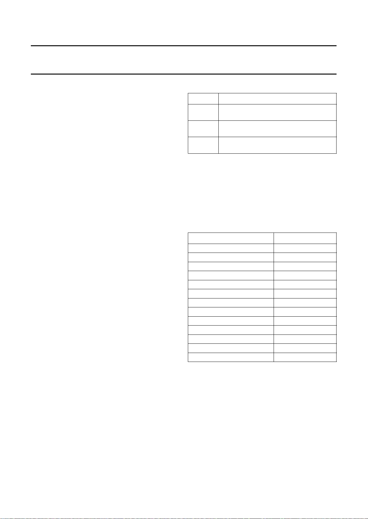
Table 1 Basic modes of TFE module.
MODE EXPLANATION
DPAP audio and SYSINFO (main data) play;
AUX play
DPAR audio and SYSINFO (main data) play;
AUX record
DRAR audio and SYSINFO (main data) record;
AUX record
REGISTERS
TFE
The TFE module has 8 writable and 5 readable registers
that are accessible via the L3 interface, one write register
(CMD) and four read registers (STATUS0 to STATUS3)
which are directly addressable, the other registers are
indirectly addressable via commands sent to the CMD
register. The registers are named as shown in Table 2.
Table 2 TFE register names.
REGISTER NAME READ/WRITE
CMD W
STATUS0 R
STATUS1 R
STATUS2 R
STATUS3 R
SET0 W
SET1 W
SET2 W
SET3
(1)
W
SPDDTY W
BYTCNT W
RACCNT W
SPEED R
• Detection and interpretation of AUX envelope
information
• AUX envelope counting
• Search speed estimation.
Tape Formatting and Error (TFE) correction module
The TFE module has 3 basic modes of operation as shown
in Table 1.
May 1994 9
Note
1. The 4 LSBs of register ‘SET3’ set RAM type (RType)
and RAM timing (RTim). See Table 3.
For normal operation the 4 MSBs of register ‘SET3’
should be logic 0.
Page 10
Philips Semiconductors Preliminary specification
Drive processor for DCC systems SAA2023
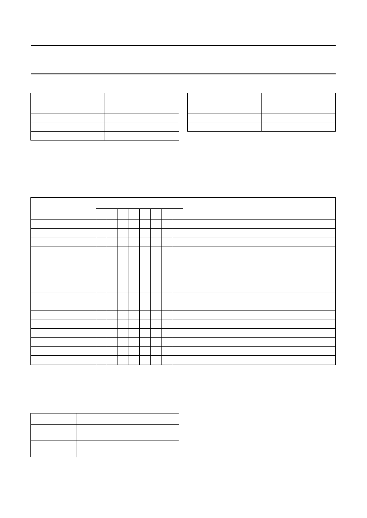
Table 3 RAM settings by register SET3.
RAM REGISTER SET3
RTYPE 0 bit 0
RTYPE 1 bit 1
RTim 0 bit 2
RTim 1 bit 3
TFE
DATA STREAMS
The TFE module has three read/write data streams that
are accessible via the L3 interface and they are shown in
Table 4.
Table 5 TFE commands.
NAME
RDSPEED 00000000read SPEED register
LDSET0 00010000load new TFE settings register 0
LDSET1 00010001load new TFE settings register 1
LDSET2 00010010load new TFE settings register 2
LDSET3 00010011load new TFE settings register 3
LDSPDDTY 00010101load SPDDTY register
LDBYTCNT 00010111load BYTCNT register
LDRACCNT 00011000load RACCNT register
RDAUX 00100000read AUXILIARY information
RDSYS 00100001read SYSINFO
RDDRAC Y Z 100010read RAM data bytes (8 bits) from quarter YZ
RDWDRAC Y Z 100011read RAM data words (12 bits) from quarter YZ
WRAUX 00110000write AUXILIARY information
WRSYS 00110001write SYSINFO
WRDRAC Y Z 110010write RAM data bytes (8 bits) to quarter YZ
WRWDRAC Y Z 110011write RAM data words (12 bits) to quarter YZ
COMMAND BYTE
76543210
Table 4 TFE data streams.
DATA STREAM NAME READ/WRITE
SYSINFO R/W
AUXINFO R/W
Scratch pad RAM R/W
COMMANDS’
TFE ‘
These are the commands that need to be sent to the TFE
in order to access the indirectly accessible registers and
the data streams, see Table 5.
EXPLANATION
Digital equalizer module
The digital equalizer module has 2 basic modes of
operation as shown in Table 6.
Table 6 Basic modes of equalizer module.
MODE EXPLANATION
Play main data and AUX channels are
equalized
Search only AUX channel is processed; AUX
envelope information is processed
May 1994 10
DIGITAL EQUALIZER REGISTERS
The digital equalizer module has 9 write only, 3 read only
and 1 read/write register(s) that are accessible via the
L3 interface, one write register (CMD) and 2 read registers
(STATUS0 and STATUS1) which are directly addressable,
the other registers are indirectly addressable via
commands sent to the CMD register. The registers are
named as shown in Table 7.
Page 11
Philips Semiconductors Preliminary specification
Drive processor for DCC systems SAA2023
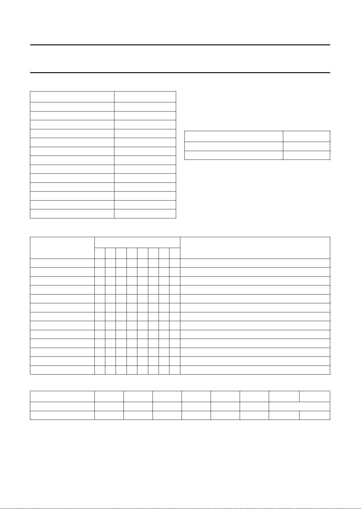
Table 7 Digital equalizer register names.
REGISTER NAME READ/WRITE
CMD W
STATUS0 R
STATUS1 R
COEFCNT W
FCTRL W
CHT1SEL W
CHT2SEL W
ANAEYE W
AEC R/W
SSPD R
INTMASK W
DEQ2SET W
CLKSET W
Table 9 Digital equalizer commands.
COMMAND BYTE
NAME
76543210
WRCOEF 00110000write FIR coefficients to the digital equalizer buffer bank
RDCOEF 00100000read FIR coefficients from the digital equalizer active bank
LDCOEFCNT 00010011load FIR coefficient counter
LDFCTRL 00010100load filter control register
LDT1SEL 00010110load CHTST1 pin selection register
LDT2SEL 00010111load CHTST2 pin selection register
LDTAEYE 00011000load ANAEYE channel selection register
LDAEC 00011001load AEC counter
RDAEC 00100010read AEC counter
RDSSPD 00100100read SEARCH speed register
LDINTMSK 00010010load interrupt mask register
LDDEQ3SET 00010000load digital equalizer settings register
LDCLKSET 00010001load PLL clock extraction settings register
DATA STREAMS
The digital equalizer module has one write only and one
read only data stream that are accessible via the
L3 interface and they are shown in Table 8.
Table 8 Digital equalizer data streams.
DATA STREAM NAME READ/WRITE
FIR coefficients to buffer bank W
FIR coefficients from active bank W
IGITAL EQUALIZER “COMMANDS”
D
These are the commands that need to be sent to the digital
equalizer in order to access the indirectly accessible
registers and the data streams.
EXPLANATION
Table 10 Filter control register.
BIT 7654321 0
Meaning −−−µCS
Default 0 0 0 0 1 0 1 1
Note
1. µCS is a microcontroller controlled coefficient bank switch. This causes the filter coefficients to be activated at a time
that is safe for the digital equalizer, i.e. at the end of the FIR program and that the complete value of coefficient
number 9 has been received.
May 1994 11
(1)
SH1 SH0 Reserved
Page 12
Philips Semiconductors Preliminary specification
Drive processor for DCC systems SAA2023
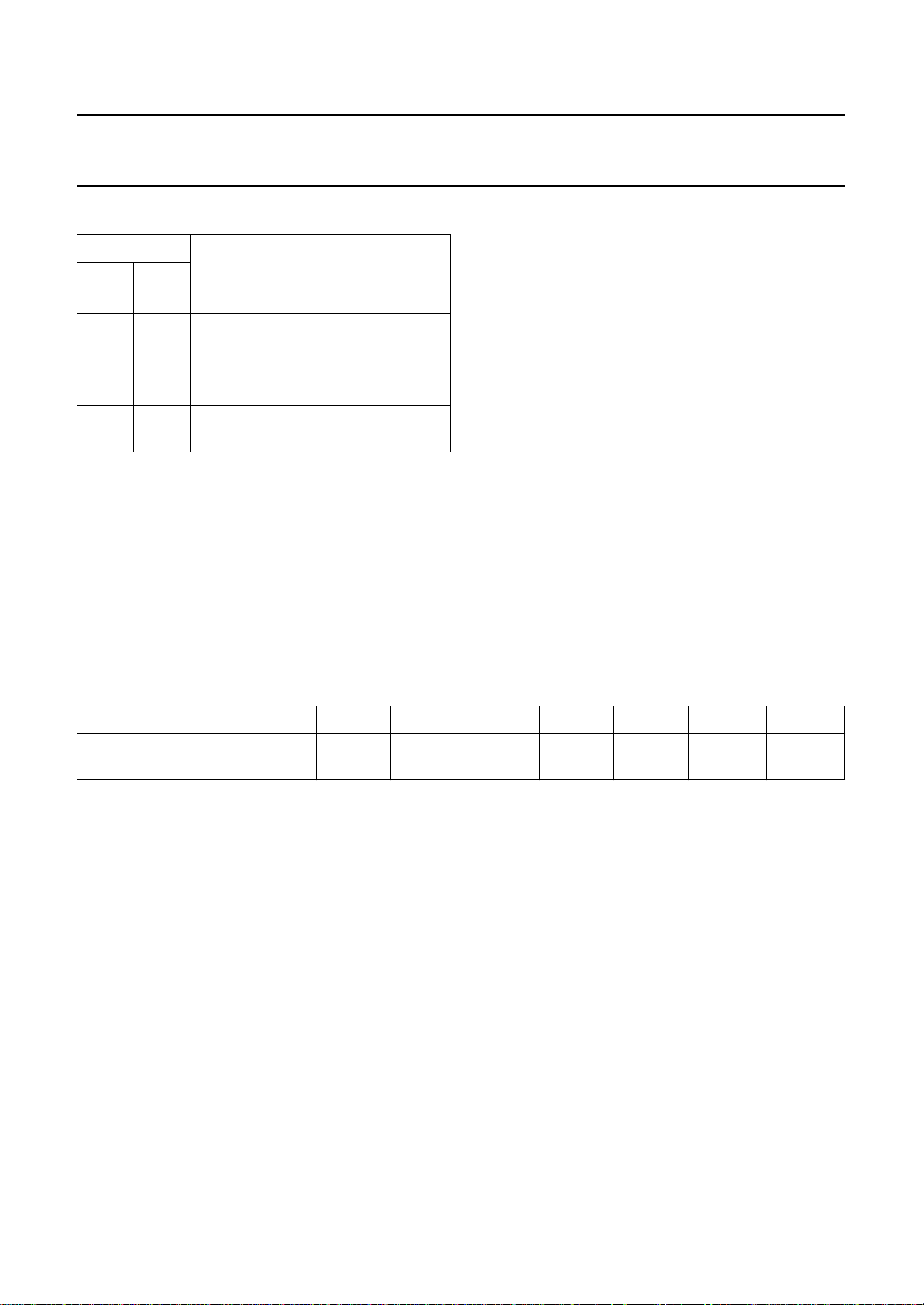
Table 11 SH1 and SH2 (FIR output scaling).
SH
10
0 0 FIR mod 256
01
10
11
EFFECT ON FIR OUTPUT
FIR
mod 256
---------2
FIR
mod 256
---------4
FIR
mod 256
---------8
Transfer of FIR coefficients
For the main data channels (tracks 0 to 7) there are
10 coefficients (taps) each of 8 bits, where all of the data
channels make use of the same coefficients. The
addresses for the main data coefficients 0 to 9 are
0to9
There are ten coefficients (taps) each of 8 bits for the aux
channel (CHAUX). The addresses for the auxiliary
coefficients 0 to 9 are 16 to 25
respectively.
dec
respectively.
dec
There are 2 banks of coefficients for both the aux and the
main data channels, namely the ‘buffer’, and the ‘active’
banks. The microcontroller writes only to the ‘buffer’
banks, and reads only from the ‘active’ banks.
The microcontroller can poll the digital equalizer status bit
BKSW to see when the switch occurs. BKSW starts life
LOW, goes HIGH as a result of the bank switching and
goes LOW as result of the complete value of a main data
coefficient being received by the digital equalizer.
The microcontroller sets µCS HIGH before sending the
new set of aux or main data coefficients, the digital
equalizer resets it once the bank switch occurs.
The actual FIR coefficients that are used are a function of
the tape head, read amplifier and type of tape (i.e.
pre-recorded or own recorded) used, such information is
outside of the scope of this data sheet.
Coefficient address counter (COEFCNT)
This 5 bit counter is used to point to the FIR coefficient to
be transferred to or from the digital equalizer.
Table 12 Coefficient address counter.
BIT 7654321 0
Meaning −−−CC4 CC3 CC2 CC1 CC0
Default 0 0 0 0 0 0 0 0
Pin explanations and interfacing to other hardware
RESET
This is an active HIGH input which resets the SAA2023
and brings it into its default mode, DPAP. This reset does
not affect the contents of the FIR filter coefficients in the
digital equalizer. This should be connected to the system
reset, which can be driven by the microcontroller. The
duration of the reset pulse should be at least 15 µs.
SLEEP
This pin is an active HIGH input which puts the SAA2023
in a low power consumption SLEEP mode. This pin should
be connected to the DCC SLEEP signal, which can be
driven by the microcontroller. The CLK24 clock may be
stopped and the VREFP and VREFN inputs brought to
ground while the SAA2023 is in ‘sleep’ mode to further
reduce power consumption. When recovering from sleep
mode, the SLEEP pin should be taken LOW and the
SAA2023 reset.
CLK24
This is the 24.576 MHz clock input and should be
connected directly to the SAA2003 (pin CLK24).
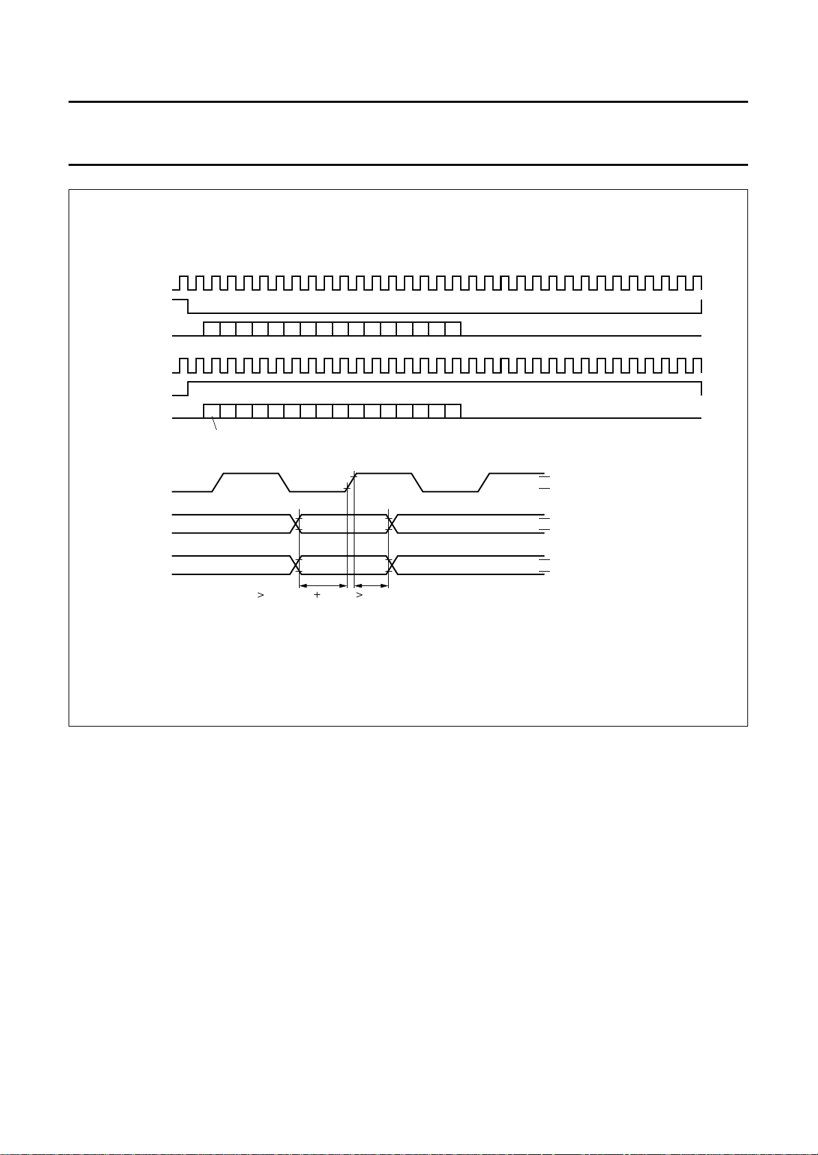
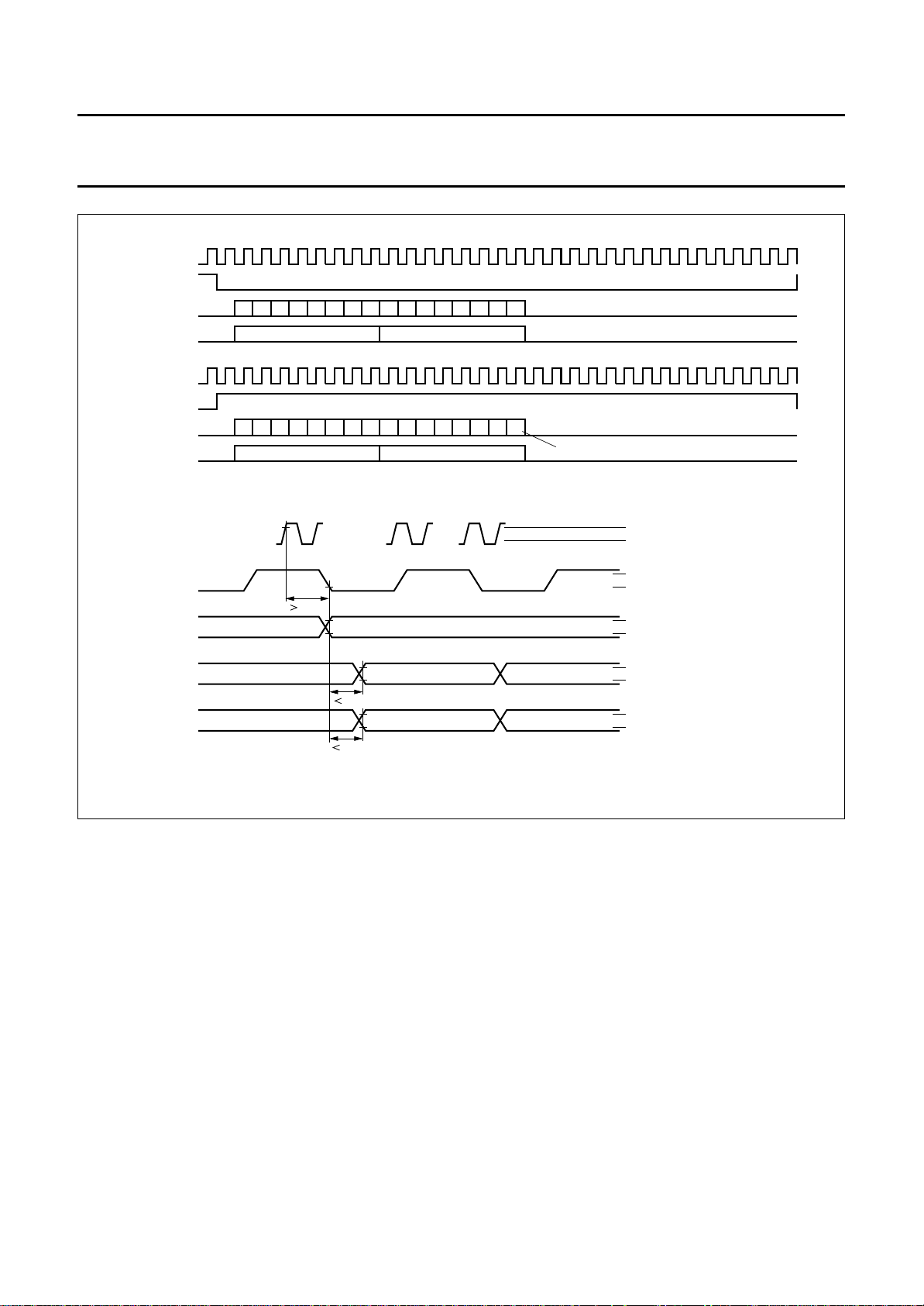
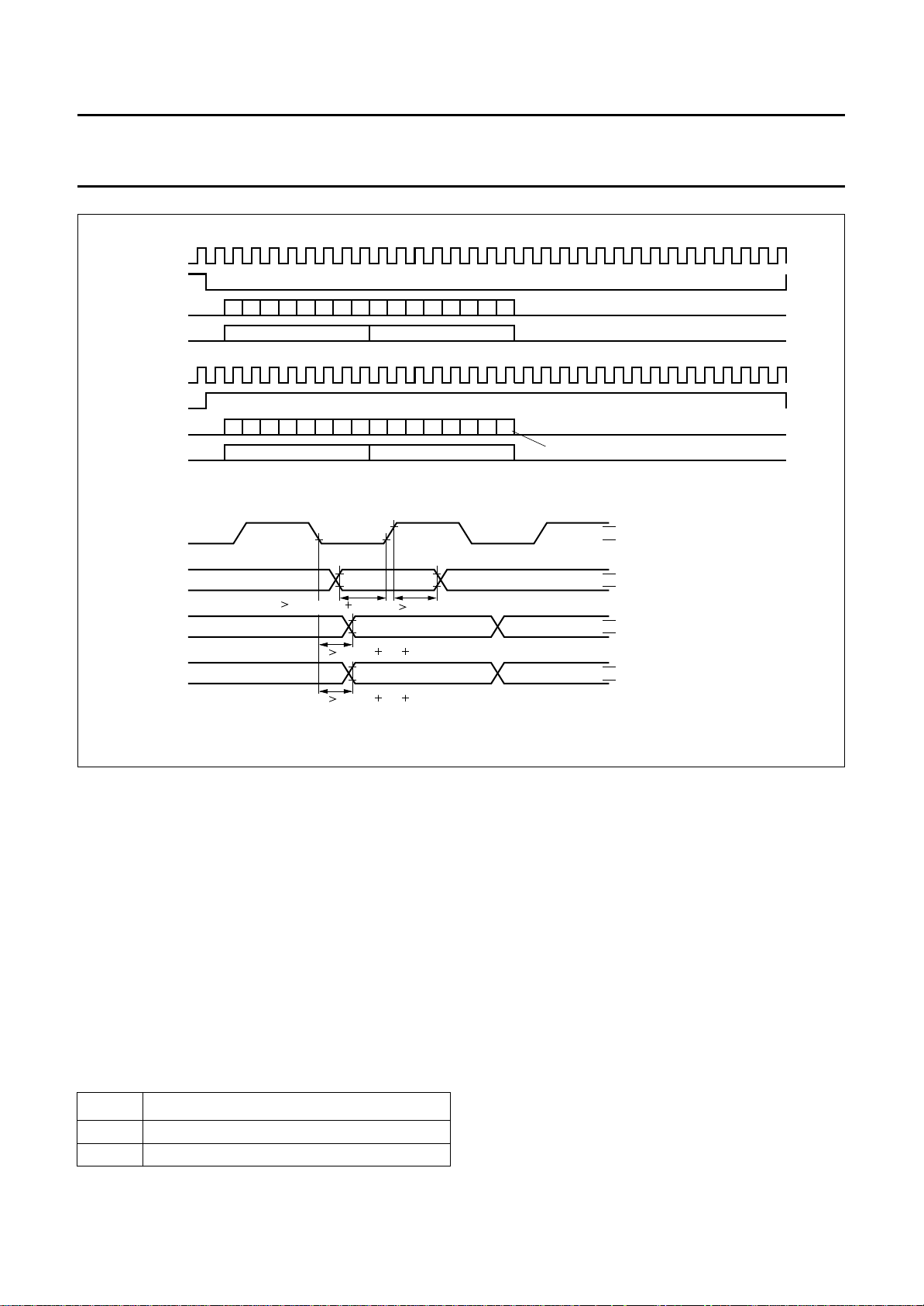
Sub-band serial PASC interface connections
The timing for the sub-band serial PASC interface is given
in Figs 5 to 7.
May 1994 12
Page 13
Philips Semiconductors Preliminary specification
Drive processor for DCC systems SAA2023
handbook, full pagewidth
SBCL(in)
SBWS(in)
SBDA(in)
SBCL(in)
SBWS(in)
SBDA(in)
SBCL(in)
SBWS(in)
SBDA(in)
bit number
2 x t 40 ns
MCLK
40 ns
1514131211109876543210
31302928272625242322212019181716
V
IH
V
OH
V
IH
V
OH
V
IH
V
OH
MGB381
Fig.5 Sub-band serial PASC interface timing; DRAR mode.
May 1994 13
Page 14
Philips Semiconductors Preliminary specification
Drive processor for DCC systems SAA2023
handbook, full pagewidth
SBCL(out)
SBWS(out)
SBDA(out)
SBEF(out)
SBCL(out)
SBWS(out)
SBDA(out)
SBEF(out)
SBMCLK(in)
SBCL(out)
SBWS(out)
SBDA(out)
SBDA(out)
60 ns
7 ns
7 ns
1514131211109876543210
31302928272625242322212019181716
bit number
V
IH
V
IL
V
OH
V
OL
V
OH
V
OL
V
OH
V
OL
V
OH
V
OL
MGB382
Fig.6 Sub-band serial PASC interface timing in play modes; DRPMAS = logic 1.
May 1994 14
Page 15
Philips Semiconductors Preliminary specification
Drive processor for DCC systems SAA2023
handbook, full pagewidth
SBCL(in)
SBWS(in)
SBDA(out)
SBEF(out)
SBCL(in)
SBWS(in)
SBDA(out)
SBEF(out)
SBCL(in)
SBWS(in)
SBDA(out)
SBDA(out)
2 x t 40 ns
MCLK
t (40 85) ns
MCLK
t (40 40) ns
MCLK
40 ns
1514131211109876543210
31302928272625242322212019181716
bit number
V
IH
V
IL
V
IH
V
IL
V
OH
V
OL
V
OH
V
OL
MGB383
Fig.7 Sub-band serial PASC interface timing in play modes; DRPMAS = logic 0.
SBMCLK
This is the sub-band master clock input for the sub-band
serial PASC interface. The frequency of this signal is
nominally 6.144 MHz. When the SAA2023 is used with
SAA2003 this pin is tied to ground, and the TFE settings
bit ‘DRPMAS’ set to logic 1.
SBDIR
This output pin is the sub-band serial PASC bus direction
signal, it indicates the direction of transfer on the sub-band
serial PASC bus. This pin connects directly to the SBDIR
pin on the SAA2003. The transfer directions are shown in
Table 13.
Table 13 PASC bus transfer directions.
SBDIR DIRECTION
1 SAA2023 to SAA2003 transfer (audio play)
0 SAA2003 to SAA2023 transfer (audio record)
SBCL
This input/output pin is the bit clock line for the sub-band
serial PASC interface to the SAA2003. When used with
SAA2003 this pin is input only. It has a nominal frequency
of 768 kHz.
SBWS
This input/output pin is the word select line for the
sub-band serial PASC interface to the SAA2003. When
used with SAA2003 this pin is input only. It has a nominal
frequency of 12 kHz.
SBDA
This input/output pin is the serial data line for the sub-band
serial PASC interface to the SAA2003.
SBEF
This active HIGH output pin is the error-per-byte line for
the sub-band serial PASC interface to the SAA2003.
May 1994 15
Page 16
Philips Semiconductors Preliminary specification
Drive processor for DCC systems SAA2023
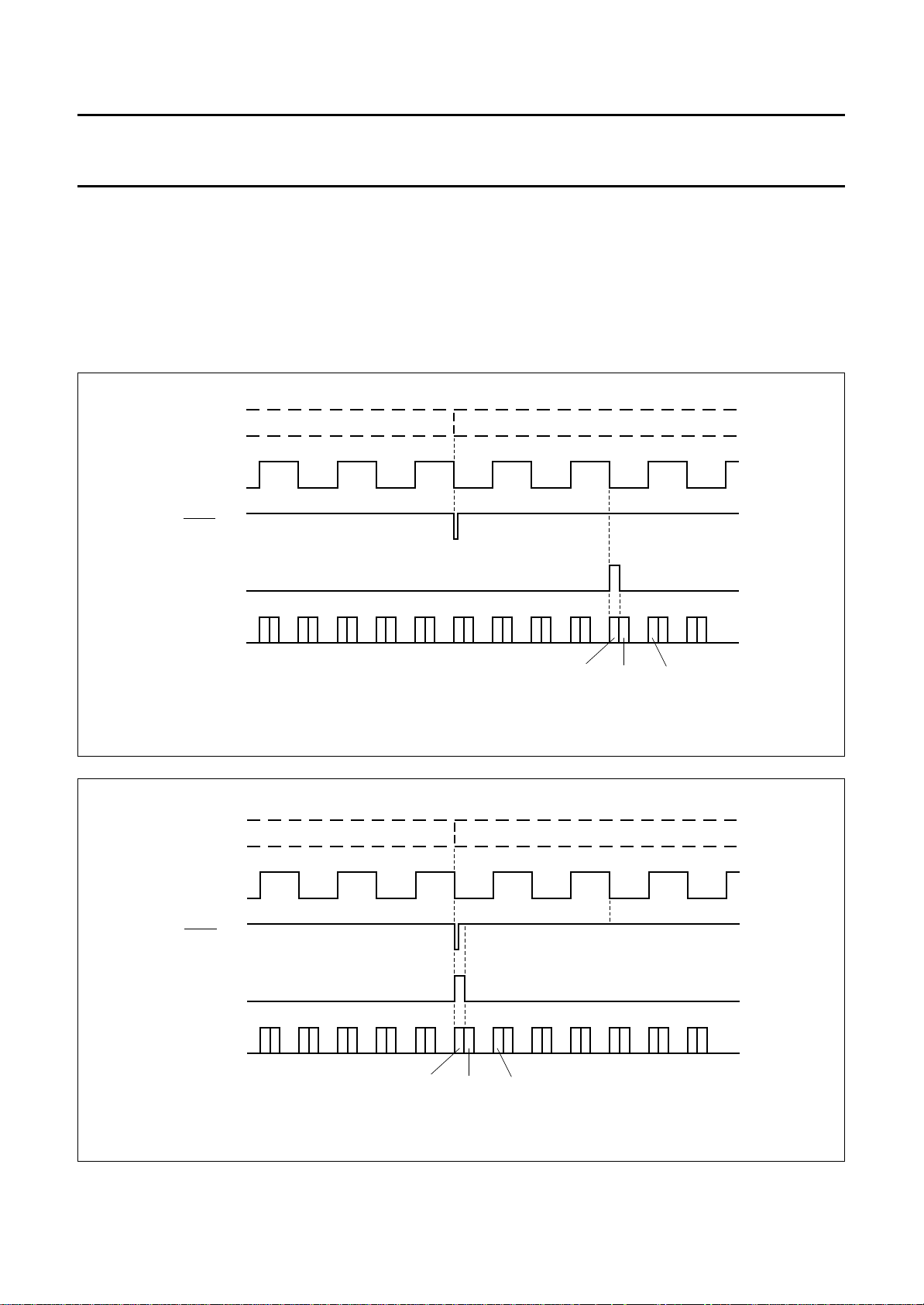
URDA
This active HIGH output pin indicates that the main data
(audio), the SYSINFO and the AUXILIARY data are NOT
usable, regardless of the state of the corresponding
reliability flags. The state of this pin is reflected in the
URDA bit of STATUS byte 0, which can be read by the
microcontroller. This pin should be connected directly to
handbook, full pagewidth
SNUM
SBWS
L3REF
'FIRST BYTE"
SBDA
0
the URDA pin of the SAA2003. URDA goes active as a
result of a reset, a mode change from mode DRAR to
DPAP, or if the SAA2023 has had to re-synchronize with
the incoming data from tape.
The position of the first sub-band serial PASC bytes in a
tape frame is shown in Figs 8 and 9.
1
MGB384
byte 0
byte 1 byte 2
Fig.8 Position of first sub-band serial PASC bytes in a tape frame in DPAP/DPAR mode.
handbook, full pagewidth
SNUM
SBWS
L3REF
'FIRST BYTE'
SBDA
30
byte 0 byte 1 byte 2
Fig.9 Position of first sub-band serial PASC bytes in a tape frame in DRAR mode.
MGB385
May 1994 16
Page 17
Philips Semiconductors Preliminary specification
Drive processor for DCC systems SAA2023
RAM connections
The SAA2023 has been designed to operate with DRAMs
and SRAMs. Suitable DRAMs are 64K × 4-bit or
256K × 4-bit configurations operating in page mode, with
an access time of 80 to 100 ns. The timing for read, write
and refresh cycles for DRAMs is shown in Figs 10 to 12.
The timing for SRAMs is shown in Figs 13 to 19.
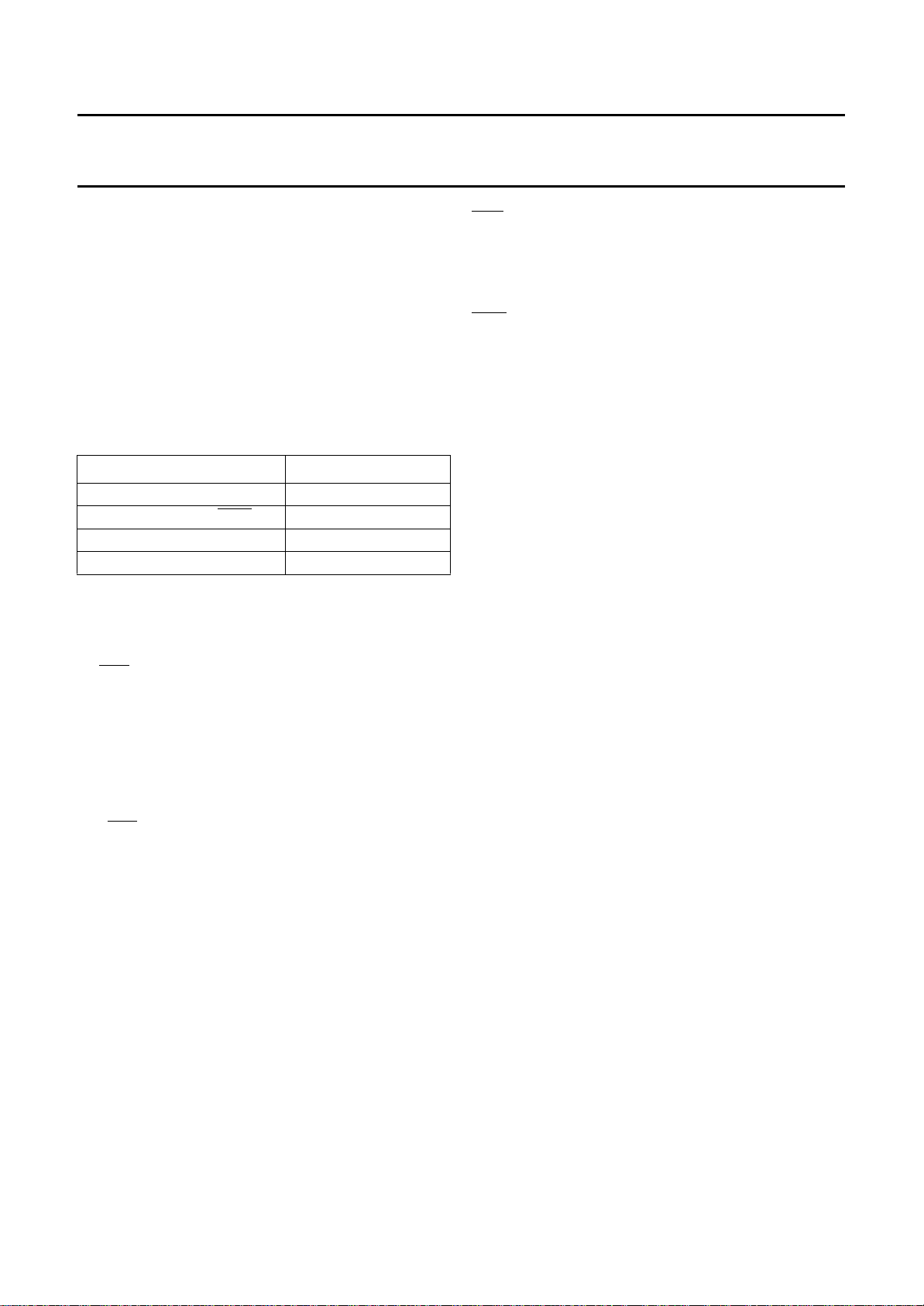
For fast SRAMs: (these values are subject to verification
during characterization). The conditions (most critical at
the required VDD) are shown in Table 14.
Table 14 Fast SRAM conditions.
CONDITION
Write pulse duration t
Data set-up to rising
Write cycle time T
Read access time t
(1)
≤ 140 ns
W
WEN tsu≤ 72 ns
≤ 200 ns
cy
≤ 240 ns
ACC
TIME
Note
1. The SAA2023 should work in: RType = ‘01’;
RTim = ‘00’ mode.
CAS
A9/
When SAA2023 is used with SRAM this output pin is
Address line 9, and should be connected directly to the
corresponding address pin on the SRAM. When SAA2023
is used with DRAM this output pin is the column address
strobe (active LOW), it connects directly to the column
address strobe pin of the DRAM.
RAS
A10/
When SAA2023 is used with SRAM this output pin is
Address line 10, and should be connected to the
corresponding address pin of the SRAM. When SAA2023
is used with DRAM this output pin is the row address
strobe (active LOW), it connects directly to the row
address strobe pin of the DRAM.
OEN
This output pin is the output enable (active LOW) for the
RAM, it connects directly to the output enable pin of the
RAM.
WEN
This output pin is the write enable (active LOW) for the
RAM, it connects directly to the write enable pin of the
RAM.
TO A8
A0
When SAA2023 is used with DRAM these output pins are
the multiplexed column and row address lines. When the
64K × 4-bit DRAM is used, pins A0 to A7 should be
connected to the DRAM address input pins, and pin A8
should be left unconnected. When using the 256K × 4-bit
DRAM the address pins A0 to A8 should be connected to
the address input pins of the DRAM.
When SAA2023 is used with SRAM these are the lower
address pins and should be connected directly to the
SRAM address pins.
A11
This output pin is the an address pin for the SRAM and
when SRAM is used they should be connected directly to
the address pins of the SRAM. When DRAM is used this
pin should not be connected.
AND A12 TO A16
A10
These output pins are the upper address pins for the
SRAM and when SRAM is used they should be connected
directly to the address pins of the SRAM. When DRAM is
used or when the small SRAM is used all or some of these
pins become available as Port expander outputs.
May 1994 17
Page 18
Philips Semiconductors Preliminary specification
Drive processor for DCC systems SAA2023
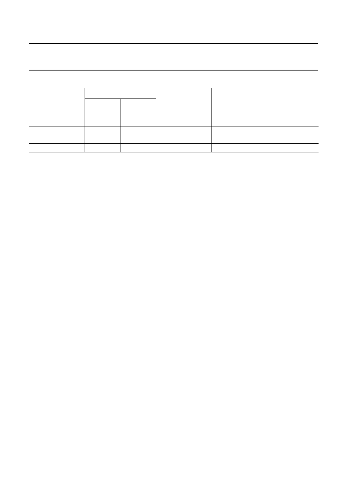
Table 15 Port expander outputs.
PIN NAME
A14/PINO1 46 44 PINO1 RType = 00
A13/PINO2 50 48 PINO2 RType = 00
A16/PINO3 47 45 PINO3 RType = 00 or RType = 01
A15/PINO4 48 46 PINO4 RType = 00 or RType = 01
A12/PINO5 45 43 PINO5 RType = 00
TO D3
D0
When SAA2023 is used with SRAM these I/O pins form the lower nibble of the data bus connection to the RAM, and
should be connected to the corresponding data I/O pins of the SRAM. When SAA2023 is used with DRAM these
input/output pins are the data lines for the RAM, they should be connected directly to the DRAM data I/O pins.
D4
TO D7
These input/output pins are the upper nibble of the data bus for use with SRAM, and when SRAM is being used they
should be connected directly to the corresponding SRAM I/O pins.
QFP80 TQFP80
PIN
PORT EXPANDER
OUTPUT
CONDITIONS
May 1994 18
Fig.10 DRAM read cycle timing.
 Loading...