

Page 1

INTEGRATED CIRCUITS
DATA SH EET
SAA2002
Stereo filter and codec
Product specification
Supersedes data of February 1993
File under Integrated Circuits, Miscellaneous
Philips Semiconductors
December 1993
Page 2

Philips Semiconductors Product specification
Stereo filter and codec SAA2002
FEATURES
• Stereo filtering and codec functions in a single chip
• Drive processing interface
• Filtered data interface
• Baseband audio data interface
• LT interface to microcontroller
• Clock generator
• Low operating voltage capability.
GENERAL DESCRIPTION
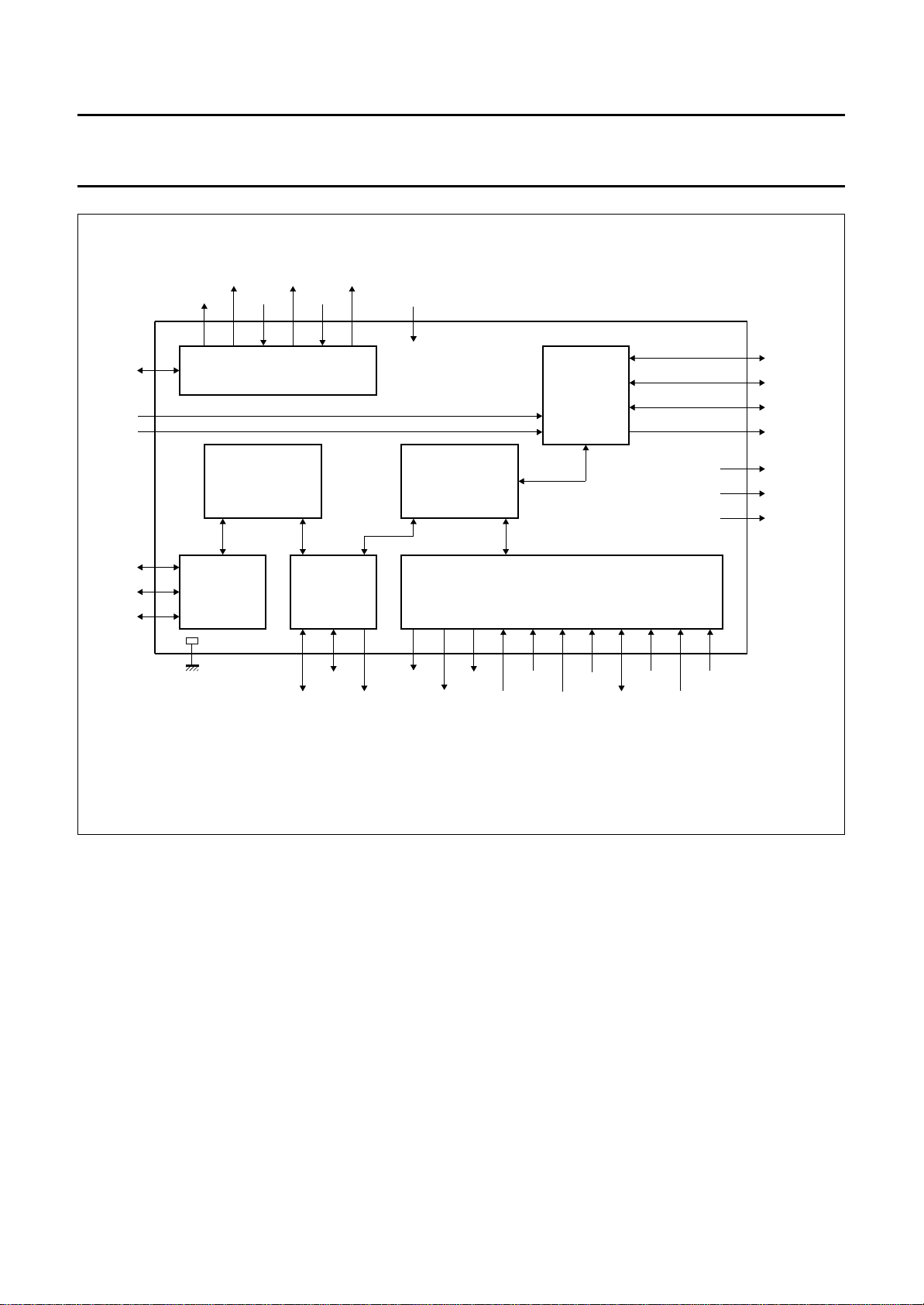
The SAA2002 performs the sub-band filtering and audio
frame codec functions in a Precision Adaptive Sub-band
Coding (PASC) system. It is capable of functioning as a
stand-alone decoder, but requires the addition of an
Adaptive Allocation and Scale factor processor (SAA2012)
in order to perform PASC encoding in a DCC
record system.
ORDERING INFORMATION
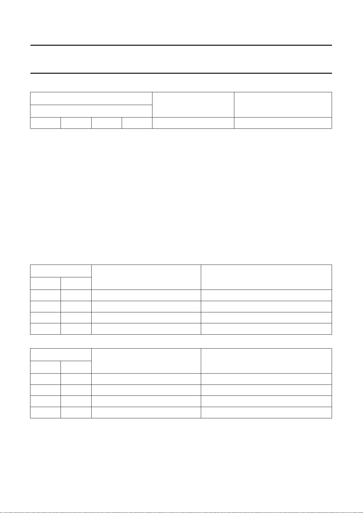
EXTENDED TYPE
NUMBER
SAA2002GP 44 QFP
Note
1. When using reflow soldering it is recommended that the Dry Packing instructions in the Quality Reference
Pocketbook are followed. The pocketbook can be ordered using the code 9398 510 34011.
PINS PIN POSITION MATERIAL CODE
(1)
PACKAGE
plastic SOT205AG
December 1993 2
Page 3
Philips Semiconductors Product specification
Stereo filter and codec SAA2002
FS256
SBDIR
SBEF
SWS
SCL
SDA
CLK24 X22OUT X24OUT
CLK22 X22IN X24IN
38 39 40 41 42 43 28,44
1
7
11
20
19
21
CLOCK GENERATOR
SUB-BAND
PROCESSOR
BASEBAND
SERIAL
INTERFACE
5,37
V
SS
STEREO
FILTER
FILTERED
DATA
INTERFACE
FDAF
FDAC FSYNC
V
DD
15
FRESET
SAA2002
PASC
CODEC
PROCESSOR
14 13 36 35 34 33 32 22 29 618 17 16
SYNCDAI
FDIR
SUB-BAND
SERIAL
INTERFACE
MICROPROCESSOR
INTERFACE & CONTROL
LTCLK
LTCNT1 LTENSFC
PWRDWN
LTDATA
RESET
8
SBDA
9
SBCL
10
SBWS
12
SBMCLK
2
MUTEDAC
3
DEEMDAC
4
ATTDAC
MEA655 - 1
URDALTCNT0
Fig.1 Block diagram.
December 1993 3
Page 4

Philips Semiconductors Product specification
Stereo filter and codec SAA2002
PINNING
SYMBOL PIN DESCRIPTION
FS256 1 filtered-I2S clock; 256 x fs; 12 mA, 3-state output + CMOS input with pull-down
MUTEDAC 2 DAC control/output expander
DEEMDAC 3 DAC control/output expander
ATTDAC 4 DAC control/output expander
V
SS
URDA 6 unreliable drive processing data; CMOS level
SBDIR 7 sub-band I
SBDA 8 sub-band I
SBCL 9 sub-band I
SBWS 10 sub-band I
SBEF 11 sub-band I
SBMCLK 12 sub-band I
SYNCDAI 13 Digital Audio Interface (DAI) synchronization pulse
FDIR 14 filtered-I
FRESET 15 reset signal for SAA2012
FSYNC 16 filtered-I
FDAF 17 filtered-I
FDAC 18 filtered-I
SCL 19 I
SWS 20 I
SDA 21 I
PWRDWN 22 sleep mode; CMOS level
DSC4 23 test pin; not to be connected
DSC3 24 test pin; not to be connected
DSC2 25 test pin; not to be connected
DSC1 26 test pin; not to be connected
DSC0 27 test pin; not to be connected
V
DD
RESET 29 system reset input; CMOS level with pull-down and hysteresis
T1 30 test pin; not to be connected
T0 31 test pin; not to be connected
LTDATA 32 LT interface data; 4 mA, 3-state output + CMOS input with pull-down
LTCLK 33 LT interface bit clock input; CMOS level
LTENSFC 34 LT interface enable input; CMOS level
LTCNT0 35 LT interface control input; CMOS level
LTCNT1 36 LT interface control input; CMOS level
V
SS
CLK22 38 22.5792 MHz buffered output
CLK24 39 24.576 MHz buffered output
5 supply ground (0 V)
2
S direction: (SWBS, SBCL, SBDA); CMOS level
2
S data; 4 mA, 3-state output + CMOS input with pull-down
2
S bit-clock; 4 mA, 3-state output + CMOS input with pull-down
2
S word select; 4 mA, 3-state output + CMOS input with pull-down
2
S byte error flag input; CMOS level
2
S clock; 6.144 MHz locked to FS256; 8 mA, 3-state output + CMOS input
with pull-down
2
S direction: (FDAC, FDAF and SDA)
2
S synchronization signal for SAA2012
2
S sub-band filter data; 4 mA, 3-state output + CMOS input with pull-down
2
S sub-band codec data; 4 mA, 3-state output + CMOS input with pull-down
2
S bit-clock; 4 mA, 3-state output + CMOS input with pull-down
2
S word select; 4 mA, 3-state output + CMOS input with pull-down
2
S baseband data filter; 4 mA, 3-state output + CMOS input with pull-down
28 supply voltage (+5 V)
37 supply ground (0 V)
December 1993 4
Page 5

Philips Semiconductors Product specification
Stereo filter and codec SAA2002
SYMBOL PIN DESCRIPTION
X22IN 40 22.5792 MHz crystal input
X22OUT 41 22.5792 MHz crystal output
X24IN 42 24.576 MHz crystal input
X24OUT 43 24.576 MHz crystal output
V
DD
44 supply voltage (+5 V)
FS256
MUTEDAC
DEEMDAC
ATTDAC
V
SS
URDA
SBDIR
SBDA
SBCL
SBWS
SBEF
FDAF
V
CLK22
38
18
FDAC
SS
37
19
SCL
LTCNT0
LTCNT1
36
35
21
20
SDA
SWS
LTENSFCPWRDWN
34
33
32
31
30
29
28
27
26
25
24
23
22
LTCLK
LTDATA
T0
T1
RESET
V
DD
DSC0
DSC1
DSC2
DSC3
DSC4
MEA640 - 1
DD
X24IN
42
14
FDIR
X22IN
X22OUT
41
40
SAA2002
15
16
FSYNC
FRESET
CLK24
39
17
V
X24OUT
44
43
1
2
3
4
5
6
7
8
9
10
11
12
13
SBMCLK
SYNCDAI
December 1993 5
Fig.2 Pin configuration.
Page 6

Philips Semiconductors Product specification
Stereo filter and codec SAA2002
and
drive
capstan
heads
tape
write
TDA1319
TDA1316 or
speed control
2
codec
SAA2002
stereo filter
I S
(sub-band)
read
SAA2032
SAA2022
adaptive
SAA2012
TDA1318
TDA1317 or
digital
equalizer
RAM
scale factors
allocation and
TAPE DRIVE PROCESSING
256 kbits
MEA695 - 2
MICROCONTROLLER
Fig.3 DCC data flow diagram.
December 1993 6
2
I S
ADC
SAA7360
RECORDING + PLAY BACK
input
analog
DAC
SAA7323
output
analog
DAIO
TDA1315
digital input
digital output
AUDIO INPUT/OUTPUT PASC PROCESSING
Page 7

Philips Semiconductors Product specification
Stereo filter and codec SAA2002
FUNCTIONAL DESCRIPTION
PASC
Precision Adaptive Sub-band Coding achieves highly
efficient digital encoding of audio signals by using an
algorithm based on the characteristics of the human
auditory system.
The broad-band audio signal is split into 32 sub-band
signals during encoding. For each of the sub-band signals
the masking threshold is calculated. The samples of the
sub-bands are incorporated in the PASC signal with an
accuracy that is determined by the signal to masking
threshold ratio for that sub-band.
During decoding, the sub-band signals are reconstructed
and combined into a broadband audio signal. The
integrated filter processor performs the splitting (encoding)
and joining (decoding) including the corresponding
formatting functions.
For encoding, a SAA2012 is necessary to calculate the
masking threshold and required accuracy of the
sub-band samples.
Encoding (see Fig.4)
An encoding algorithm table is used during the recording
process but, due to the Adaptive Allocation functions of the
SAA2012, this may change with every frame. The table is
therefore calculated for each frame by the SAA2012 and
then transferred to the SAA2002.
A frame contains 2 x 384 samples of Left and Right audio
data. This results in 12 samples per sub-band
(32 sub-bands). The samples of the greatest amplitude
are used to determine the scale factor for a given
sub-band. All samples are then scaled to represent a
fraction of the greatest amplitude.
Once scaled, the samples are quantified to reduce the
number of bits to correspond with the allocation table as
calculated by the SAA2012. Synchronization and coding
information data is then added to result in a fully encoded
PASC signal.
This is followed by a process of multiplication to provide
de-quantification and de-scaling of the PASC samples.
The decoded sub-band samples, which are represented in
24-bit two’s complement notation, are processed by the
sub-band filters and reconstituted into a single digital
audio signal.
RESET
Reset must be active from system power-up, or the end of
sleep mode (falling edge of PWRDWN), for a period
equivalent to 24 cycles of CLK24 plus the crystal oscillator
start-up time.
Sleep mode
A HIGH input applied to the PWRDWN pin will halt all
internally generated clock signals. As a result, chip activity
will halt completely with outputs frozen in the state which
was current at the time of PWRDWN activation. The
bi-directional outputs: LTDATA, FDAC, FDAF, SDA,
SBWS, SBCL and SBDA will be in 3-state.
Crystal Oscillators
A 24.576 MHz crystal together with some external
components form the 24.576 MHz oscillator
(pins 42 and 43). Similarly a 22.5792 MHz oscillator (pins
40 and 41) is performed by similar peripheral components
together with an appropriate crystal (see Fig.6).
The component values shown apply only to crystals from
the Philips 4322 156 series which exhibit an equivalent
series resistance of ≤ 40 Ω.
Decoding (see Fig.5)
All essential information (synchronization, system
information, scale factors and encoded sub-band
samples) are conveyed by incoming data. Decoding is
repeated for every frame.
After sync and coding information, allocation data and the
scale factors are used to correctly fill the scale factor array.
December 1993 7
Page 8

Philips Semiconductors Product specification
Stereo filter and codec SAA2002
ndbook, full pagewidth
allocation information
and scale factor indices
SYNC AND
CODING
INFORMATION
quantified samples
FORMATTER
MEA803 - 2
PASC
OUTPUT
DATA
baseband
samples
from SAA2012
SUB-BAND
FILTER
sub-band
samples
ALLOCATION AND
SCALE FACTOR
INFORMATION
TABLE
SCALING AND
QUANTIFICATION
andbook, full pagewidth
PASC
data
input
FORMATTER
DE–
sync/coding
allocation
scale factor
quantified
samples
Fig.4 Encoding mode.
CONTROL
SCALE
FACTOR
ARRAY
AND ALLOCATION
DE-QUANTIZATION
MULTIPLY
OUTPUT
CONTROL
sub-band
samples
MEA804 - 1
SUB-BAND
FILTER
baseband
samples
December 1993 8
Fig.5 Decoding mode.
Page 9

Philips Semiconductors Product specification
Stereo filter and codec SAA2002
C2 33 pF
C1 33 pF
C3 33 pF
C4 33 pF
22.5792
MHz
X1
24.576
MHz
X2
R1
1 MΩ
R2 220Ω
R4
1 MΩ
R3 1 kΩ
X22IN
X22OUT
X24IN
X24OUT
40
41
42
43
Component values apply only to crystals from the Philips 4322 156 series.
Fig.6 Crystal oscillator components.
channel
left 32 bits
SAA2002
MEA641 - 1
right
SWS
SCL
1
SDA
bit :
MSB LSB
18 bits
4
0001716151
210
Fig.7 Transfer of SDA data (standard I2S default format).
December 1993 9
13 bits
1716151
MSB
4
MLA923 - 2
Page 10
Philips Semiconductors Product specification
Stereo filter and codec SAA2002
channel
SWS
SCL
SDA
bit :
left 32 bits
18 bits
1
0001716151
3
4
MSB LSB
210
14 bits
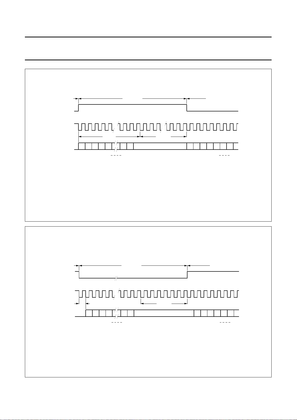
Fig.8 Transfer of SDA data (alternative format).
1716151
MSB
right
4
MLA924 - 2
channel
SWS
SCL
FDAC/
FDAF
bit :
1
2322212
MSB LSB
0
left 32 bits
02010
0
Fig.9 Transfer of FDAF and FDAC (filtered) data.
December 1993 10
7 bits
2322212
MSB
right
0
MLA925 - 2
Page 11

Philips Semiconductors Product specification
Stereo filter and codec SAA2002
channel
SWS
FSYNC
sub-band
LRLLLLLLRRRRRR
31 0 1 31 0 1
Fig.10 SWS related to phase of FSYNC.
Baseband Interface Signals
Table 1 Interface between the SAA2002 and the baseband input/output circuitry.
SIGNAL MODE DESCRIPTION
SWS bi-directional
SCL bi-directional
SDA bi-directional
word (channel) select
bit clock
baseband data
MBC148 - 1
OPERATING
FREQUENCY
f
s
64f
s
−
FDIR output
decoding mode (direction control)
The SWS signal indicates the channel of the sample signal
(either Left or Right) and is equal to the sampling
frequency fs.
Operating at a frequency of 64 x fs that is used for
sampling, the bit clock dictates that each SWS period
contains 64 SDA data bits. Of these, a maximum of 36 are
used to transfer data (samples may have a length up to
December 1993 11
−
18-bits). Samples are transferred most significant bit
(MSB) first. Both SWS and SDA change state at the
negative edge of SCL.
This baseband data is transferred between the SAA2002
and the input/output using either standard I2S (default) or
the alternative format shown in Fig.8.
Page 12

Philips Semiconductors Product specification
Stereo filter and codec SAA2002
Interface between SAA2002 and SAA2012
2
Table 2 Filtered I
S interface.
SIGNAL MODE DESCRIPTION
SWS bi-directional word select (common to I
2
S) f
s
SCL bi-directional bit clock (common to I2S) 64f
FDAC bi-directional codec data −
FDAF bi-directional filter data −
FSYNC output synchronization fs/32
Filtered data is transferred between SAA2002 filter/codec
functions and the SAA2012 using the format shown
in Fig.9.
PASC CODED INTERFACE
The interface that carries the P ASC coded signal uses the
signals as indicated in Table 3.
The frequency of the SWS signal is equal to the sample
frequency fs and the bit clock SCL is 64 times the sample
frequency. Each period of SWS contains 64 data-bits, 48
of which are used to transfer data. The half period in which
Table 3 The PASC I
SIGNAL MODE DESCRIPTION
2
S interface.
SWS is LOW is used to transfer the information of the Left
channel while the following half period during which SWS
is HIGH carries the data of the Right channel. The 24-bit
samples are transferred Most Significant Bit (MSB) first.
This bit is transferred in the bit clock period with a 1-bit
delay following the change in SWS. Both SWS and FDAF/
FDAC change state at the negative edge of SCL.
The SAA2012 may be synchronized to the sub-band
codec using the FSYNC signal, which defines the SWS
period in which the samples of sub-band 0 (containing the
lowest frequency components) are transferred
SBWS bi-directional word selection
SBCL bi-directional bit clock
SBDA bi-directional sub-band coded data
SBEF input error signal
Operation is further controlled by:
• SBDIR: input; direction of data flow
• URDA: input; unreliable encoded data signal.
(see Fig.9).
SAA2012
AND INPUT/OUTPUT MODE CONTROL
The SBMCLK signal is the main frequency from which
other clock signals are derived. In encode mode this
The operation of SAA2012 and the input/output circuitry is
controlled by three signals shown in Table 4.
division is performed internally. In decode mode the
external source should provide SBWS and SBCL. The
frequency of the signal is equal to 1/32nd of the bit rate.
The frequency of the bit clock SBCL is twice that of the
FRESET and SYNCDAI are given whenever:
bit rate.
• FS256, SCL and SWS outputs switch between high and
low impedance
• FS256 frequency is changed
(12.288/11.2896/8.192 MHz)
• FDIR is switching
• The bit rate is changing
• System reset is active.
OPERATING
FREQUENCY
s
December 1993 12
Page 13

Philips Semiconductors Product specification
Stereo filter and codec SAA2002
Table 4 SAA2012 input/output control.
SIGNAL MODE DESCRIPTION
FRESET output request a general reset of SAA2012
FDIR output logic 1 for decoding and logic 0 for encoding mode (common to I2S)
SYNCDAI output pulse for synchronization of digital input/output (TDA1315)
ENCODE MODE
The following modes are supported:
Stereo or 2-channel mono at 384 kbits/s; audio sampling
frequencies of 48, 44.1 and 32 kHz.
ECODE MODE
D
The following modes are supported:
Stereo and joint stereo, 2-channel mono and 1-channel
mono at 384 kbits/s; audio sampling frequencies of 48,
44.1 and 32 kHz.
December 1993 13
Page 14
Philips Semiconductors Product specification
Stereo filter and codec SAA2002
T
FS256
t
fH fL
t
SCL
SWS, SDA, FDAF, FDAC, FSYNC
output
SDA, FDAF, FDAC
input
T
FS256 cycle time (fs = 48 kHz)
FS256 cycle time (fs = 44.1 kHz)
FS256 cycle time (fs = 32 kHz)
T
SCL cycle time
c
t
FS256 HIGH time (fs = 48 kHz)
fH
FS256 HIGH time (fs = 44.1 kHz)
FS256 HIGH time (f
t
FS256 LOW time (fs = 48 kHz)
fL
= 32 kHz)
s
FS256 LOW time (fs = 44.1 kHz)
FS256 LOW time (fs = 32 kHz)
t
SCL HIGH time
sH
t
SCL LOW time
sL
t
SDA, FDAF and FDAC input set-up time
su
before FS256 HIGH
t
SDA, FDAF and FDAC input hold time
h1
after FS256 HIGH
t
SDA, FDAF and FDAC output hold time
h2
after FS256 HIGH
t
FS256 HIGH to SCL, SWS, SDA, FDAF
d1,2
and FDAC output valid
t
d1
t
sL
t
h2
t
d2
t
d1
t
T
c
t
t
h1
su
sH
MEA642 - 3
81.4 ns nominal
88.6 ns nominal
122.1 ns nominal
4T ns nominal
≥ 35 ns
≥ 38 ns
≥ 75 ns
≥ 15 ns
≥ 38 ns
≥ 75 ns
≥ 2T − 20 ns
≥ 2T − 20 ns
≥ 20 ns
≥ 30 ns
≥ 0ns
≤ 50 ns
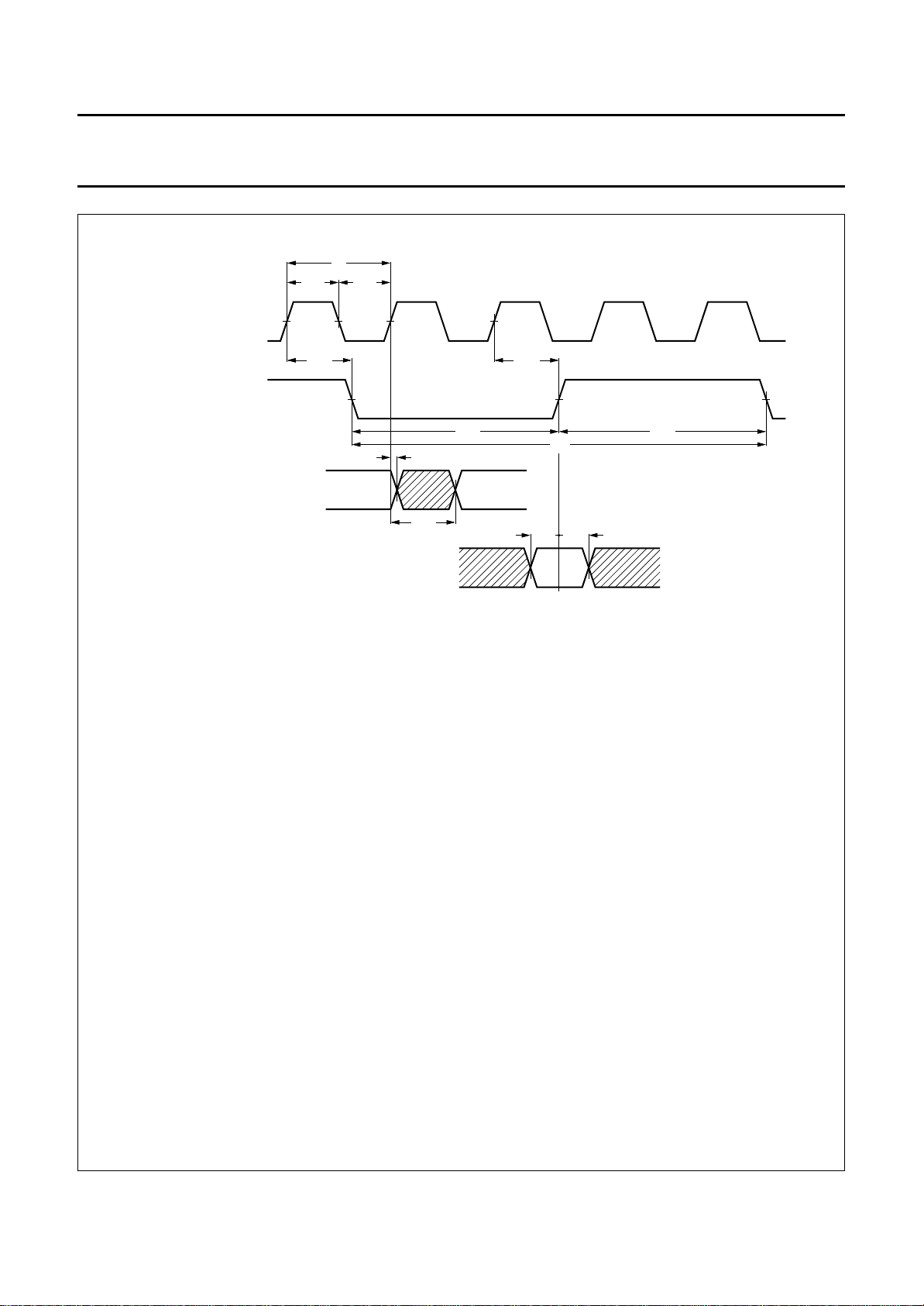
Fig.11 Filtered-I2S interface timing (master mode - FS256, SCL and SWS are output).
December 1993 14
Page 15
Philips Semiconductors Product specification
Stereo filter and codec SAA2002
T
FS256
SCL
SDA, FDAF, FDAC, FSYNC
output
t
t
sH
t
h1
T
t
d
t
fL
c
fH
t
sL
SWS, SDA, FDAF, FDAC
input
t
FS256 HIGH time
fH
t
FS256 LOW time
fL
t
SCL HIGH time
sH
t
SCL LOW time
sL
t
SDA, FDAF and FDAC input set-up time
su
valid after SCL HIGH
t
SDA, FDAF and FDAC output hold time
h1
after SCL HIGH
t
SDA, FDAF and FDAC input hold time
h2
after SCL HIGH
t
SCL HIGH to SDA, FDAF and FDAC
d
output valid
≥ 35 ns
≥ 35 ns
≥ T + 35 ns
≥ T + 35 ns
≥ 20 ns
≥ 2T − 15 ns
≥ T + 20 ns
≤ 3T + 60 ns
t
su
t
h2
MEA644 - 3
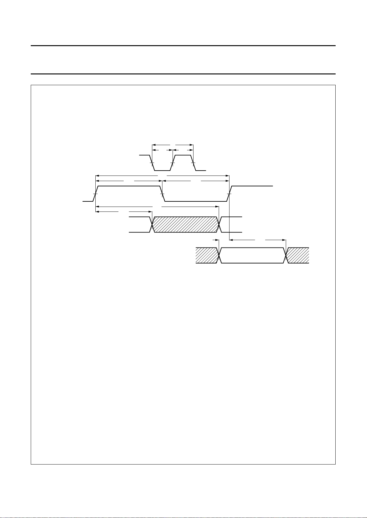
Fig.12 Filtered-I2S interface timing (slave mode - FS256, SCL and SWS are input).
December 1993 15
Page 16
Philips Semiconductors Product specification
Stereo filter and codec SAA2002
FRESET
SYNCDAI
FDIR
SDA
FDAF
FDAC
t
d0
t
t
d3
d2
t
d4
HIGH Z
t
d6
HIGH Z
t
d7
HIGH Z
SWS
FS256
SCL
t
sH
t
FDAF
FDAC
t
d1
t
d5
HIGH Z
HIGH Z
d8
HIGH Z
t
d9
SWS
FS256
SCL
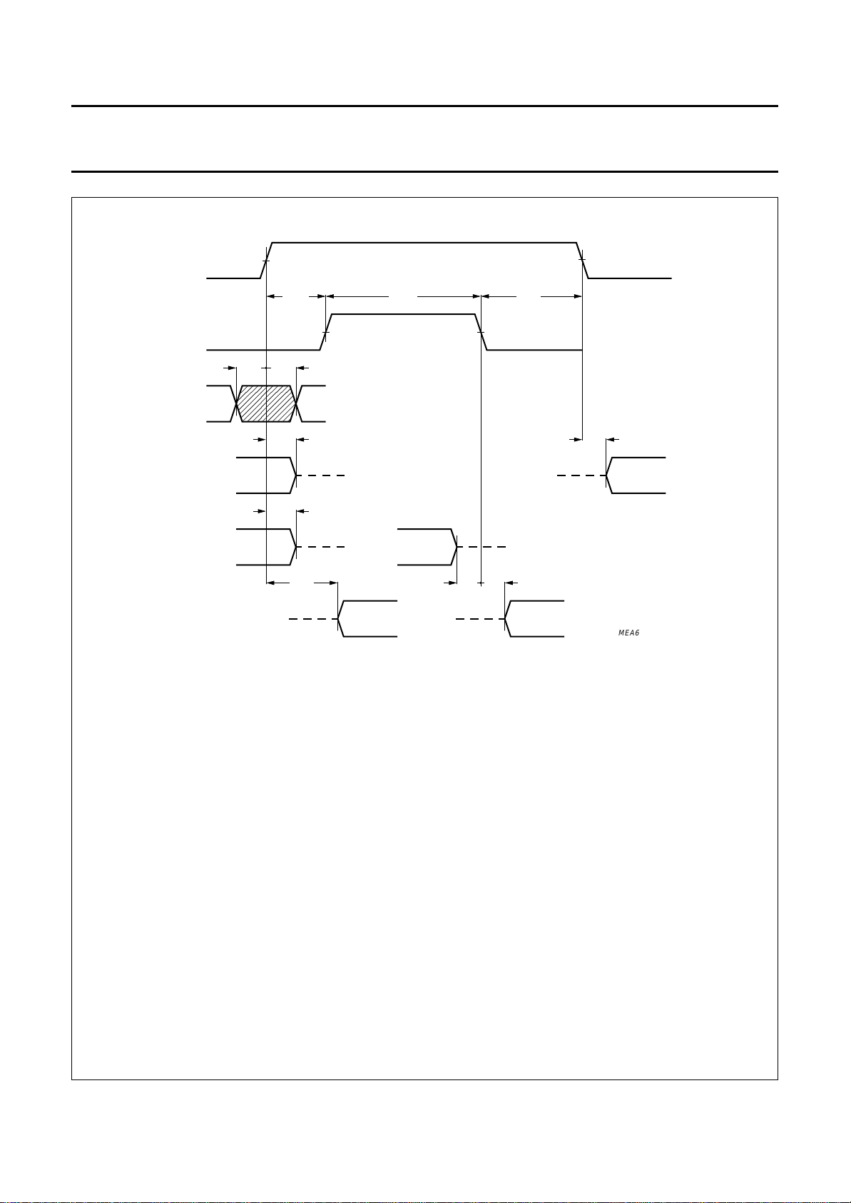
MEA646 - 1
SDA
t
FRESET HIGH to SYNCDAI HIGH
d0
t
SYNCDAI HIGH time
sH
t
SYNCDAI LOW to FRESET LOW
d1
t
FDIR hold to FRESET HIGH
d2
t
FRESET HIGH to FDIR valid
d3
t
SDA change to high impedance after FRESET HIGH
d4
t
SDA remains high impedance after FRESET LOW
d5
t
FDAF and FDAC change to high impedance after FRESET
d6
HIGH
t
FDAF and FDAC remain high impedance after FRESET HIGH
d7
t
FS256, SWS and SCL change to high impedance before
d8
SYNCDAI HIGH
t
FS256, SWS and SCL remain high impedance after
d9
SYNCDAI HIGH
Fig.13 Mode switch timing.
December 1993 16
≥ 300 ns
≥ 1280 ns
≥ 790 ns
≤ 20 ns
≤ 20 ns
≥ 0 ns and ≤ 170 ns
≥ 0 ns and ≤ 170 ns
≤ 20 ns
≥ 460 ns
≥ 140 ns
≥ 140 ns
Page 17
Philips Semiconductors Product specification
Stereo filter and codec SAA2002
32 bits
SBWS
SBCL
SBDA
bit :
SBEF
0001020
15 bits1
3
byte 0 byte 1 byte 2
10111
2
13141
LSBMSB
5
1
16171
MSB
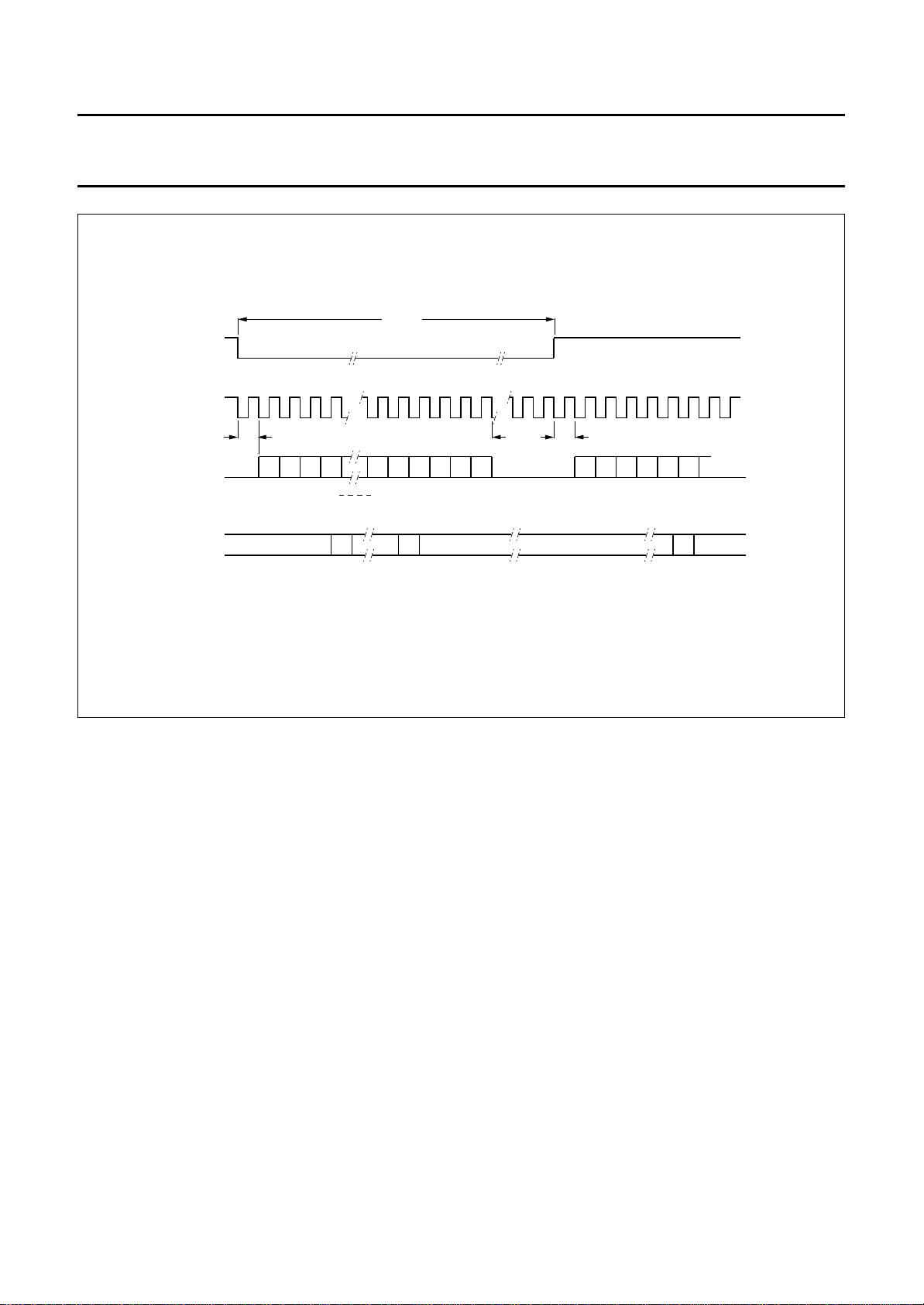
Fig.14 Transferring PASC data to and from the SAA2002.
202
1
8
9
1
MEA649 - 2
2
2
December 1993 17
Page 18
Philips Semiconductors Product specification
Stereo filter and codec SAA2002
E
PASC Coded Interface (sub-band I2S)
NCODING MODE
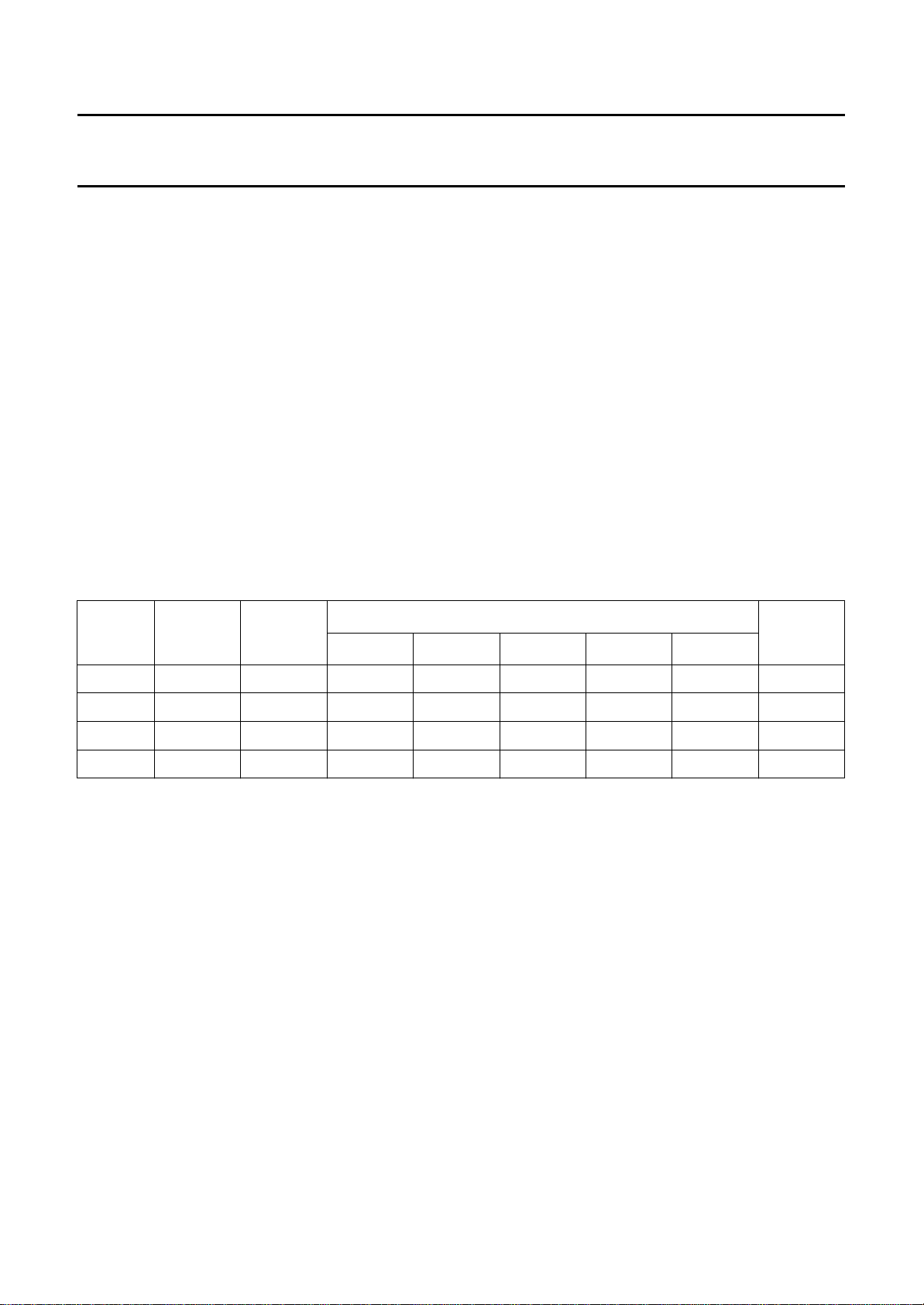
The PASC coded data is transferred to and from the
SAA2002 using the format shown in Fig.15.
Each period of SBWS contains 64 data bits, 32 of which
are used to convey data. The half-period during which
SBWS is logic 0 is used to transfer the first 16-bits (0 to 15)
of a sub-band slot. The remaining half-period during which
SBWS is logic 1 carries the remaining 16-bits (16 to 31).
Thus one period of SBWS corresponds with one slot of the
sub-band signal.
Bits 0 and 16 are transferred in the bit clock period, one
bit-time after the change in SBWS. Both SBWS and SBDA
change state during the negative edge of SBCL.
In decode mode a byte error flag SBEF is also transferred.
This occurs approximately in the middle of the
corresponding byte (byte 0 = bits 0 to 7,
byte 1 = bits 8 to 15 etc.).
Table 5 Modes and source signals.
MODE FDIR SBDIR
SBWS SBCL SBDA SBEF SBMCLK
Encode 0 0 INT INT INT − − − INT note 1
SBCL, SBWS and SBDA are generated by the SAA2002.
However, if the SBDIR signal is logic 1, the output buffers
are not enabled and these signals do not appear on the
pins. This mode is available to permit a change of
operating mode whilst the bus signals are driven from an
external source.
ECODING MODE
D
SBCL, SBWS and SBDA are generated by an
external source.
Table 5 contains a summary of the source signals in the
various modes.
SOURCE
REMARKS
Encode 0 1 EXT EXT EXT − − − INT note 2
Decode 1 0 INT INT INT EXT INT note 3
Decode 1 1 EXT EXT EXT EXT INT
Notes
1. During encoding the SBEF signal is ’don’t care’.
2. Incoming data is not decoded. The SAA2002 operates in the encoding mode and the data does not enter the interface.
3. Operation is undefined. The SAA2002 is in decoding mode whilst the SBWS, SBCL and SBDA output drivers are enabled.
December 1993 18
Page 19
Philips Semiconductors Product specification
Stereo filter and codec SAA2002
T
s
SBMCLK
SBCL
SBWS
SBDA
t
t
cL
t
t
d2
d1
T
mL
sc
t
mH
t
cH
MEA645 - 2
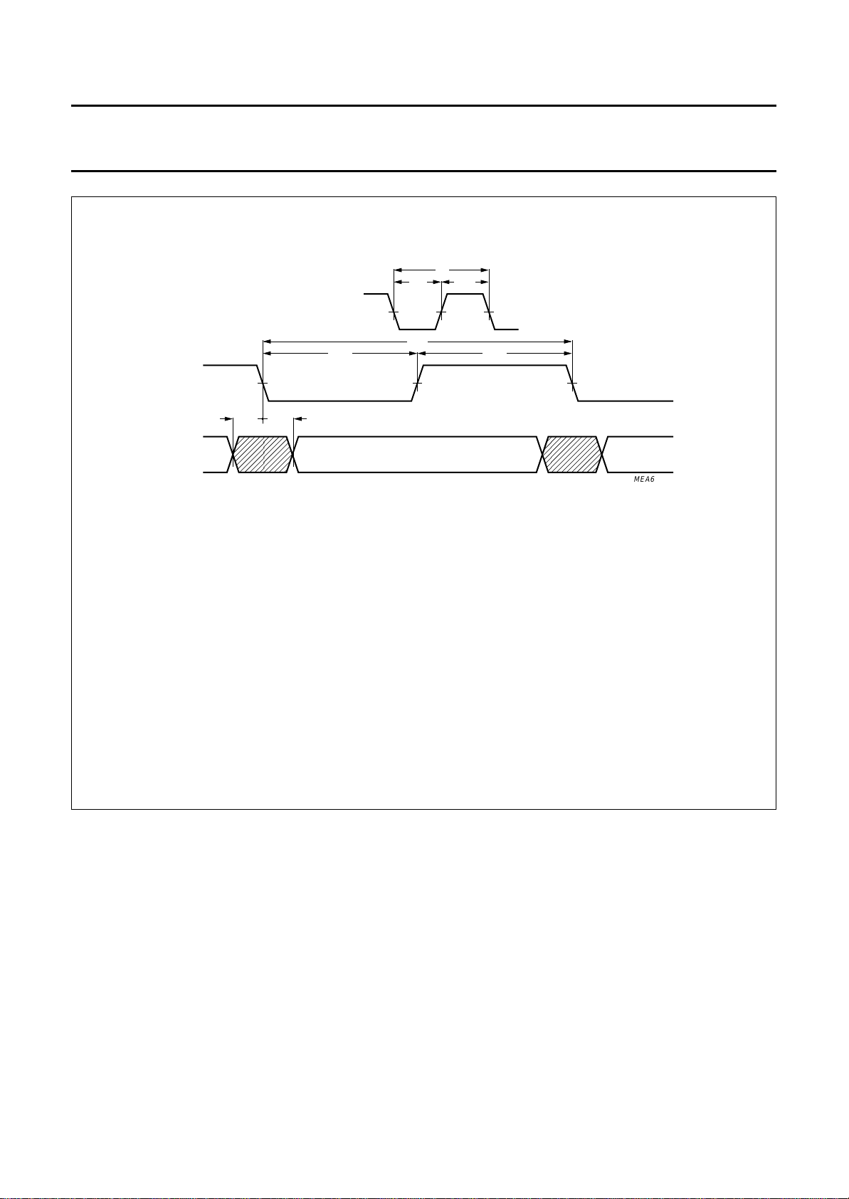
T
SBMCLK cycle time
s
t
SBMCLK HIGH time
mH
t
SBMCLK LOW time
mL
T
SBCL cycle time (384 kbits/s)
sc
t
SBCL HIGH time (384 kbits/s)
cH
t
SBCL LOW time (384 kbits/s)
cL
t
SBWS, SBDA hold to SBCL LOW
d1
t
SBCL LOW to SBWS, SBDA valid
d2
Fig.15 Sub-band I2S interface timing (master mode - SBCL, SBWS and SBDA are output).
120 to 205 ns (163 ns nominal)
≥ 35 ns
≥ 75 ns
8Ts ns nominal
≥ 4Ts− 20 ns
≥ 4Ts− 20 ns
≤ 20 ns
≤ 20 ns
December 1993 19
Page 20
Philips Semiconductors Product specification
Stereo filter and codec SAA2002
SBWS
SBCL
SBDA
SBEF
SBCL
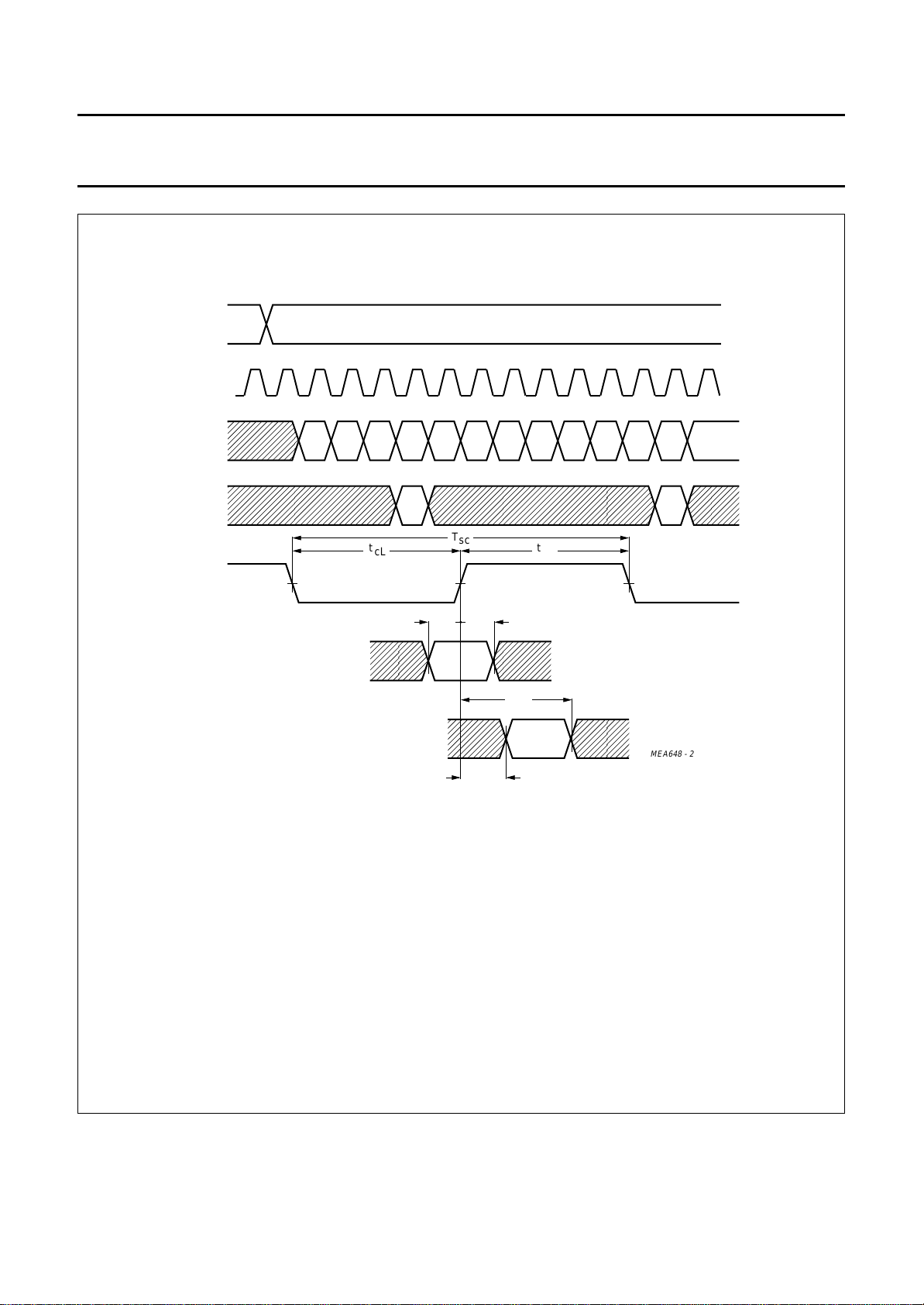
SBMCLK cycle time
T
s
SBCL cycle time
T
sc
SBCL HIGH time
t
cH
SBCL LOW time
t
cL
SBWS, SBDA input set-up time
t
su1
before SBCL HIGH
SBWS, SBDA input hold time after
t
h1
SBCL HIGH
SBCL HIGH to SBEF valid
t
su2
SBEF hold time after SBCL HIGH
t
h2
0 1 2 3 4 5 6 7 8 9 10 11 12
T
t
su1
sc
t
h1
t
su2
t
cH
t
h2
MEA648 - 2
SBWS
SBDA
SBEF
t
cL
8Ts ns nominal
≥ Ts + 30 ns
≥ Ts + 30 ns
≥ Ts + 30 ns
≥ 30 ns
≤ Ts− 30 ns
≥ 2Ts− 30 ns
Fig.16 Sub-band I2S interface timing (slave mode - SBCL, SBWS and SBDA are input).
December 1993 20
Page 21
Philips Semiconductors Product specification
Stereo filter and codec SAA2002
SBDIR
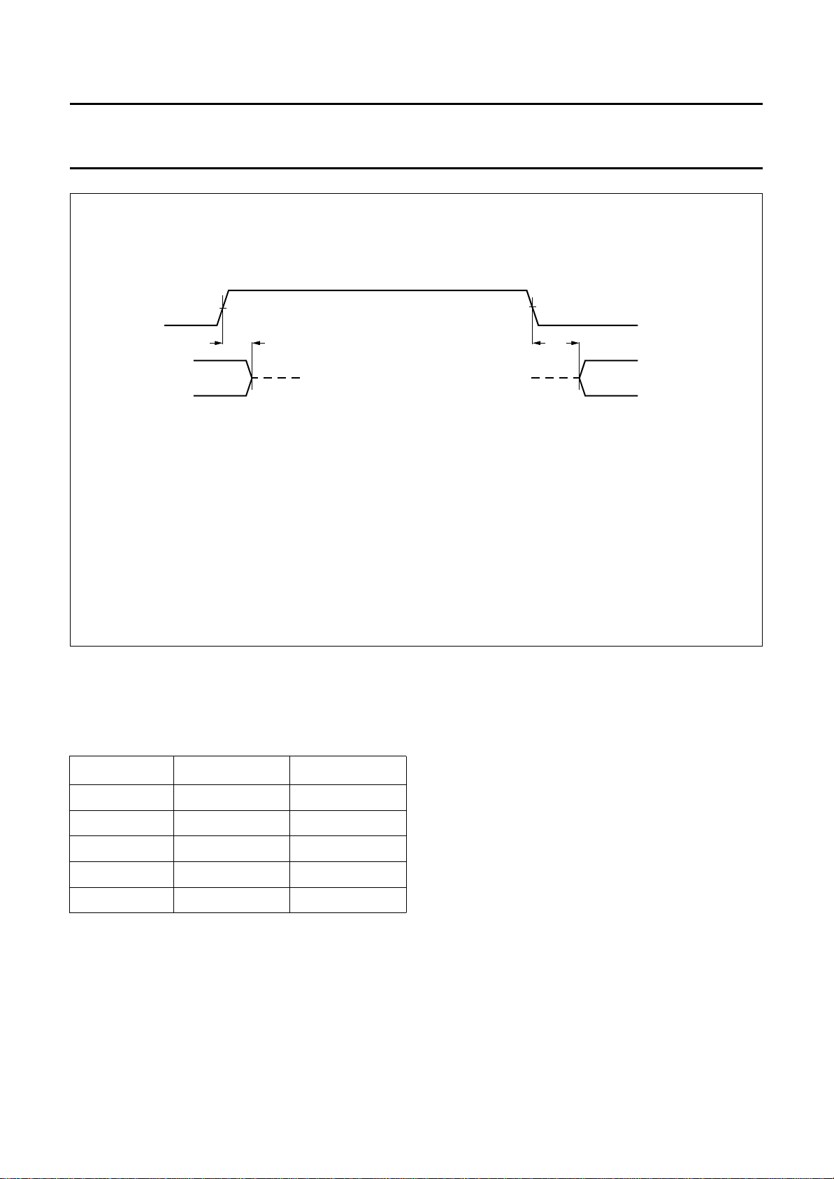
t
d1
HIGH Z
t
SBDIR HIGH to SBCL, SBWS
d1
SBDA high impedance
t
SBCL SBWS, SBDA low impedance
d2
after SBDIR LOW
≤ 50 ns
≥ 240 ns
Fig.17 Sub-band I2S mode switch timing.
Microcontroller interface
The SAA2002 has an interface connection to the serial
interface of a microcontroller.
Table 6 Signals used.
SIGNAL DIRECTION DESCRIPTION
LTCLK input bit clock
LTDATA bi-directional serial data
LTCNT0 input control line 0
LTCNT1 input control line 1
LTENSFC input enable
The SAA2002 microcontroller interface is enabled only if
LTENSFC (pin 34) is logic 1. Information to or from the
SAA2002 is conveyed in serial 8 or 16-bit units, whilst the
type of information is controlled by LTCNT0 (pin 35) and
LTCNT1 (pin 36).
t
d2
HIGH Z
MEA647 - 1
SBCL
SBWS
SBDA
A transfer commences when the microcontroller sets the
control lines to the correct combination for the required
action. LTENSFC is set to logic 1. The SAA2002
determines its required action and prepares to transfer
data. When the microcontroller supplies the LTCLK, data
is transferred to or from the SAA2002 in units of 8-bits.
16-bit transfers are conveyed as two 8-bit units during
which LTENSFC remains HIGH.
During the transfer of 8-bit units, the least significant bit is
first to be transferred. When 16-bit units are transferred the
most significant byte is sent first
XTENDED SETTINGS (LTCNT1 = LOGIC 0,
E
LTCNT0 =
LOGIC 0)
Four information bits together with four address bits are
transferred in this mode. The order in which the bits appear
on the interface is:
D0 .. D1 .. D2 .. D3 .. A0 .. A1 .. A2 .. A3
December 1993 21
Page 22
Philips Semiconductors Product specification
Stereo filter and codec SAA2002
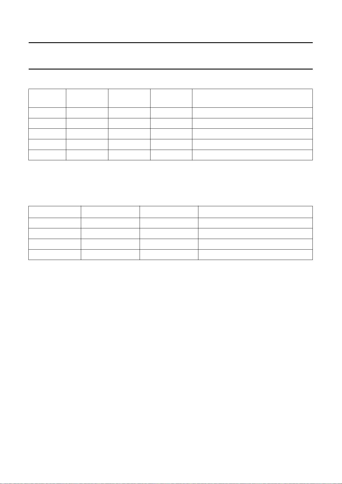
Table 7 Extended settings.
BIT
A3
BIT
A2
BIT
A1
BIT
A0
DESCRIPTION
0 0 0 0 CODEC external settings; see Table 8
0 0 0 1 FILTER settings; note 1
0 0 1 0 not used
.. .. .. .. ..
1 1 1 1 not used
Note
1.When D0 = logic 1 (default) I2S mode is selected. For D0 = logic 0 the alternative mode is selected. The setting of D0
remains dormant until activated by the occurrence of FRESET.
Table 8 Extended settings.
BIT DESIGNATION DEFAULT DESCRIPTION
D0 MUTEDAC
D1 ATTDAC
D2 DEEMDAC
(1)
(1)
(1)
1 connected to DAC mute input
0 connected to DAC attenuation input
0 emphasis control for DAC circuit
D3 HOLDCLKOK 0 selects CLKOK hold mode
Note
1.If not used for DAC control, the MUTEDAC, ATTDAC and DEEMDAC can be used as general purpose output
expanders.
Bits D0 to D3 are copied directly to the corresponding
output pins/mode flip-flop.
For HOLDCLKOK = logic 1. When CLKOK drops it will
remain low until set by an encode/decode mode, sample
frequency, external 256FS or bit rate index change.
LLOCATION/SCALE FACTOR INFORMATION
A
(LTCNT1 = LOGIC 0, LTCNT0 = LOGIC 1)
For recording, the allocation and scale factor arrays can be
filled using this mode. To completely fill the allocation array
16 complete transfers of 16-bits are required. After the first
transfer of allocation information a check must be made to
determine when the SAA2002 is ready to receive the
remaining information. This will ensure synchronization
with the internal program of the SAA2002. Transfer of the
allocation information is completed by sending the
In the event that only internal settings information is sent,
then a default allocation of logic 0 will be assigned to all
sub-bands. If, in addition no internal settings are sent, then
the previous settings remain valid.
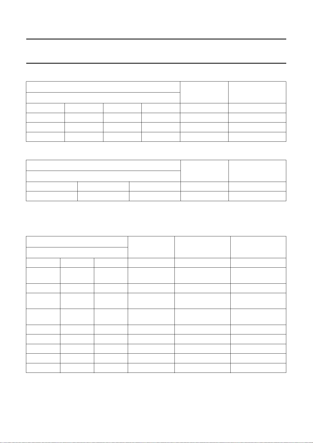
The allocation information is transferred in 4-bit units.
Each of these units contains the number of bits allocated
to the sub-band, MINUS 1, except in the case of a logic 0
value, which indicates that no bits are allocated to that
sub-band.
Scale factor information is transferred in units of 8-bits,
containing the 6-bit scale factor which is extended to 8- bits
by adding two logic 0s at the most significant end.
In the case of stereo encoding the channels are indicated
by L (left) and R (right). This changes to I and II in the case
of 2 channel mono encoding.
internal settings.
This is then followed by the scale factor information.
December 1993 22
Page 23
Philips Semiconductors Product specification
Stereo filter and codec SAA2002
Table 9 Allocation information format.
BITS
CHANNEL SUB-BAND
MSB LSB
B15 B14 B13 B12 L or I 0, 2, 4, .... 30 (even)
B11 B10 B9 B8 R or II 0, 2, 4, .... 30 (even)
B7 B6 B5 B4 L or I 1, 3, 5, .... 31 (odd)
B3 B2 B1 B0 R or II 1, 3, 5, .... 31 (odd)
Table 10 Scale factor information format.
BITS
CHANNEL SUB-BAND
MSB LSB
B15 to B8 L or I 0 to 31
B7 to B0 R or II 0 to 31
INTERNAL SETTINGS (LTCNT1 = LOGIC 1, LTCNT0 = LOGIC 0)
The operation of the codec is controlled by the bits transferred in this mode.
Table 11 Internal settings (LTCNT1 =
BITS
MSB LSB
S15 to S12 bit rate index bit rate indication encode
S11 to S10 sample frequency 44.1, 48 or 32 kHz
S9 −−decode 1 = decode, 0 = encode encode/decode
S8 −−EXT 256FS 1 = external;
S7 −−2-channel mono 1 = 2-channel mono;
S6 −−MUTESFC 1 = mute; 0 = no mute encode/decode
LOGIC 1, LTCNT0 = LOGIC 0).
NAME FUNCTION VALID IN
encode
indication
encode/decode
0 = internal 256FS
encode
0 = stereo
S5 −− not used −
S4 −−CH1 1 = CH1; 0 = CH2 decode
S3 to S2 Tr0 to Tr1 transparent bits encode
S1 to S0 EMPHASIS emphasis indication encode
December 1993 23
Page 24
Philips Semiconductors Product specification
Stereo filter and codec
Table 12 Internal settings (LTCNT1 = LOGIC 1, LTCNT0 = LOGIC 0).
BITS
BIT RATE REMARK
MSB LSB
1 1 0 0 384 kbits/s default value
The bit rate index indicates the bit rate of the encoded
signal and is only effective in the encode mode.
The decode bit determines the operation mode of the
SAA2002. The default value is 1 (decoding mode).
EXT 256FS in the encoding mode determines whether or
not the SAA2002 is master or slave of the Filtered-I2S
interface (default is 0, master mode).
2-channel mono is used in the encoding mode to
determine whether the sub-band signal is generated as a
stereo or 2-channel mono signal. Default value is 0.
MUTESFC is used in both the encoding and decoding
modes to mute the information to or from the Filtered-I2S
interface (the default value is 0).
CH1 is utilized in the decoding mode to select one of the
2-channel mono signals to be decoded (default is 1
channel 1). A value of 0 results in channel 2 being
decoded.
The transparent bits are copied in the sub-band signal,
default is 00.
The information from S15 to S10, S7 and S3 to S0 will be
copied into the sub-band signal.
SAA2002
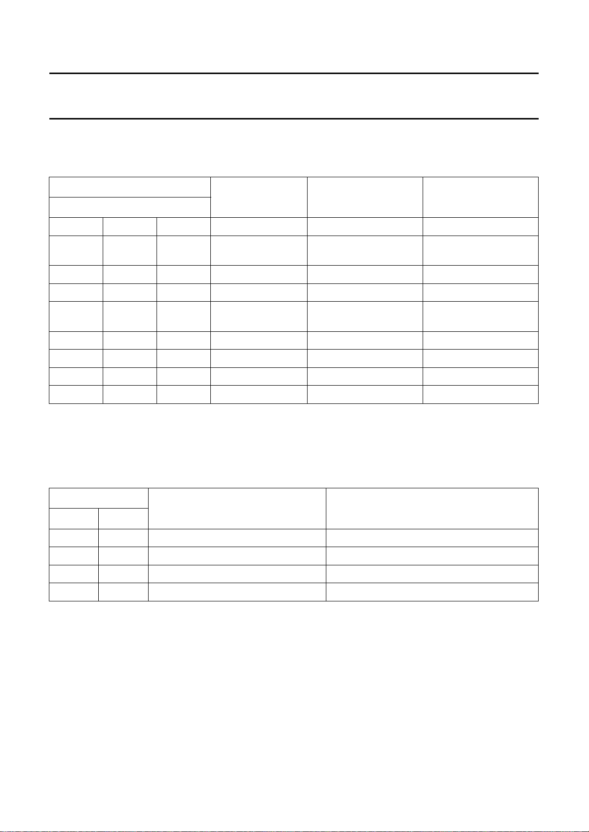
Table 13 Sample frequency indication.
BITS
SAMPLE FREQUENCY REMARK
MSB LSB
0 0 44.1 kHz default value
0 1 48 kHz −
1 0 32 kHz −
1 1 not used −
Table 14 EMPHASIS indication.
BITS
EMPHASIS REMARK
MSB LSB
0 0 no emphasis default value
0 1 50/15 µs −
1 0 reserved −
1 1 CCITT J.17 −
Before sending internal settings the microcontroller should check whether or not the SAA2002 is ready-to-receive.
However, this does not apply for the transfer of internal settings to end a transfer of allocation information.
December 1993 24
Page 25
Philips Semiconductors Product specification
Stereo filter and codec SAA2002
STATUS (LTCNT1 = LOGIC1, LTCNT0 = LOGIC 1)
Table 15 Status information 16-bits units.
BITS
NAME FUNCTION VALID IN
MSB LSB
T15 to T12 bit rate index bit rate indication encode/decode
T11 to T10 sample frequency 44.1, 48 or 32 kHz
indication
T9 −−ready-to-receive 1 = ready, 0 = not ready encode/decode
T8 −−not used
T7 to T6 MODE sub-band signal mode
indication
T5 −−SYNC synchronization indication decode
T4 −−CLKOK 1 = OK; 0 = not OK encode/decode
T3 to T2 Tr0 to Tr1 transparent bits encode/decode
T1 to T0 EMPHASIS emphasis indication encode/decode
The bit rate index indicates the bit rate of the sub-band signal in units of 32 kbits/s. Bit rate index 0000 indicates the 'free
format' condition. Bit rate 1111 is illegal and should not be found.
The coding of the sample frequency indication is equal to the one in the internal settings.
Table 16 MODE identification.
BITS
MODE OUTPUT
MSB LSB
encode/decode
encode/decode
0 0 stereo L and R
0 1 joint stereo L and R
1 0 2-channel mono I or II; as selected
1 1 1-channel mono mono; no selection
December 1993 25
Page 26

Philips Semiconductors Product specification
Stereo filter and codec SAA2002
Ready-to-receive indicates whether the SAA2002 is ready
to receive allocation, scale factor or internal setting
transfers. This should be checked in order to synchronize
the transfer of such information.
In 2-channel mono decode mode the selected samples are
transferred to both output channels. The same occurs with
all samples in 1-channel mono decode mode. In both of
these cases the L and R filter output channels are
identical.
In decode mode the SYNC bit is logic 0 when the SAA2002
is unable to decode the sub-band frames. This will occur in
the following situations:
• With the loss of synchronization.
• When the incorrect allocation information is received for
two or more subsequent frames (SBEF was HIGH).
• When the URDA input pin (6) is HIGH.
In these situations the SAA2002 data output will be muted.
The SYNC bit will return to logic 1 as soon as the decoder
is re-synchronized to the incoming sub-band data.
CLKOK indicates whether the 256FS clock corresponds to
specified sample frequency. The CLKOK bit is set to
logic 1 after a change in sample frequency, operation
mode or EXT256FS setting. It drops to logic 0 as soon as
the 256FS clock deviates from the nominal frequency by
more than approximately 0.2%. Return to logic 1 will only
occur automatically when the extended setting
CLKOK-hold-mode is logic 0.
The transparent bits are copied from the PASC signal.
The EMPHASIS indication is as defined in the internal
settings. It can be used to apply the correct de-emphasis.
Remark: The two bytes of the status are 'sampled' at
different moments so the information may not result from
the same sub-band frame.
December 1993 26
Page 27
Philips Semiconductors Product specification
Stereo filter and codec SAA2002
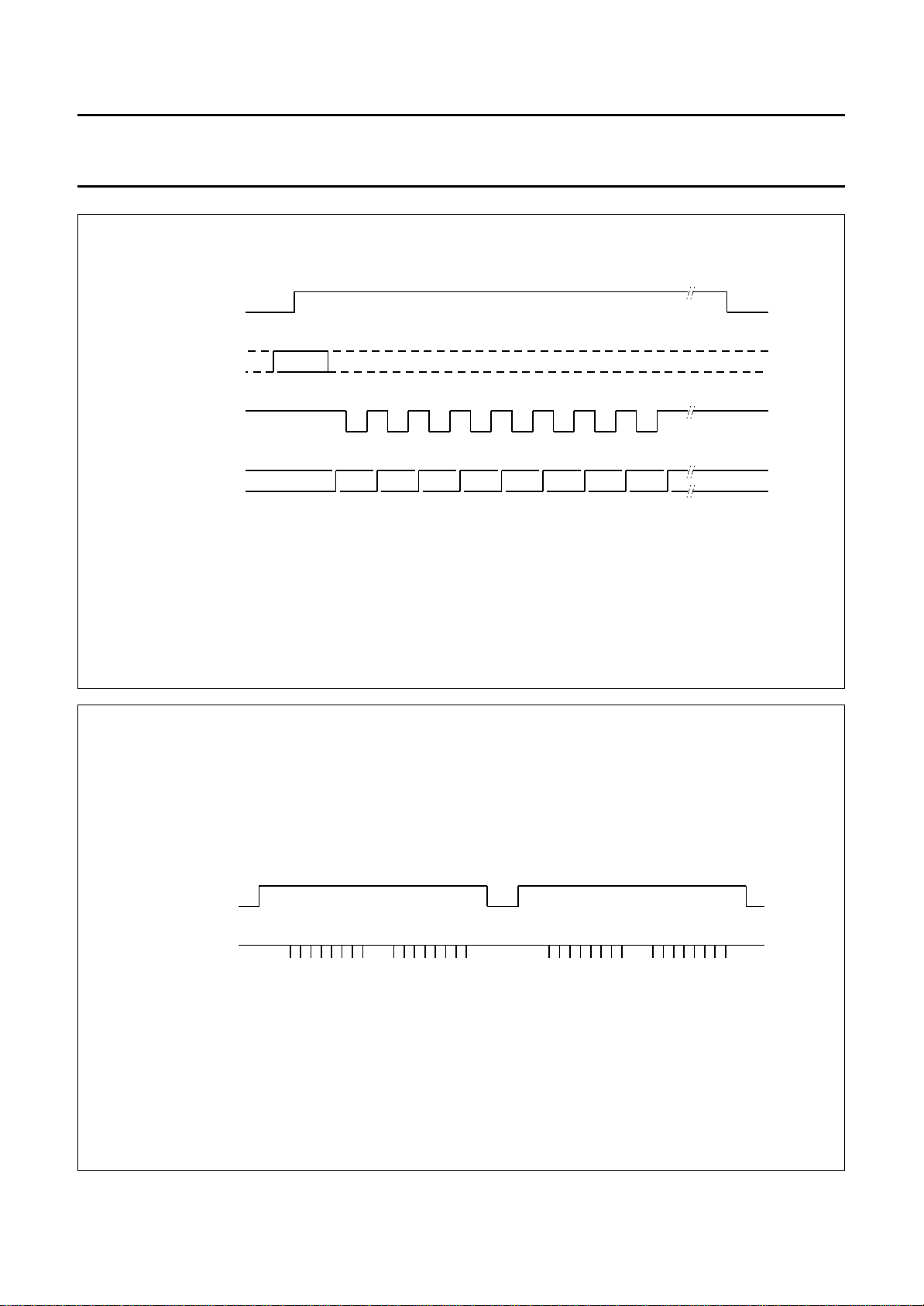
LTENSFC
LTCNT0/1
LTCLK
LTDATA
01234567
LSB MSB
MLA933 - 1
LTENSFC
LTCLKC
Fig.18 Transfer of data on the SAA2002 microcontroller interface.
16 bits allocation / scale factor information 16 bits allocation / scale factor information
MEA650
December 1993 27
Fig.19 The LTENSFC line must return to logic 0 between information transfers.
Page 28
Philips Semiconductors Product specification
Stereo filter and codec SAA2002
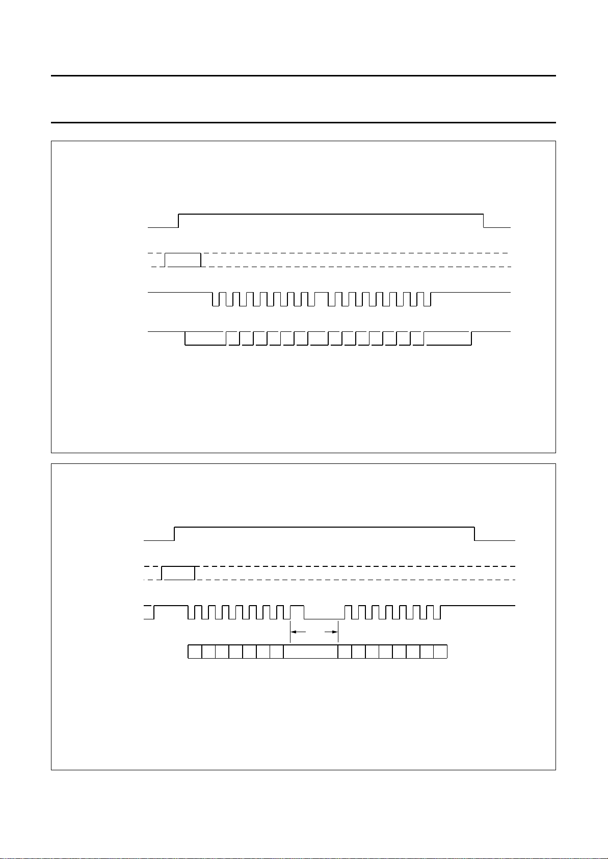
LTENSFC
LTCNT0/1
LTCLK
LTDATA
bit :
8
1011121314 0
9
2
4
1
3
6
5
715
MEA651
Fig.20 Order of settings and status bits on the SAA2002 microcontroller interface.
LTENSFC
LTCNT0/1
LTCLK
LTDATA
OUTPUT
8 9 10 11 12 13 14 15 0 1 2 3 4 5 6 7
LTENSFC must remain HIGH
t
d6
td6 delay time LTCLK HIGH to LTDATA valid output for bit 0 in 16-bit transfers.
MEA653 - 2
December 1993 28
Fig.21 16-bit transfers.
Page 29
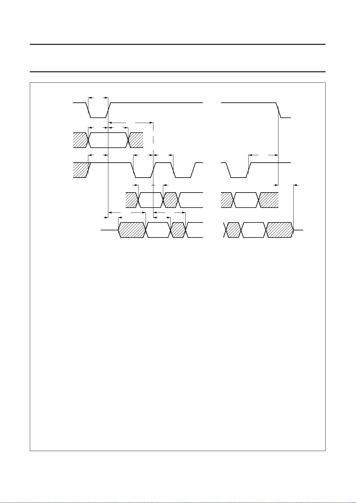
Philips Semiconductors Product specification
Stereo filter and codec SAA2002
t
eL
LTENSFC
t
d1
t
h1
t
cL
LTCNT0
LTCNT1
t
cH
t
h4
LTCLK
t
t
su1
d5
LTCDATA
input
t
d3
t
d2
LTCDATA
output
t
LTENSFC LOW time
eL
t
LTCLK HIGH time
cH
t
LTCLK LOW time
cL
t
LTENSFC HIGH to LTCLK HIGH
d1
t
LTENSFC HIGH to LTDATA output low
d2
HIGH Z
impedance
t
LTENSFC HIGH to LTDATA output valid
d3
t
LTENSFC LOW to LTDATA high impedance
d4
t
LTENSFC hold time after LTCLK HIGH
h4
t
LTCLK HIGH to LTENSFC HIGH
d5
t
LTCLK HIGH to LTDATA output valid;
d6
for bit 0 (see Fig.21)
for bit 8
t
LTCNT0/1 set-up time before LTENSFC HIGH
su1
t
LTCNT0/1 hold time after LTENSFC HIGH
h1
t
LTDATA set-up time before LTCLK HIGH
su2
t
LTDATA input hold time after LTCLK HIGH
h2
t
LTDATA output hold time after LTCLK HIGH
h3
t
LTENSFC hold time after LTCLK HIGH
h4
t
su2
t
h3
t
h2
t
d6
≥ 190 ns
≥ 190 ns
≥ 190 ns
≥ 190 ns
≥ 0ns
≤ 380 ns
≤ 50 ns
≥ 355 ns
≥ 190 ns
≤ 355 ns
≤ 520 ns
≥ 190 ns
≥ 190 ns
≥ 190 ns
≥ 30 ns
≥ 145 ns
≥ 355 ns
t
d4
MEA643 - 1
HIGH Z
December 1993 29
Fig.22 Microcontroller interface timing.
Page 30
Philips Semiconductors Product specification
Stereo filter and codec SAA2002
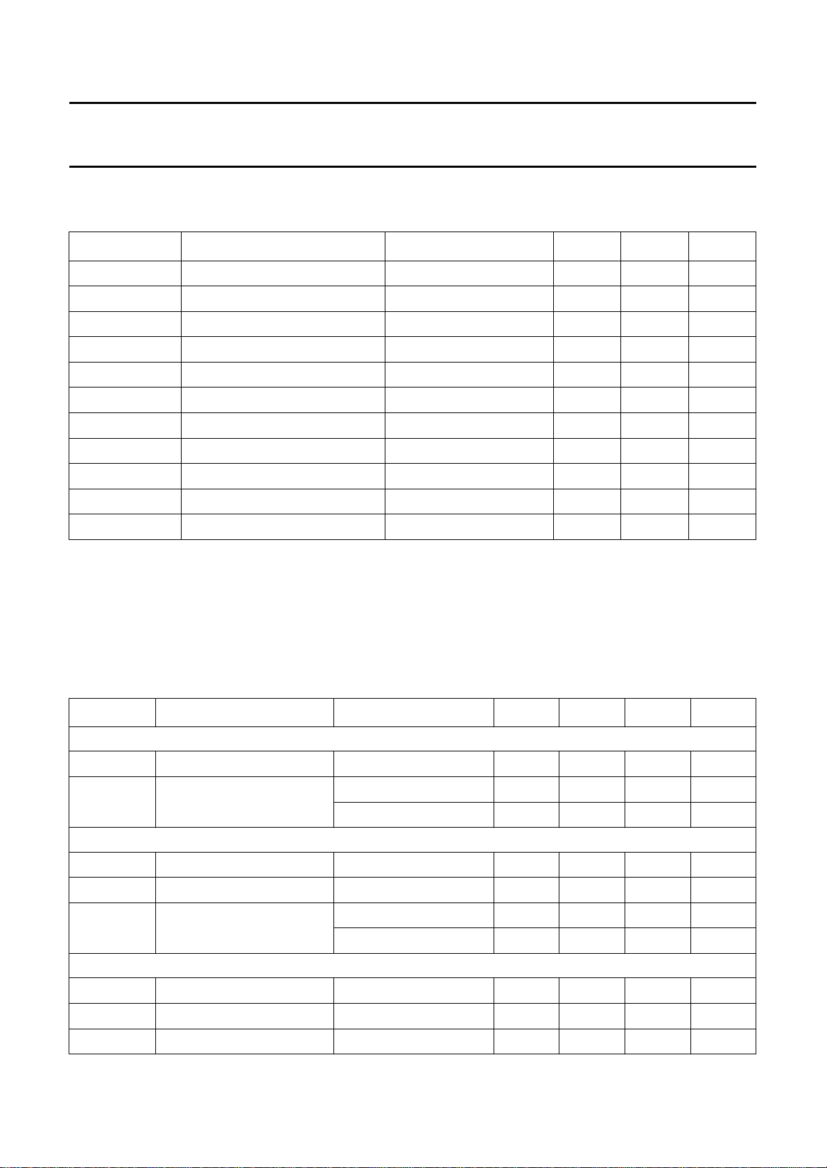
LIMITING VALUES
In accordance with the Absolute Maximum Rating System (IEC 134).
SYMBOL PARAMETER CONDITIONS MIN. MAX. UNIT
V
DD
V
I
I
SS
I
DD
I
I
I
O
P
tot
T
stg
T
amb
V
es1
V
es2
supply voltage −0.5 +6.5 V
input voltage note 1 −0.5 VDD + 0.5 V
supply current in V
supply current in V
SS
DD
input current −10 +10 mA
output current −20 +20 mA
total power dissipation − 880 mW
storage temperature −55 +150 °C
operating ambient temperature −40 +85 °C
electrostatic handling note 2 −1500 +1500 V
electrostatic handling note 3 −70 +70 V
Notes
1. Input voltage should not exceed 6.5 V unless otherwise specified.
2. Equivalent to discharging a 100 pF capacitor through a 1.5 kΩ series resistor.
3. Equivalent to discharging a 200 pF capacitor through a 0 Ω series resistor.
DC CHARACTERISTICS
= 3.8 to 5.5 V; T
V
DD
= −40 to +85 °C; unless otherwise specified.
amb
− 160 mA
− 160 mA
SYMBOL PARAMETER CONDITIONS MIN. TYP. MAX. UNIT
Supply
V
DD
I
DD
supply voltage note 1 3.8 5.0 5.5 V
supply current VDD= 5 V; note 2 − 82 110 mA
= 3.8 V; note 2 − 58 80 mA
V
DD
Inputs URDA, SBDIR, SBEF, LTCLK, LTCNT0, LTCNT1, X22IN and X24IN
V
IL
V
IH
I
I
LOW level input voltage −−0.3V
HIGH level input voltage 0.7V
input current VI = 0 V; T
= 5.5 V; T
V
I
= 25 °C −−−10 µA
amb
= 25 °C −−10 µA
amb
−−V
DD
DD
V
Inputs PWRDWN and LTENSFC
V
IL
V
IH
I
I
LOW level input voltage −−0.3V
HIGH level input voltage 0.7 V
input current VI = VDD; T
= 25 °C40 − 250 µA
amb
−−V
DD
DD
V
December 1993 30
Page 31
Philips Semiconductors Product specification
Stereo filter and codec SAA2002
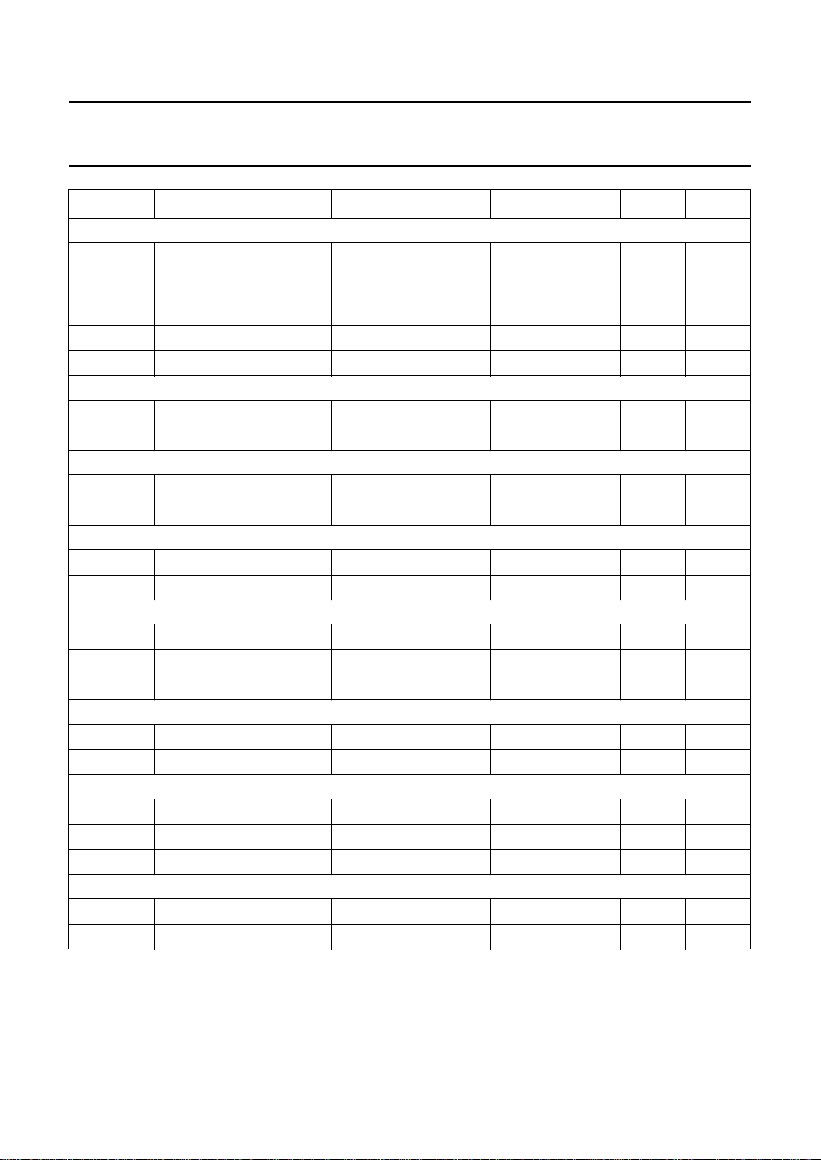
SYMBOL PARAMETER CONDITIONS MIN. TYP. MAX. UNIT
Inputs RESET
V
tLH
threshold voltage
−−0.8V
LOW-to-HIGH
V
tHL
threshold voltage
0.2V
−−V
DD
HIGH-to-LOW
V
hys
I
I
hysteresis V
input current VI = VDD; T
tLH
− V
tHL
= 25 °C40 − 250 µA
amb
− 1.5 − V
Outputs MUTEDAC, DEEMDAC, ATTDAC, SYNCDAI, FDIR, FRESET, FSYNC and CLK22
V
OL
V
OH
LOW level output voltage IO = −2mA −−0.4 V
HIGH level output voltage IO = 2 mA VDD− 0.5 −−V
Output CLK24
V
OL
V
OH
LOW level output voltage IO = −8mA −−0.4 V
HIGH level output voltage IO = 8 mA VDD− 0.5 −−V
Inputs/outputs SBDA, SBCL, SBWS, FDAF, FDAC, SCL, SWS, SDA and LTDATA
V
OL
V
OH
LOW level output voltage IO = −2mA −−0.4 V
HIGH level output voltage IO = 2 mA VDD− 0.5 −−V
Outputs SBDA, SBCL, SBWS, FDAF, FDAC, SCL, SWS, SDA and LTDATA in 3-state
V
IL
V
IH
I
I
LOW level input voltage −−0.3V
HIGH level input voltage 0.7V
input current VI = VDD; T
= 25 °C40 − 250 µA
amb
−−V
DD
Input/output SBMCLK
DD
DD
V
V
V
OL
V
OH
LOW level output voltage IO = −8mA −−0.4 V
HIGH level output voltage IO = 8 mA VDD− 0.5 −−V
Output SBMCLK in 3-state
V
IL
V
IH
I
I
LOW level input voltage −−0.3V
HIGH level input voltage 0.7V
input current VI = VDD; T
amb
Input/output FS256
V
OL
V
OH
LOW level output voltage IO = −12 mA −−0.4 V
HIGH level output voltage IO = 12 mA VDD− 0.5 −−V
December 1993 31
V
DD
−−V
DD
= 25 °C40 − 250 µA
Page 32
Philips Semiconductors Product specification
Stereo filter and codec SAA2002
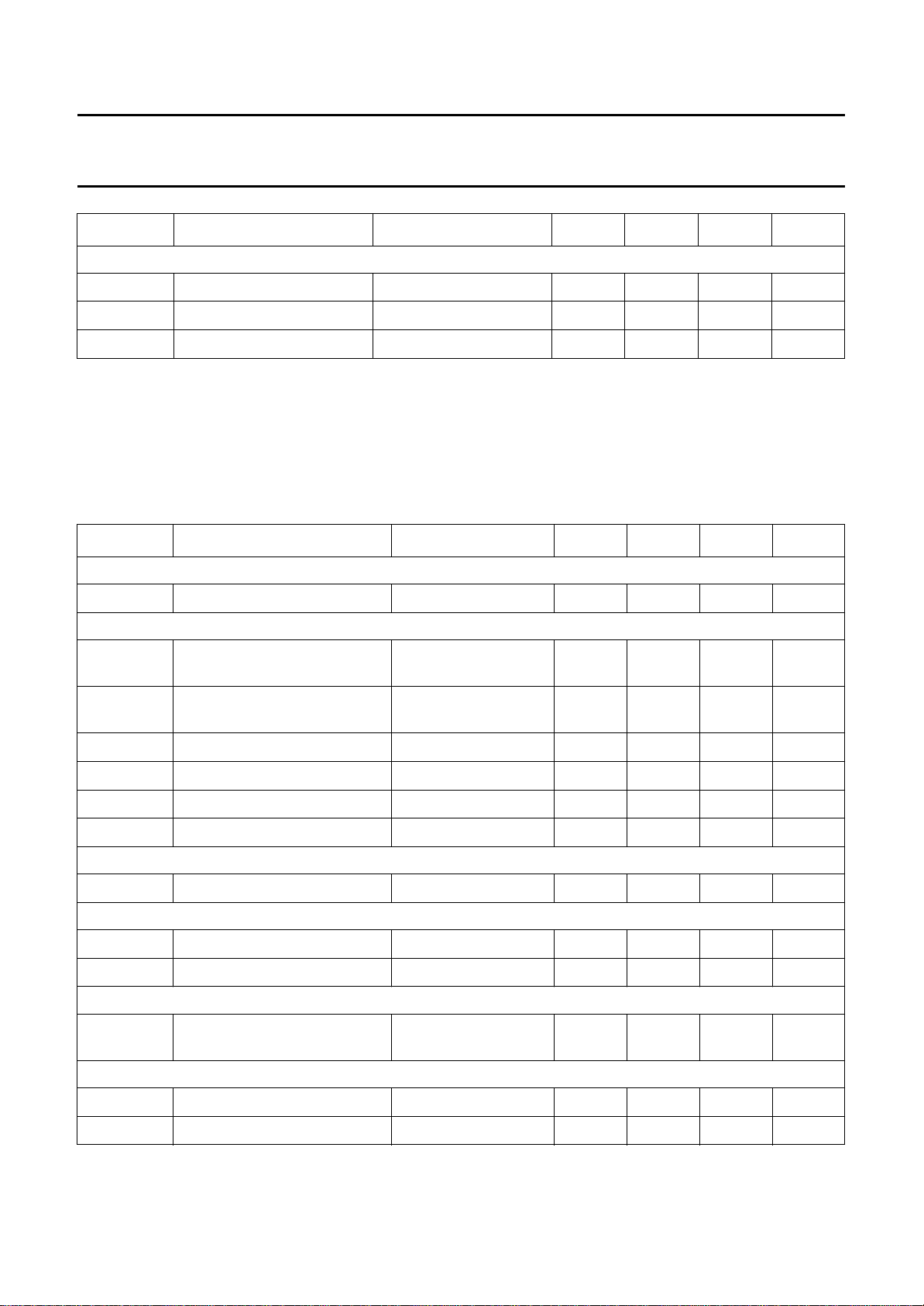
SYMBOL PARAMETER CONDITIONS MIN. TYP. MAX. UNIT
Output FS256 in 3-state
V
IL
V
IH
I
I
LOW level input voltage −−0.3V
HIGH level input voltage 0.7V
input current VI = VDD; T
= 25 °C40 − 250 µA
amb
−−V
DD
DD
V
Notes
1. For applications requiring minimum power dissipation the device may be operated from a nominal +4 V supply.
2. For load impedances representative of the application.
AC CHARACTERISTICS
VDD = 3.8 to 5.5 V; T
= −40 to +85 °C; unless otherwise specified.
amb
SYMBOL PARAMETER CONDITIONS MIN. TYP. MAX. UNIT
Inputs
C
I
input capacitance −−10 pF
X24IN and X22IN
f
xtal
crystal frequency at X22OUT,
note 1 21 22.5792 24 MHz
CLK22
f
xtal
crystal frequency at X24OUT,
note 1 23 24.576 26 MHz
CLK22
g
m
A
v
C
fb
C
O
mutual conductance f = 100 kHz 1.5 −−mA/V
small signal gain Av = gm.R
o
3.5 −−V/V
feedback capacitance −−5pF
output capacitance −−10 pF
Outputs
C
O
output capacitance −−10 pF
Inputs URDA, RESET, LTDATA, LTCLK, LTENSFC, LTNT0 and LTNT1
t
su
t
h
set-up time to X24IN 15 −−ns
hold time to X24IN 60 −−ns
Outputs LTDATA, MUTEDAC, DEEMDAC, ATTDAC, SYNCDAI, FDIR and FRESET
t
PD
propagation delay time from
−−80 ns
X24IN
Inputs FDAF, FDAC, SDA, SCL and SWS
t
su
t
h
set-up time to FS256 15 −−ns
hold time to FS256 25 −−ns
December 1993 32
Page 33
Philips Semiconductors Product specification
Stereo filter and codec SAA2002
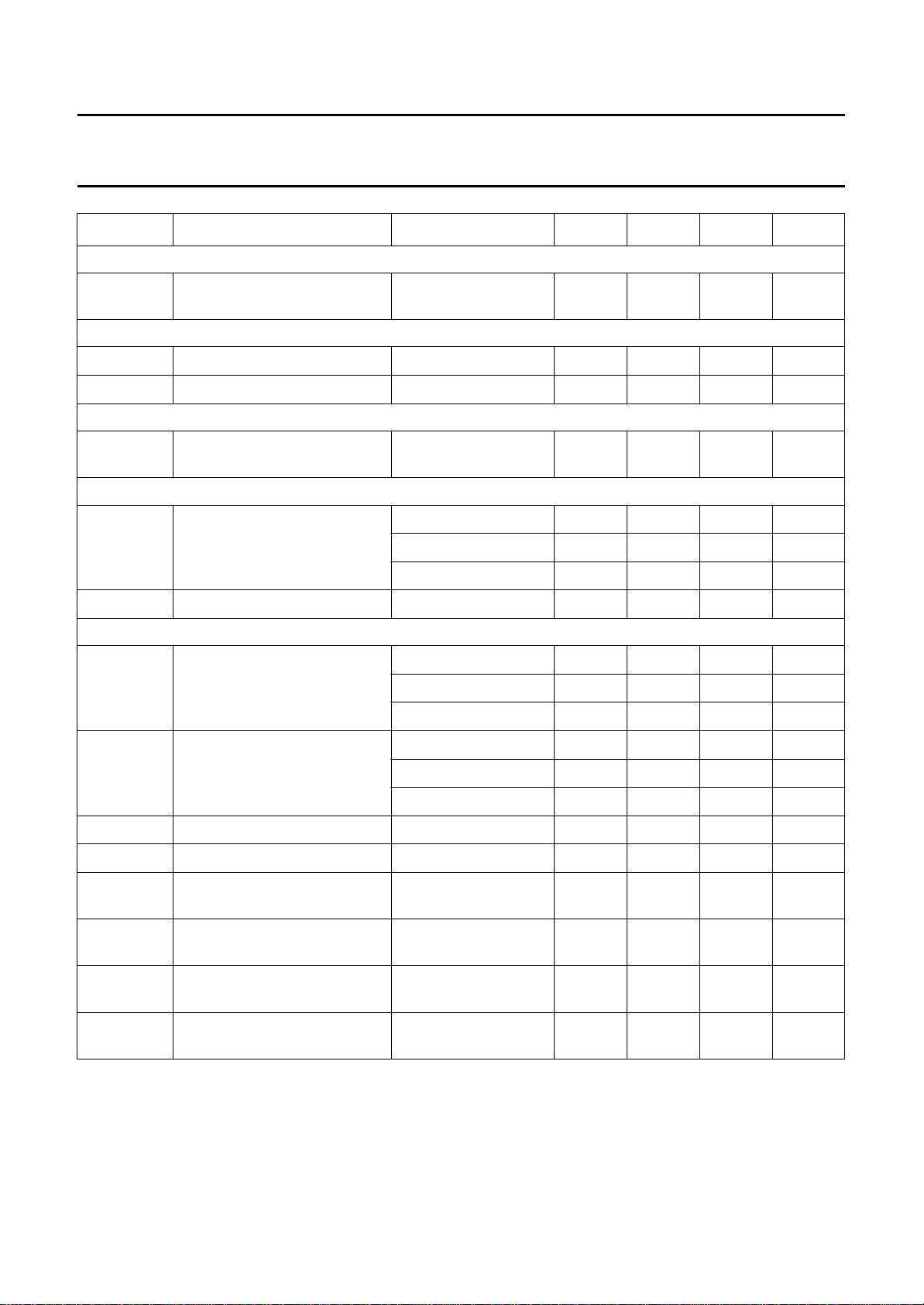
SYMBOL PARAMETER CONDITIONS MIN. TYP. MAX. UNIT
Outputs FDAF, FDAC, SDA, SCL, SWS and FSYNC
t
PD
propagation delay time from
FS256
Inputs SBDA, SBCL, SBWS, URDA, SBDIR and SBEF
t
su
t
h
set-up time to SBMCLK 15 −−ns
hold time to SBMCLK 25 −−ns
Outputs SBDA, SBCL and SBWS
t
PD
propagation delay time from
SBMCLK
FS256
T FS256 cycle time f
T
c
SCL cycle time − 4T − ns
= 48 kHz − 81.4 − ns
s
= 44.1 kHz − 88.6 − ns
f
s
f
= 32 kHz − 122.1 − ns
s
FS256 master mode (FS256, SCL and SWS are output)
t
fH
t
fL
t
sH
t
sL
t
su
FS256 HIGH time fs = 48 kHz 35 −−ns
= 44.1 kHz 38 −−ns
f
s
= 32 kHz 75 −−ns
f
s
FS256 LOW time fs = 48 kHz 35 −−ns
= 44.1 kHz 38 −−ns
f
s
= 32 kHz 75 −−ns
f
s
SCL HIGH time 2T − 20 −−ns
SCL LOW time 2T − 20 −−ns
SDA, FDAF, FDAC input set-up
time before FS256 HIGH
−−50 ns
−−50 ns
20 −−ns
t
h1
SDA, FDAF, FDAC input hold
time after FS256 HIGH
t
h2
SDA, FDAF, FDAC output hold
time after FS256 HIGH
t
d1,2
FS256 HIGH to SCL, SWS,
SDA, FDAF, FDAC output valid
December 1993 33
30 −−ns
0 −−ns
−−50 ns
Page 34
Philips Semiconductors Product specification
Stereo filter and codec SAA2002
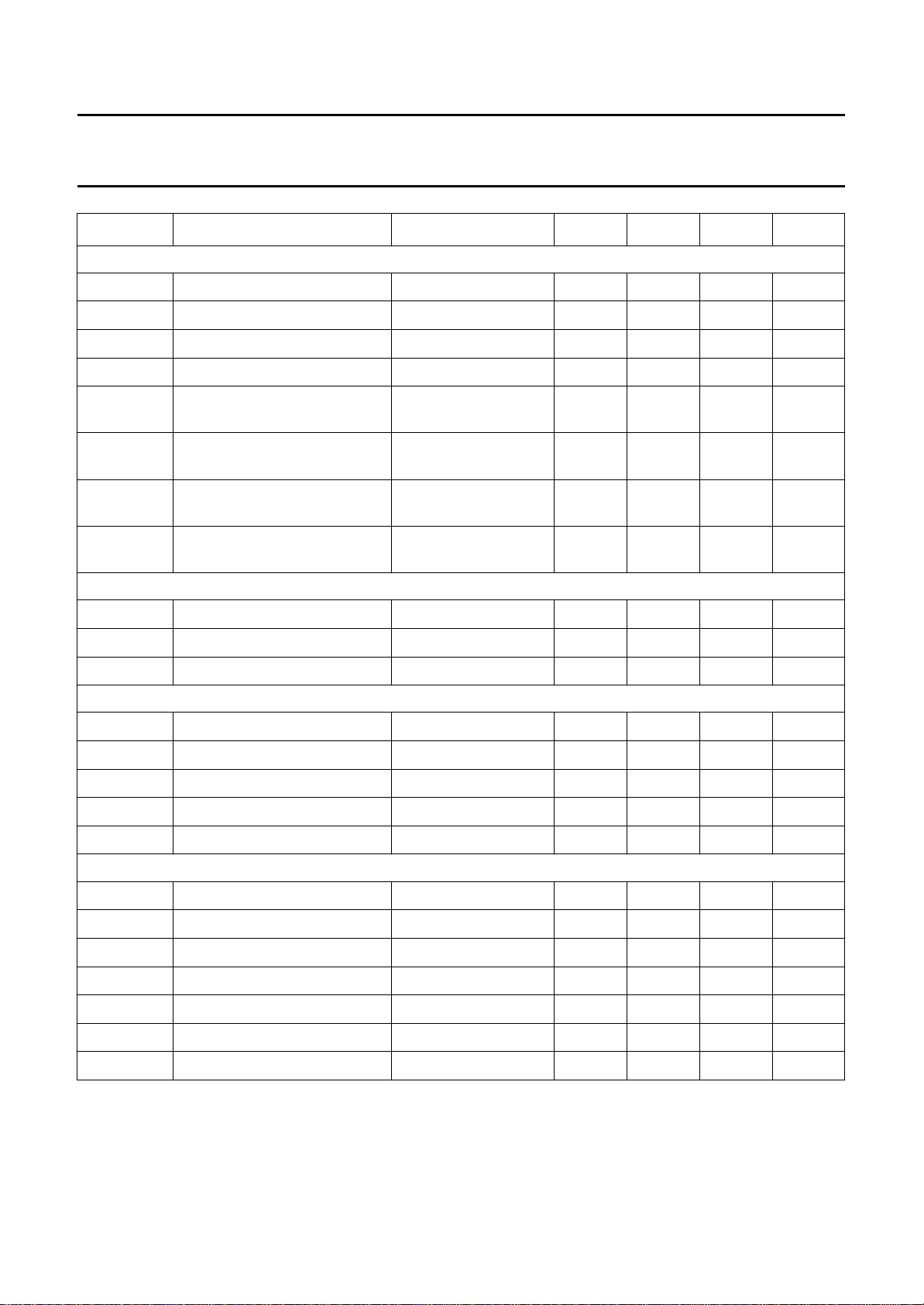
SYMBOL PARAMETER CONDITIONS MIN. TYP. MAX. UNIT
FS256 slave mode (FS256, SCL and SWS are input)
t
fH
t
fL
t
sH
t
sL
t
h1
FS256 HIGH time 35 −−ns
FS256 LOW time 35 −−ns
SCL HIGH time T + 35 −−ns
SCL LOW time T + 35 −−ns
SDA, FDAF, FDAC output hold
time after SCL HIGH
t
d
SCL HIGH to SDA, FDAF,
FDAC output valid
t
su
SDA, FDAF, FDAC input valid
after SCL HIGH
t
h2
SDA, FDAF, FDAC input hold
time after SCL HIGH
SBMCLK
T
s
t
mH
t
mL
SBMCLK cycle time 120 163 205 ns
SBMCLK HIGH time 35 −−ns
SBMCLK LOW time 75 −−ns
SBMCLK master mode (SBCL, SBWS and SBDA are output)
T
sc
t
cH
t
cL
t
d1
t
d2
SBCL cycle time 384 kbits/s − 8T
SBCL HIGH time 384 kbits/s 4Ts− 20 −−ns
SBCL LOW time 384 kbits/s 4Ts− 20 −−ns
SBWS, SBDA hold to SBCL LOW 20 −−ns
SBWS, SBDA valid after SBCL LOW −−20 ns
SBMCLK slave mode (SBCL, SBWS and SBDA are input)
2T − 15 −−ns
−−3T + 60 ns
20 −−ns
T + 20 −−ns
s
− ns
T
sc
t
cH
t
cL
t
su1
t
h1
t
su2
t
h2
SBCL cycle time − 8T
SBCL HIGH time Ts + 30 −−ns
SBCL LOW time Ts + 30 −−ns
SBWS, SBDA set-up time before SBCL HIGH Ts + 30 −−ns
SBWS, SBDA hold time after SBCL HIGH 30 −−ns
set-up time before SBEF valid after SBCL HIGH −−T
SBEF hold time after SBCL HIGH 2Ts− 30 −−ns
Notes
1. Percentage deviation from nominal frequency must be the same for X24, X22 and FS256 inputs within 0.2%.
2. For applications requiring minimum power dissipation the device may be operated from a nominal +4 V supply.
December 1993 34
s
− ns
− 30 ns
s
Page 35
Philips Semiconductors Product specification
Stereo filter and codec SAA2002
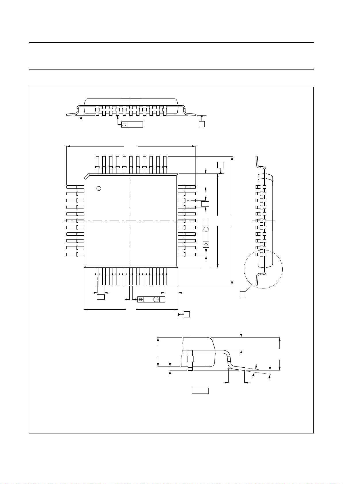
PACKAGE OUTLINE
seating plane
1
11
44
12
pin 1 index
1.0
0.50
0.35
0.15
19.2
18.2
14.1
13.9
S
0.15 M A
S
34
2.4
33
1.8
23
22
2.4
(4x)
1.8
A
1.0
0.50
0.35
(4x)
0.15 M B
14.1
13.9
B
19.2
18.2
X
Dimensions in mm.
December 1993 35
2.3
0.25
2.1
0.05
detail X
Fig.23 44-lead quad flat-pack; plastic (SOT205AG).
2.0
1.2
1.2
0.9
0.25
0.14
o
0 to 7
MBC659 - 1
2.60
2.15
Page 36
Philips Semiconductors Product specification
Stereo filter and codec SAA2002
SOLDERING
Quad flat-packs
YWAVE
B
During placement and before soldering, the component must
be fixed with a droplet of adhesive. After curing the adhesive,
the component can be soldered. The adhesive can be
applied by screen printing, pin transfer or syringe dispensing.
Maximum permissible solder temperature is 260 °C, and
maximum duration of package immersion in solder bath is
10 s, if allowed to cool to less than 150 °C within 6 s.
Typical dwell time is 4 s at 250 °C.
A modified wave soldering technique is recommended
using two waves (dual-wave), in which, in a turbulent wave
with high upward pressure is followed by a smooth laminar
wave. Using a mildly-activated flux eliminates the need for
removal of corrosive residues in most applications.
B
Y SOLDER PASTE REFLOW
Reflow soldering requires the solder paste (a suspension
of fine solder particles, flux and binding agent) to be
applied to the substrate by screen printing, stencilling or
pressure-syringe dispensing before device placement.
Several techniques exist for reflowing; for example,
thermal conduction by heated belt, infrared, and vapourphase reflow. Dwell times vary between 50 and 300 s
according to method. Typical reflow temperatures range
from 215 to 250 °C.
Preheating is necessary to dry the paste and evaporate
the binding agent. Preheating duration: 45 min at 45 °C.
EPAIRING SOLDERED JOINTS (BY HAND-HELD SOLDERING
R
IRON OR PULSE
-HEATED SOLDER TOOL)
Fix the component by first soldering two, diagonally
opposite, end pins. Apply the heating tool to the flat part of
the pin only. Contact time must be limited to 10 s at up to
300 °C. When using proper tools, all other pins can be
soldered in one operation within 2 to 5 s at between 270
and 320 °C. (Pulse-heated soldering is not recommended
for SO packages.)
For pulse-heated solder tool (resistance) soldering of VSO
packages, solder is applied to the substrate by dipping or
by an extra thick tin/lead plating before package placement.
DEFINITIONS
Data sheet status
Objective specification This data sheet contains target or goal specifications for product development.
Preliminary specification This data sheet contains preliminary data; supplementary data may be published later.
Product specification This data sheet contains final product specifications.
Limiting values
Limiting values given are in accordance with the Absolute Maximum Rating System (IEC 134). Stress above one or
more of the limiting values may cause permanent damage to the device. These are stress rating only and operation of
the device at these or at any other conditions above those given in the Characteristics sections of the specification is
not implied. Exposure to limiting values for extended periods may affect device reliability.
Application information
Where application information is given, it is advisory and does not form part of the specification.
LIFE SUPPORT APPLICATIONS
These products are not designed for use in life support appliances, devices, or systems where malfunction of these
products can reasonably be expected to result in personal injury. Philips customers using or selling these products for
use in such applications do so at their own risk and agree to fully indemnify Philips for any damages resulting from such
improper use or sale.
December 1993 36
Page 37

Philips Semiconductors Product specification
Stereo filter and codec SAA2002
The Digital Compact Cassette logo is a registered trade mark of Philips Electronics N.V.
December 1993 37
Page 38

Philips Semiconductors – a worldwide company
Argentina: IEROD, Av. Juramento 1992 - 14.b, (1428)
BUENOS AIRES, Tel. (541)786 7633, Fax. (541)786 9367
Australia: 34 Waterloo Road, NORTH RYDE, NSW 2113,
Tel. (02)805 4455, Fax. (02)805 4466
Austria: Triester Str. 64, A-1101 WIEN, P.O. Box 213,
Tel. (01)60 101-1236, Fax. (01)60 101-1211
Belgium: Postbus 90050, 5600 PB EINDHOVEN, The Netherlands,
Tel. (31)40 783 749, Fax. (31)40 788 399
Brazil: Rua do Rocio 220 - 5
CEP: 04552-903-SÃO PAULO-SP, Brazil.
P.O. Box 7383 (01064-970).
Tel. (011)829-1166, Fax. (011)829-1849
Canada: INTEGRATED CIRCUITS:
Tel. (800)234-7381, Fax. (708)296-8556
DISCRETE SEMICONDUCTORS: 601 Milner Ave,
SCARBOROUGH, ONTARIO, M1B 1M8,
Tel. (0416)292 5161 ext. 2336, Fax. (0416)292 4477
Chile: Av. Santa Maria 0760, SANTIAGO,
Tel. (02)773 816, Fax. (02)777 6730
Colombia: Carrera 21 No. 56-17, BOGOTA, D.E., P.O. Box 77621,
Tel. (571)217 4609, Fax. (01)217 4549
Denmark: Prags Boulevard 80, PB 1919, DK-2300 COPENHAGEN S,
Tel. (032)88 2636, Fax. (031)57 1949
Finland: Sinikalliontie 3, FIN-02630 ESPOO,
Tel. (9)0-50261, Fax. (9)0-520971
France: 4 rue du Port-aux-Vins, BP317,
92156 SURESNES Cedex,
Tel. (01)4099 6161, Fax. (01)4099 6427
Germany: P.O. Box 10 63 23, 20095 HAMBURG ,
Tel. (040)3296-0, Fax. (040)3296 213
Greece: No. 15, 25th March Street, GR 17778 TAVROS,
Tel. (01)4894 339/4894 911, Fax. (01)4814 240
Hong Kong: 15/F Philips Ind. Bldg., 24-28 Kung Yip St.,
KWAI CHUNG, Tel. (0)4245 121, Fax. (0)4806 960
India: PEICO ELECTRONICS & ELECTRICALS Ltd.,
Components Dept., Shivsagar Estate, Block 'A',
Dr. Annie Besant Rd., Worli, BOMBAY 400 018,
Tel. (022)4938 541, Fax. (022)4938 722
Indonesia: Philips House, Jalan H.R. Rasuna Said Kav. 3-4,
P.O. Box 4252, JAKARTA 12950,
Tel. (021)5201 122, Fax. (021)5205 189
Ireland: Newstead, Clonskeagh, DUBLIN 14,
Tel. (01)640 000, Fax. (01)640 200
Italy: Viale F. Testi, 327, 20162 MILANO,
Tel. (02)6752.1, Fax. (02)6752.3350
Japan: Philips Bldg13-37, Kohnan 2-chome, Minato-ku, KOKIO 108,
Tel. (03)3740 5101, Fax. (03)3740 0570
Korea: (Republic of) Philips House, 260-199 Itaewon-dong,
Yongsan-ku, SEOUL, Tel. (02)794-5011, Fax. (02)798-8022
Malaysia: No. 76 Jalan Universiti, 46200 PETALING JAYA,
SELANGOR, Tel. (03)757 5511, Fax. (03)757 4880
Mexico: Philips Components, 5900 Gateway East, Suite 200,
EL PASO, TX 79905, Tel. 9-5(800)234-7381, Fax. (708)296-8556
Netherlands: Postbus 90050, 5600 PB EINDHOVEN,
Tel. (040)78 37 49, Fax. (040)78 83 99
New Zealand: 2 Wagener Place, C.P.O. Box 1041, AUCKLAND,
Tel. (09)849-4160, Fax. (09)849-7811
Norway: Box 1, Manglerud 0612, OSLO,
Tel. (22)74 8000, Fax. (22)74 8341
th
floor, Suite 51,
Pakistan: Philips Markaz, M.A. Jinnah Rd., KARACHI 3,
Tel. (021)577 039, Fax. (021)569 1832
Philippines: PHILIPS SEMICONDUCTORS PHILIPPINES Inc,
106 Valero St. Salcedo Village, P.O. Box 911, MAKATI,
Metro MANILA, Tel. (02)810 0161, Fax. (02)817 3474
Portugal: Av. Eng. Duarte Pacheco 6, 1009 LISBOA Codex,
Tel. (01)683 121, Fax. (01)658 013
Singapore: Lorong 1, Toa Payoh, SINGAPORE 1231,
Tel. (65)350 2000, Fax. (65)251 6500
South Africa: 195-215 Main Road, Martindale,
P.O. Box 7430,JOHANNESBURG 2000,
Tel. (011)470-5433, Fax. (011)470-5494
Spain: Balmes 22, 08007 BARCELONA,
Tel. (03)301 6312, Fax. (03)301 42 43
Sweden: Kottbygatan 7, Akalla. S-164 85 STOCKHOLM,
Tel. (0)8-632 2000, Fax. (0)8-632 2745
Switzerland: Allmendstrasse 140, CH-8027 ZÜRICH,
Tel. (01)488 2211, Fax. (01)481 7730
Taiwan: 69, Min Sheng East Road, Sec 3, P.O. Box 22978,
TAIPEI 10446, Tel. (2)509 7666, Fax. (2)500 5899
Thailand: PHILIPS ELECTRONICS (THAILAND) Ltd.,
60/14 MOO 11, Bangna - Trad Road Km. 3
Prakanong, BANGKOK 10260,
Tel. (2)399-3280 to 9, (2)398-2083, Fax. (2)398-2080
Turkey: Talatpasa Cad. No. 5, 80640 LEVENT/ISTANBUL,
Tel. (0212)279 2770, Fax. (0212)269 3094
United Kingdom: Philips Semiconductors Limited, P.O. Box 65,
Philips House, Torrington Place, LONDON, WC1E 7HD,
Tel. (071)436 41 44, Fax. (071)323 03 42
United States:INTEGRATED CIRCUITS:
811 East Arques Avenue, SUNNYVALE, CA 94088-3409,
Tel. (800)234-7381, Fax. (708)296-8556
DISCRETE SEMICONDUCTORS: 2001 West Blue Heron Blvd.,
P.O. Box 10330, RIVIERA BEACH, FLORIDA 33404,
Tel. (800)447-3762 and (407)881-3200, Fax. (407)881-3300
Uruguay: Coronel Mora 433, MONTEVIDEO,
Tel. (02)70-4044, Fax. (02)92 0601
For all other countries apply to: Philips Semiconductors,
International Marketing and Sales, Building BAF-1,
P.O. Box 218, 5600 MD, EINDHOVEN, The Netherlands,
Telex 35000 phtcnl, Fax. +31-40-724825
SCD27 © Philips Electronics N.V. 1993
All rights are reserved. Reproduction in whole or in part is prohibited without the
prior written consent of the copyright owner.
The information presented in this document does not form part of any quotation
or contract, is believed to be accurate and reliable and may be changed without
notice. No liability will be accepted by the publisher for any consequence of its
use. Publication thereof does not convey nor imply any license under patent- or
other industrial or intellectual property rights.
Printed in The Netherlands
Philips Semiconductors
 Loading...