

Page 1
sames
THREE PHASE POWER/ENERGY METERING
IC WITH INSTANTANEOUS PULSE OUTPUT
FEATURES
n Functionally similar to the SA9105E
and SA9105F, with reduced number of
external components
n Output frequency represents the abso-
lute sum of energy on all three phases
n Performs one, two or three phase power
and energy measurement
n Meets the IEC 521/1036 Specification
requirements for Class 1 AC Watt hour
meters
SA9605A
n Operates over a wide temperature
range
n Current transformers for sensing
n Excellent long term stability
n Easily adaptable to different signal
levels
n Precision voltage reference on-chip
n Pin selectable pulse rates
n Supports tamper detection
DESCRIPTION
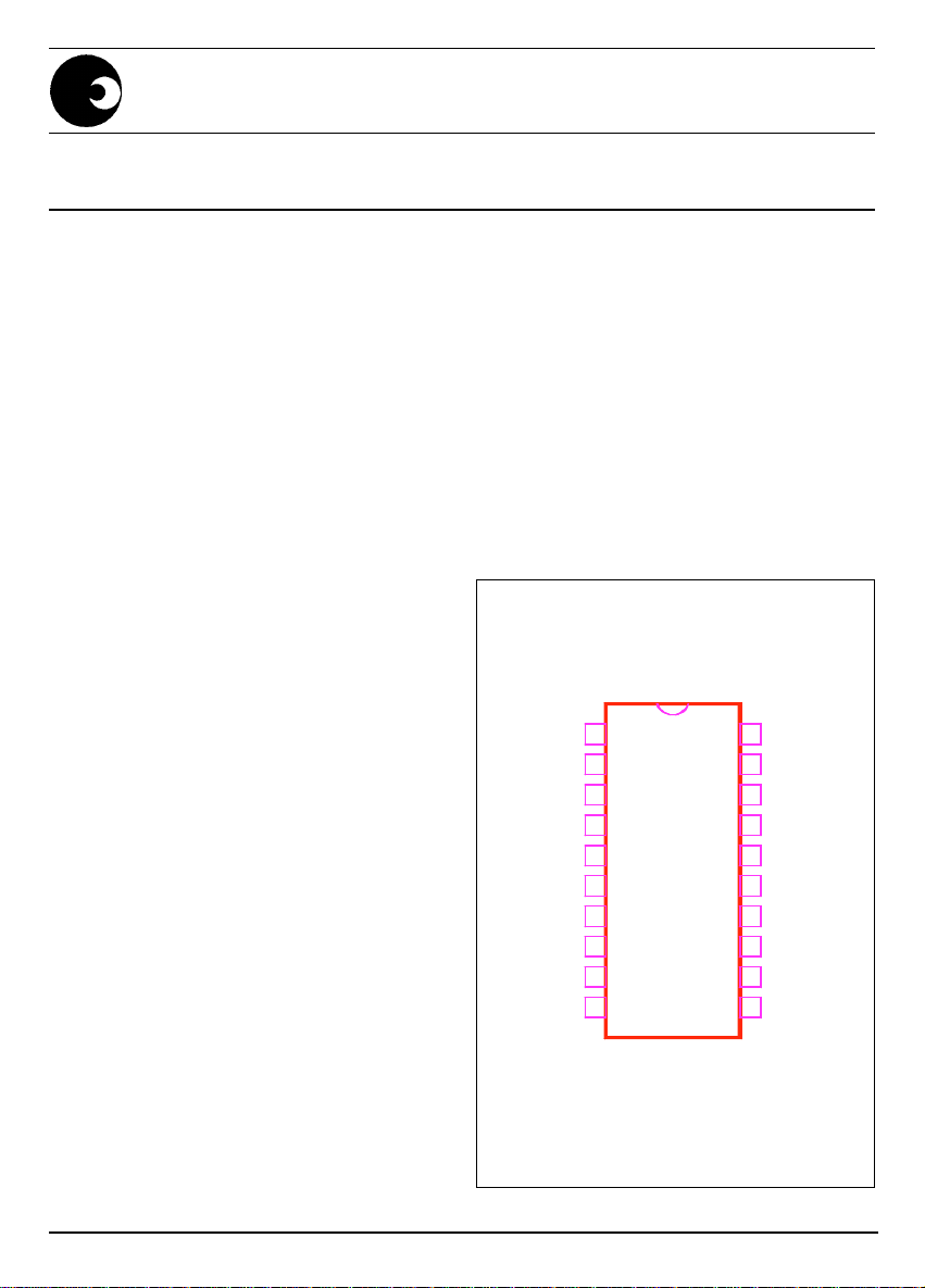
PIN CONNECTIONS
The SAMES SA9605A is an enhancement
of the SA9105E and SA9105F, as no external
capacitors are needed for the A/D converters.
The SAMES SA9605A Three Phase Power/
Energy metering integrated circuit generates
a pulse rate output, the frequency of which
is proportional to the absolute power consumption. The SA9605A performs the
calculation for active power.
The method of calculation takes the power
factor into account.
Energy consumption is determined by the
power measurement being integrated over
time.
The output of this innovative universal three
phase power/energy metering integrated
circuit, is ideally suited for applications such
as residential and industrial energy metering
IIP2
IIN2
IVN3
IIP3
IIN3
V
FOUT1
FOUT2
DIR
OSC1
DD
1
2
3
4
5
6
7
8
9
10
DR-01109
20
19
18
17
16
15
14
13
12
11
IVP2
IIN1
IIP1
IVN1
GND
VREF
V
SS
PGM1
PGM0
OSC2
and control.
The SA9605A integrated circuit is available
in both 20-pin dual-in-line plastic (DIP-20),
as well as 20-pin plastic small outline (SOIC-
Package: DIP-20
SOIC-20
20) package types.
4452 PDS039-SA9605A-001 Rev. B 14-03-97
1/14
Page 2
SA9605A
BLOCK DIAGRAM
TO
RATE
V
OSC
DD
V
SS
FOUT1
FOUT2
DIR
OSC1
OSC2
IVN1
IVN2
IVN3
IIP1
IIN1
IIP2
IIN2
IIP3
IIN3
GND
VREF
DR-01110
ANALOG
SIGNAL
PRO-
CESSING
REF
PGM1
PGM0
POWER
INTEG.
&
PULSE
AVERAGE
TIMING & CONTROL
ABSOLUTE MAXIMUM RATINGS *
Parameter Symbol Min Max Unit
Supply Voltage VDD-V
Current on any Pin I
Storage Temperature T
Operating Temperature T
Current at any pin I
PIN
STG
O
P
SS
-0.3 6.0 V
-150 +150 mA
-40 +125 °C
-40 +85 °C
-100 +100 mA
* Stresses above those listed under "Absolute Maximum Ratings" may cause permanent
damage to the device. This is a stress rating only. Functional operation of the device
at these or any other conditions above those indicated in the operation sections of this
specification, is not implied. Exposure to Absolute Maximum Ratings for extended
periods may affect device reliability.
2/14
sames
Page 3

SA9605A
ELECTRICAL CHARACTERISTICS
(VDD = 2.5V, VSS = -2.5V, over the temperature range -10°C to +70°C#, unless otherwise
specified.)
Parameter Symbol Min Typ Max Unit Condition
Operating Temperature
Range
Supply Voltage VDD-V
Supply Current I
#
T
O
DD
-25 +85 °C
4.5 5.5 V
SS
15 mA
Nonlinearity of
Power Calculation -0.3 +0.3 % 1% - 100% of
rated power
Current Sensor Inputs (Differential)
Input Current Range I
II
-25 +25 µA Peak value
Voltage Sensor Inputs (Asymmetric)
Input Current Range I
IV
-25 +25 µA Peak value
Pins FOUT1, FOUT2, DIR
Output Low Voltage V
Output High Voltage V
Pulse Rate: FOUT1 f
OL
OH
p
VDD-1 V IOH = -2mA
10 1160 Hz Specified linearity
VSS+1 V IOL = 5mA
3000 Hz Min and max limits
FOUT2 User selectable
Oscillator Recommended crystal:
TV colour burst crystal, f = 3.5795 MHz
Pin VREF With R = 24 kΩ
Ref. Current -I
Ref. Voltage V
#
Extended Operating Temperature Range available on request.
R
R
45 50 55 µA connected to V
1.1 1.3 V Referred to V
sames
SS
SS
3/14
Page 4

SA9605A
PIN DESCRIPTION
Pin
Designation Description
16 GND Ground
6VDDPositive Supply Voltage
14 V
SS
Negative Suply Voltage
17 IVN1 Analog input for Voltage : Phase 1
20 IVN2 Analog input for Voltage : Phase 2
3 IVN3 Analog input for Voltage : Phase 3
19 IIN1 Inputs for Current sensor : Phase 1
18 IIP1
2 IIN2 Inputs for Current sensor : Phase 2
1 IIP2
5 IIN3 Inputs for Current sensor : Phase 3
4 IIP3
10 OSC1 Connections for crystal or ceramic resonator
11 OSC2 (OSC1 = Input ; OSC2 = Output)
7 FOUT1 Pulse rate outputs
8 FOUT2
9 DIR Direction indicator
12 PGM0 FOUT2 Frequency select pins
13 PGM1
15 VREF Connection for current setting resistor
FUNCTIONAL DESCRIPTION
The SAMES SA9605A is a CMOS mixed signal Analog/Digital integrated circuit, which
performs three phase power/energy calculations over a range of 1000:1, to an overall
accuracy of better than Class 1.
The SA9605A in both DIP-20 and SOIC-20 package options is functionally similar to the
SA9105E and SA9105F with the advantage of no external loop capacitors.
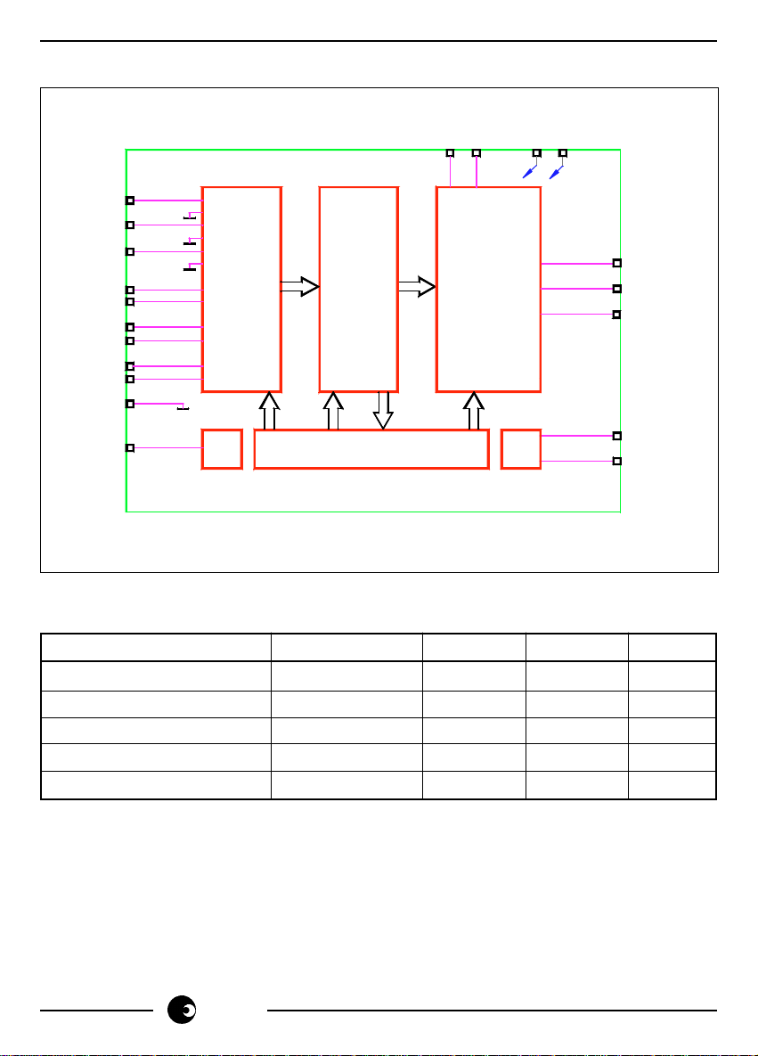
The integrated circuit includes all the required functions for 3-phase power and energy
measurement such as oversampling A/D converters for the voltage and current sense
inputs, power calculation and energy integration. Internal offsets are eliminated through
the use of cancellation procedures.
The SA9605A generates pulses, the frequency of which is proportional to the power
consumption. Two frequency outputs (FOUT1 and FOUT2) are available. The pulse rate
follows the instantaneous power measured.
4/14
sames
Page 5

1. Power Calculation
In the Application Circuit (Figure 1), the mains voltages from Line 1, Line 2 and Line
3, are converted to currents and applied to the voltage sense inputs IVN1, IVN2 and
IVN3.
The current levels on the voltage sense inputs are derived from the mains voltage
(3 x 230 VAC) being divided down through voltage dividers to 14V. The resulting
input currents into the A/D converters are 14µA through the resistors R15, R16 and
R17.
For the current sense inputs the voltage drop across the current transformers
terminating resistors are converted to currents of 16µA for rated conditions, by
means of resistors R8, R9 (Phase 1); R10, R11 (Phase 2); and R12, R13 (Phase 3).
The signals providing the current information are applied to the current sensor
inputs: IIN1, IIP1; IIN2, IIP2; and IIN3, IIP3.
In this configuration, with the mains voltage of 3 x 230 V and rated currents of 80A,
the output frequency of the SA9605A energy metering integrated circuit at FOUT1
is 1.16kHz. In this case 1 pulse will correspond to an energy consumption of 3 x 18.4
kW/1160Hz = 47.6 Ws.
The output frequency at FOUT1 and FOUT2 represents the absolute sum of the
energy measured on all three phases, regardless of the direction of energy flow
through the current sensors. This measurement method will assist meter
manufacturers to circumvent meter tampering by reversal of the phases.
SA9605A
2. Analog Input Configuration
The current and voltage sensor inputs are illustrated below.
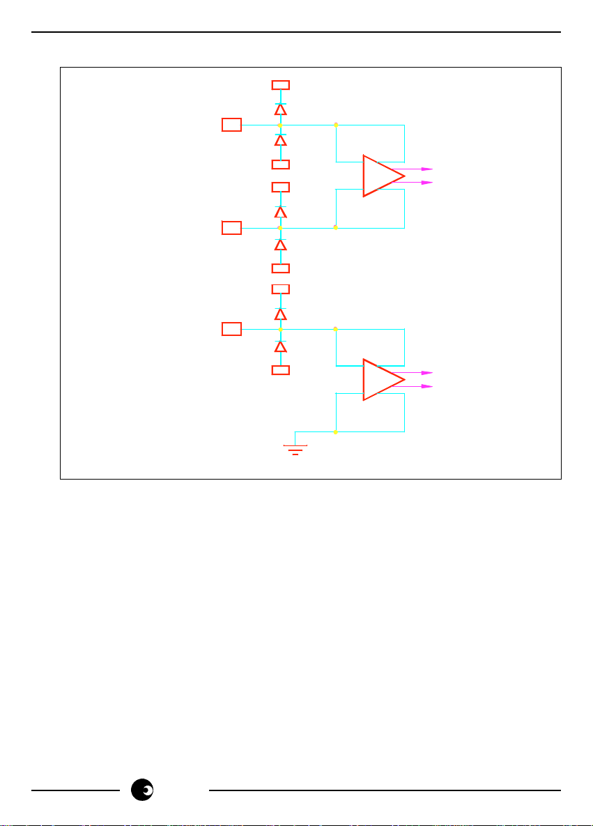
These inputs are protected against electrostatic discharge through clamping
diodes, in conjunction with the amplifiers input configuration.
The feedback loops from the outputs of the amplifiers AI and AV generate virtual
shorts on the signal inputs. Exact duplications of the input currents are generated
for the analog processing circuitry.
sames
5/14
Page 6
SA9605A
CURRENT
SENSOR
INPUTS
IVN
IIP
IIN
V
DD
V
SS
A
V
DD
V
SS
V
DD
I
VOLTAGE
SENSOR
INPUT
DR-01111
V
SS
GND
A
V
3. Electrostatic Discharge (ESD) Protection
The SA9605A integrated circuit's inputs/outputs are protected against ESD.
4. Power Consumption
The overall power consumption rating of the SA9605A integrated circuit is less than
75mW with a 5V supply.
5. Pulse Output Signals
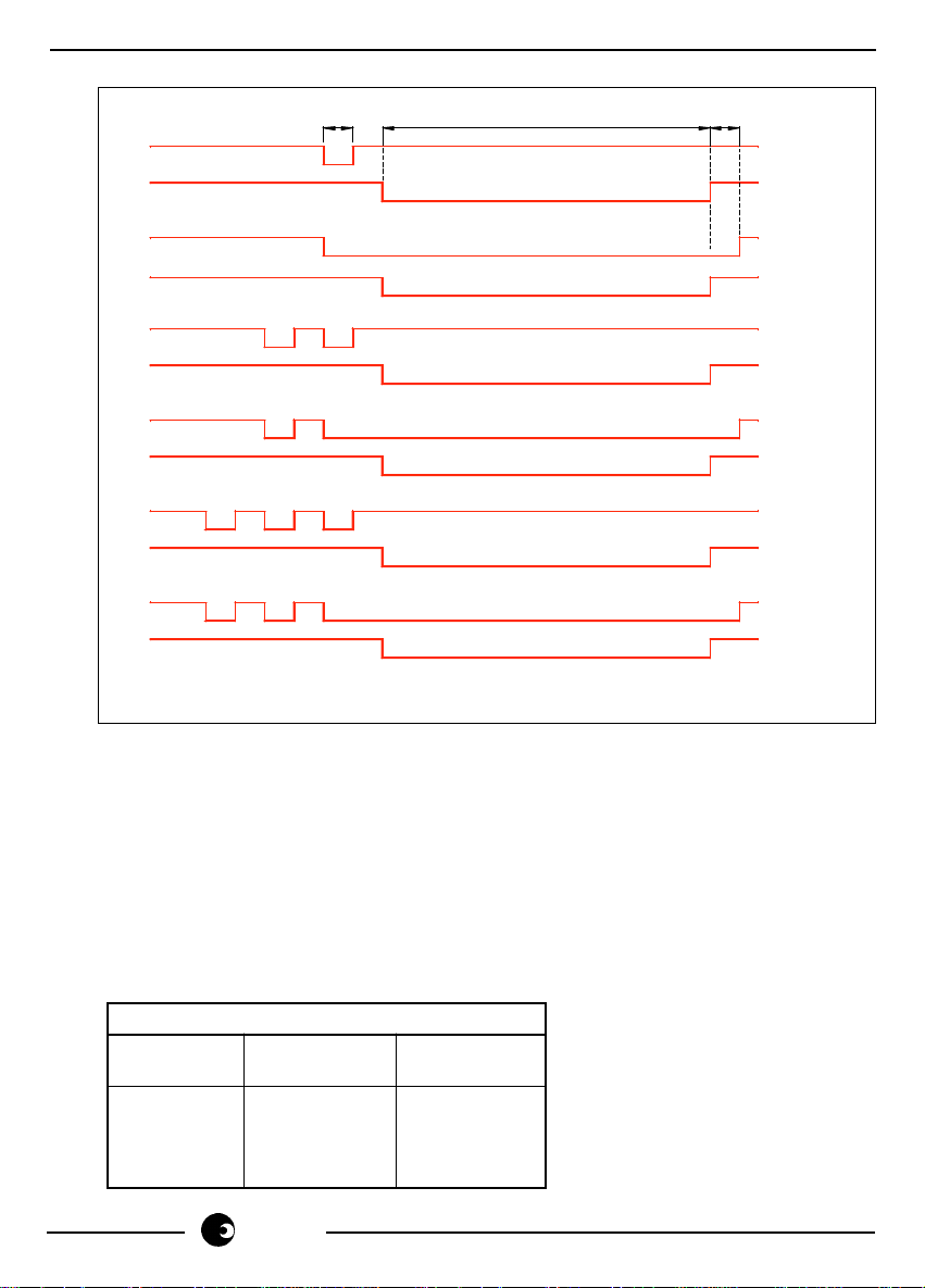
Waveforms displaying the DIR and FOUT1 signal information for each of the
three phases are shown below.
6/14
sames
Page 7
SA9605A
DIR
FOUT1
DIR
FOUT1
DIR
FOUT1
DIR
FOUT1
DIR
FOUT1
DIR
FOUT1
DR-01145
8.94 s
µµ
71.55 s
µµ
8.94 s
µµ
PHASE 1,
POSITIVE
PHASE 1,
NEGATIVE
PHASE 2,
POSITIVE
PHASE 2,
NEGATIVE
PHASE 3,
POSITIVE
PHASE 3,
NEGATIVE
These waveforms demonstrate how to establish the direction of energy flow as well
as the phase from which the energy is measured. The direction of energy indicated
on pin DIR is HIGH for POSITIVE energy flow and LOW for NEGATIVE energy flow,
for the entire LOW period of the FOUT1 pulse. The phase to which the direction
indication on the DIR pin refers can be ascertained by counting the number of falling
edges on the DIR pin prior to the falling edge of the FOUT1 pulse. The supervision
of the DIR pin can be accomplished with a µController.
Although FOUT1 has a fixed frequency output, the table below shows the various
frequencies selectable for rated conditions on FOUT2.
User Selectable Output Frequency
PGM1 PGM0
FOUT2
(Hz)
0 0 5.11
0 1 3.83
1 0 2.55
1 1 N/A
sames
7/14
Page 8

SA9605A
The frequencies shown in the above table were chosen to allow a 4 - 3 - 2 scaling ratio
for rated conditions. This facility provides ease of interface with applications which use
the same post divider with mechanical counter or unchanged microcontroller software
for different current rated kWh meters.
For example, a meter manufacturer may wish to build meters for 3 system configurations
with rated current loading of 80A
230V
RMS
.
RMS
, 60A
and 40A
RMS
. The rated line voltage is
RMS
FOUT1 Frequency
Consider the case where FOUT1 is the output of the energy counting block. For each
of the three rated conditions, the input current sensing resistors are chosen to ensure that
16µA
Case 1 IL = 80A
Case 2 IL = 60A
Case 3 IL = 40A
flows into the current sensing pins.
RMS
RMS
1 pulse on FOUT1 =
RMS
1 pulse on FOUT1 =
RMS
1 pulse on FOUT1 =
80 * 230 * 3
1160
60 * 230 * 3
1160
40 * 230 * 3
1160
= 47.6Ws
= 35.7Ws
= 23.8Ws
The amount of energy represented by one pulse for each of the three cases is different.
In addition to changing the current sensing resistor network, the energy counting block
must also be altered.
FOUT2 Frequency
Now consider the advantage of the user selectable frequency available on FOUT2.
Again the input current sensing resistors must be chosen to ensure that 16µA
RMS
flows
into the current sensing pins.
Case 1 IL = 80A
1 pulse on FOUT2 =
Case 2 IL = 60A
1 pulse on FOUT2 =
Case 3 IL = 40A
1 pulse on FOUT2 =
8/14
, PGM1 = 0 PGM0 = 0
RMS
, PGM1 = 0 PGM0 = 1
RMS
PGM1 = 1 PGM0 = 0
RMS,
80 * 230 * 3
5.11
60 * 230 * 3
3.83
40 * 230 * 3
2.55
= 10.8kWs
= 10.8kWs
= 10.8kWs
sames
Page 9

SA9605A
The only changes which now have to be implemented to interface the device to different
rated systems are: change the current sense resistors; and select the required PGM0
and PGM1.
No change to the post divider or micro-controller software is required if the FOUT2 pin
is used as described.
TYPICAL APPLICATION
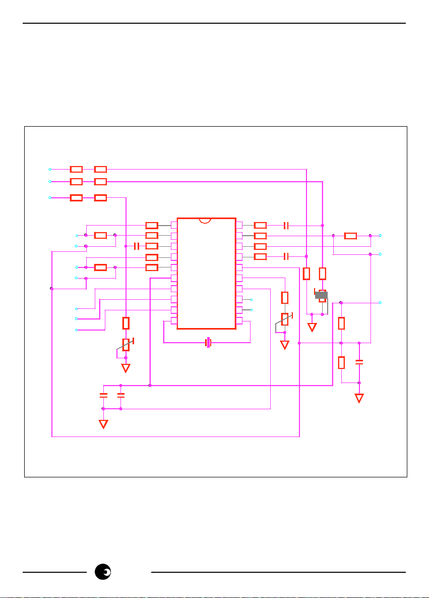
In the Application Circuit (Figure 1), the components required for a three phase power
metering application are shown.
Terminated current sensors (current transformers) are connected to the current sensor
inputs of the SA9605A through current setting resistors (R8 ..R13).
The resistor values for standard operation are selected for an input current of 16µA into
the SA9605A, at the rated line current.
The values of these resistors are calculated as follows:
Phase 1:
R8 = R9 = (IL1/16µA) * R18/2
Phase 2:
R10 = R11 = (IL2/16µA) * R19/2
Phase 3:
R12 = R13 = (IL3/16µA) * R20/2
Where I
LX
R18, R19 and R
= Secondary CT current at rated conditions.
= Current transformer termination resistors for the three phases.
20
R1 + R1A, R4 and R15 set the current for the phase 1 voltage sense input. R2 + R2A, R5 +
P5 and R16 set the current for phase 2 and R3 + R3A, R6 + P6 and R17 set the current for phase
3. The values should be selected so that the input currents into the voltage sense inputs
(virtual ground) are set to 14µA for rated line voltage. Capacitors C1, C2 and C3 are for
decoupling and phase compensation.
R
+ P14 defines all on-chip bias and reference currents. With R14+ P14 = 24kΩ, optimum
14
conditions are set. R
changes to R
+ P14 will affect the output quadratically (i.e: ∆R = +5%, ∆f = +10%).
14
+ P14 may be varied within ± 10% for calibration purposes. Any
14
The formula for calculating the Output Frequency (f) is given below:
f = 11.16
3.5795MHz 3 * I
FOUTX
*
FOSC * (II1 IV1) + (II2 IV2) + (II3 IV3)
*
2
R
Where FOUTX = Nominal rated frequency (1160Hz)
FOSC = Oscillator frequency (2MHz ...... 4MHz)
II1, II2, II3= Input currents for current inputs (16µA at rated)
IV1, IV2, IV3= Input currents for voltage inputs (14µA at rated)
I
R
= Reference current (typically 50µA)
sames
9/14
Page 10
SA9605A
XTAL is a colour burst TV crystal (f = 3.5795 MHz) for the oscillator. The oscillator
frequency is divided down to 1.78975 MHz on-chip, to supply the digital circuitry and the
A/D converters.
Figure 1: Application Circuit for Three Phase Power/Energy Measurement.
MAINS VOLTAGES
R1
LINE 1
LINE 2
LINE 3
R2
R3
R1A
R2A
R3A
DR-01112
VI2P
VI2N
VI3P
VI3N
FOUT1
FOUT2
DIR
C13
0V
R19
R20
R6
P6
C12
PGM1
PGM0
R16
R8
R9
R15
C2
C1
R14
P14
0V
R18
R5R4
P5
R7
0V
R21
VI1P
VI1N
5V
C14
0V
R11
1
R10
R17
R13
R12
2
3
4
5
6
7
8
9
10
SA9605A
DIP - 20
IC-1
C3
0V
20
19
18
17
16
15
14
13
12
11
XTAL
10/14
sames
Page 11

Parts List for Application Circuit: Figure 1
Item Symbol Description Detail
1 IC-1 Integrated SA9605A DIP-20, SOIC-20
2 XTAL Crystal, 3.5795 MHz Colour burst TV
3 R1 Resistor, 200k, 1%, ¼W
4 R1A Resistor, 180k, 1%, ¼W
5 R2 Resistor, 200k, 1%, ¼W
6 R2A Resistor, 200k, 1%, ¼W
7 R3 Resistor, 200k, 1% , ¼W
8 R3A Resistor, 180k, 1%, ¼W
9 R4 Resistor, 24k, 1%, ¼W
10 R5 Resistor, 22k, 1%, ¼W
11 R6 Resistor, 22k, 1%, ¼W
12 R7 Resistor, 820Ω, 1%, ¼W
13 R8 Resistor Note 1
14 R9 Resistor Note 1
15 R10 Resistor Note 1
16 R11 Resistor Note 1
17 R12 Resistor Note 1
18 R13 Resistor Note 1
19 R14 Resistor, 22k, 1%, ¼W
20 R15 Resistor, 1M, 1%, ¼W
21 R16 Resistor, 1M, 1%, ¼W
22 R17 Resistor, 1M, 1%, ¼W
23 R18 Resistor Note 1
24 R19 Resistor Note 1
25 R20 Resistor Note 1
26 R21 Resistor, 820Ω, 1%, ¼W
27 P5 Potentiometer, 4.7k Multi turn
28 P6 Potentiometer, 4.7k Multi turn
29 P14 Potentiometer, 4.7k Multi turn
30 C1 Capacitor, electrolytic, 1µF, 6V Note 2
31 C2 Capacitor, electrolytic, 1µF, 6V Note 2
32 C3 Capacitor, electrolytic, 1µF, 6V Note 2
33 C12 Capacitor, 820nF Note 3
34 C13 Capacitor, 100nF
35 C14 Capacitor, 100nF
SA9605A
sames
11/14
Page 12

SA9605A
Note 1: Resistor (R8, R9, R10, R11, R12 and R13) values are dependant upon the selected
values of the current transformer termination resistors R18, R19 and R20.
Note 2: Capacitor values may be selected to compensate for phase errors caused by
the current transformers.
Note 3: Capacitor (C12) to be positioned as close to Supply Pins (VDD & V
as possible.
ORDERING INFORMATION
Part Number Package
SA9605APA DIP-20
SA9605ASA SOIC-20
) of IC-1,
SS
12/14
sames
Page 13

NOTES:
SA9605A
sames
13/14
Page 14

SA9605A
Disclaimer: The information contained in this document is confidential and proprietary to South African Micro-
Electronic Systems (Pty) Ltd ("SAMES") and may not be copied or disclosed to a third party, in whole or in part,
without the express written consent of SAMES. The information contained herein is current as of the date of
publication; however, delivery of this document shall not under any circumstances create any implication that the
information contained herein is correct as of any time subsequent to such date. SAMES does not undertake to inform
any recipient of this document of any changes in the information contained herein, and SAMES expressly reserves
the right to make changes in such information, without notification,even if such changes would render information
contained herein inaccurate or incomplete. SAMES makes no representation or warranty that any circuit designed
by reference to the information contained herein, will function without errors and as intended by the designer.
Any Sales or technical questions may be posted to our e-mail address below:
[email protected]
For the latest updates on datasheets, please visit our web site:
http://www.sames.co.za
South African Micro-Electronic Systems (Pty) Ltd
P O Box 15888, 33 Eland Street,
Lynn East, Koedoespoort Industrial Area,
0039 Pretoria,
Republic of South Africa, Republic of South Africa
Tel: 012 333-6021 Tel: Int +27 12 333-6021
Fax: 012 333-8071 Fax: Int +27 12 333-8071
14/14
sames
 Loading...