

Page 1
sames
SA9602H
SINGLE PHASE BIDIRECTIONAL POWER/ENERGY
METERING IC WITH INSTANTANEOUS PULSE OUTPUT
FEATURES
■ Performs bidirectional power and
energy measurement
■ Meets the IEC 521/1036 Specification
requirements for Class 1 AC Watt hour
meters
■ Protected against ESD
■ Total power consumption rating below
25mW
■ Adaptable to different types of current
sensors
■ Operates over a wide temperature range
■ Precision voltage reference on-chip
DESCRIPTION
The SAMES SA9602H is an enhancement of
the SA9102H, as no external capacitors are
required for the A/D converters. The SA9602H
has a higher output pulse rate than the
SA9102H.
The SAMES SA9602H Single Phase
bidirectional Power/Energy metering integrated
circuit generates a pulse rate output, the
frequency of which is proportional to the power
consumption. The SA9602H performs the
calculation for active power.
The method of calculation takes the power
factor into account.
Energy consumption can be determined by
the power measurement being integrated over
time.
This innovative universal single phase power/
energy metering integrated circuit is ideally
suited for energy calculations in applications
such as residential municipal metering and
factory energy metering and control.
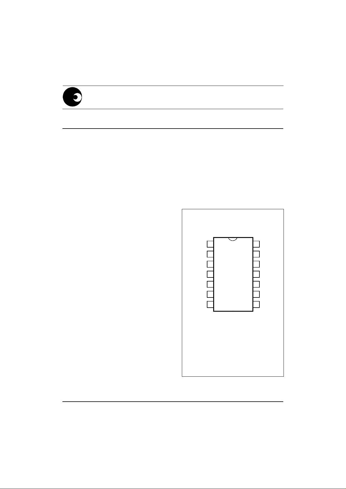
The SA9602H integrated circuit is available in
both 14 and 20 pin dual-in-line plastic (DIP-14/
DIP-20), as well as 20 pin small outline (SOIC-
20) package types.
PIN CONNECTIONS
IIN
IIP
VREF
TEST
V
OSC2
OSC1
DD
1
2
3
4
5
6
7
DR-01276
Package: DIP-14
14
13
12
11
10
9
8
GND
IVP
TP12
FMO
V
SS
DIR
FOUT
7149 PDS039-SA9602H-001 REV.D 27-08-98
1/14
Page 2
SA9602H
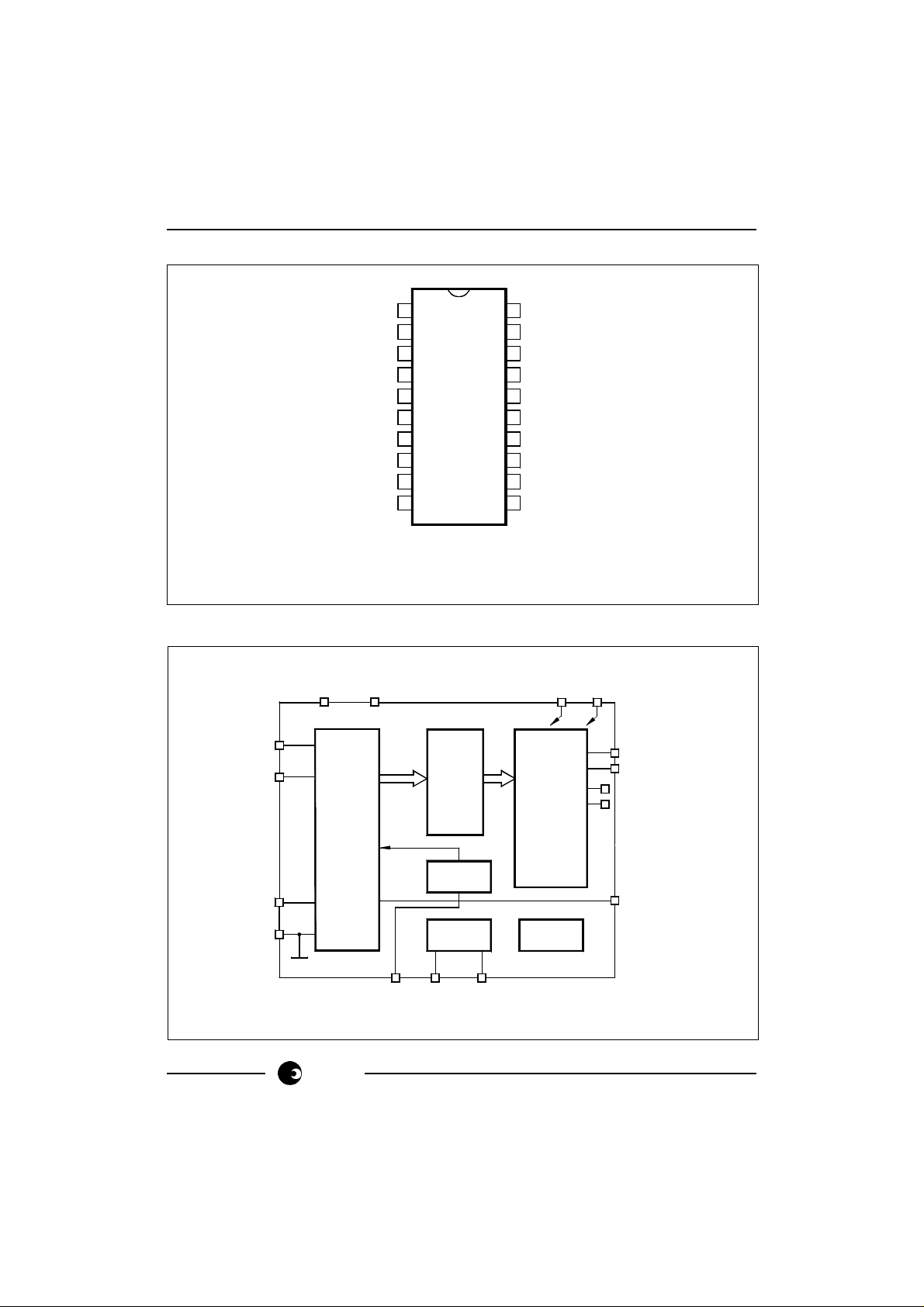
PIN CONNECTIONS
BLOCK DIAGRAM
IIP
IIN
TE S T
ANALOG
SIGNAL
1
IIN
2
IIP
VREF
3
4
TP4
5
TP5
6
TP6
7
TEST
V
8
DD
9
TP9
10
OSC2
D R-01277
Package: DIP-20
TEST2
POWER
INTEGRATOR
SOIC-20
GND
20
19
IVP
18
TP17
17
TEST2
16
TP16
15
FMO
V
14
SS
13
DIR
12
FOUT
11
OSC1
POWER
FREQUENCY
TO
VV
SSDD
FOU T
DIR
2/14
IV P
GND
DR -01278
sames
PROCE-
SSING
VOLTAGE
VREF OS C 1
REF.
OSC
FMO
TIMING
OS C 2
Page 3
SA9602H
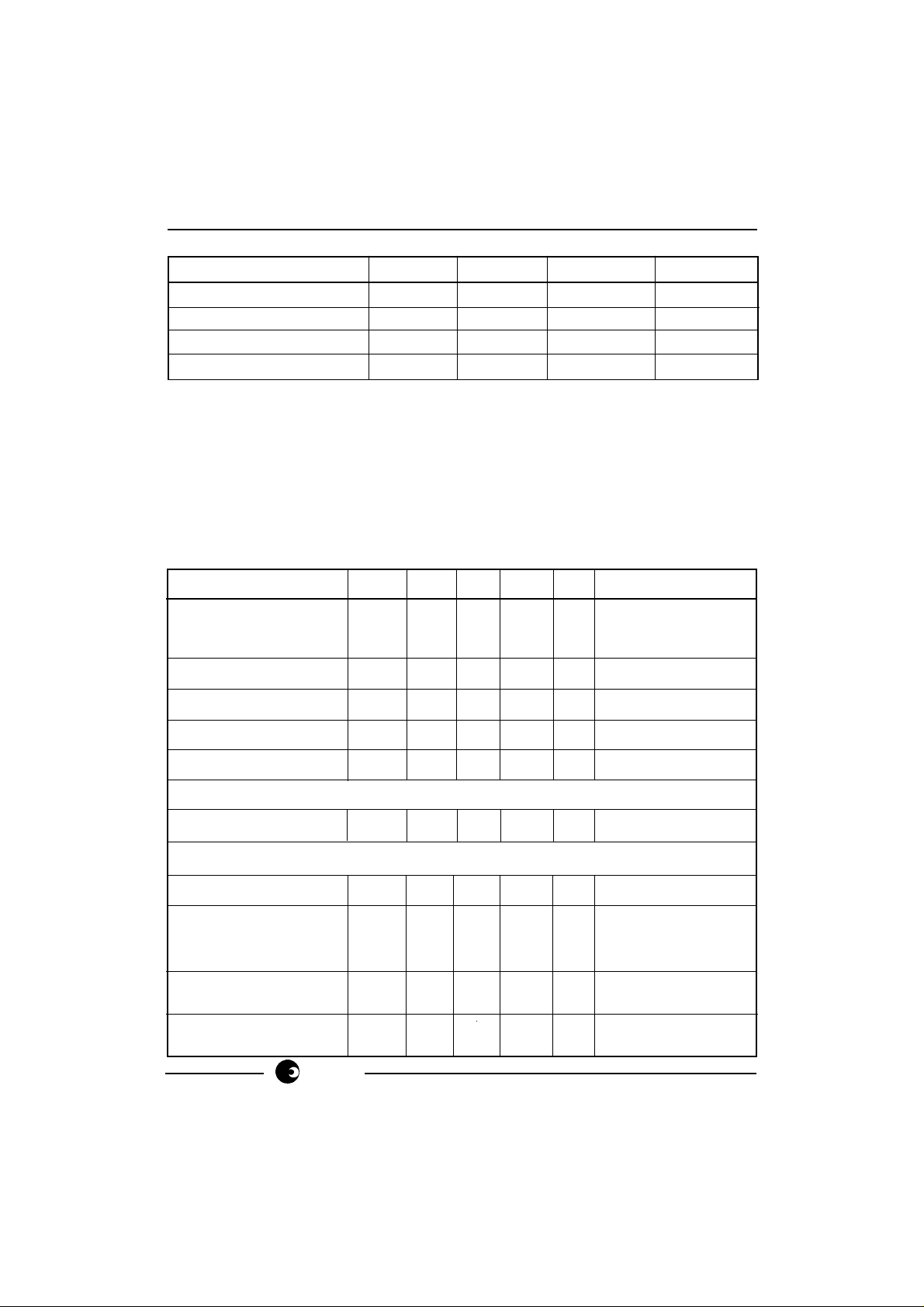
ABSOLUTE MAXIMUM RATINGS*
Parameter Symbol Min Max Unit
Supply Voltage VDD -V
Current on any pin I
Storage Temperature T
Operating Temperature T
PIN
STG
O
SS
-0.3 6.0 V
-150 +150 mA
-40 +125 °C
-40 +85 °C
* Stresses above those listed under “Absolute Maximum Ratings” may cause permanent
damage to the device. This is a stress rating only. Functional operation of the device
at these or any other condition above those indicated in the operational sections of this
specification, is not implied. Exposure to Absolute Maximum Ratings for extended
periods may affect device reliability.
ELECTRICAL CHARACTERISTICS
(VDD = 2.5V, VSS = -2.5V, over the temperature range -10°C to +70°C#, unless otherwise
specified.)
Parameter Symbol Min Typ Max Unit Condition
Operating temperature
#
range
Supply Voltage: Positive V
Supply Voltage: Negative V
Supply Current: Positive I
Supply Current: Negative I
T
-25 +85 °C
O
2.25 2.75 V
DD
-2.75 -2.25 V
SS
DD
SS
56mA
56mA
Current Sensor Inputs (Differential)
Input Current Range I
II
Voltage Sensor Input (Asymmetrical)
Input Current Range I
IV
Pins FOUT, FOUT2
Output Low Voltage V
Output High Voltage V
Pulse Rate FOUT f
Pulse Width tp t
OL
OHVDD
P
PP
t
pn
sames
-25 +25 µA Peak value
-25 +25 µA Peak value
VSS+1 V IOL = 5mA
-1 V IOH = -2mA
0 1160 Hz Specified linearity
0 3000 Hz Min and max limits
71.55 µs Positive Energy Flow
143.1 µs Negative Energy Flow
3/14
Page 4
SA9602H
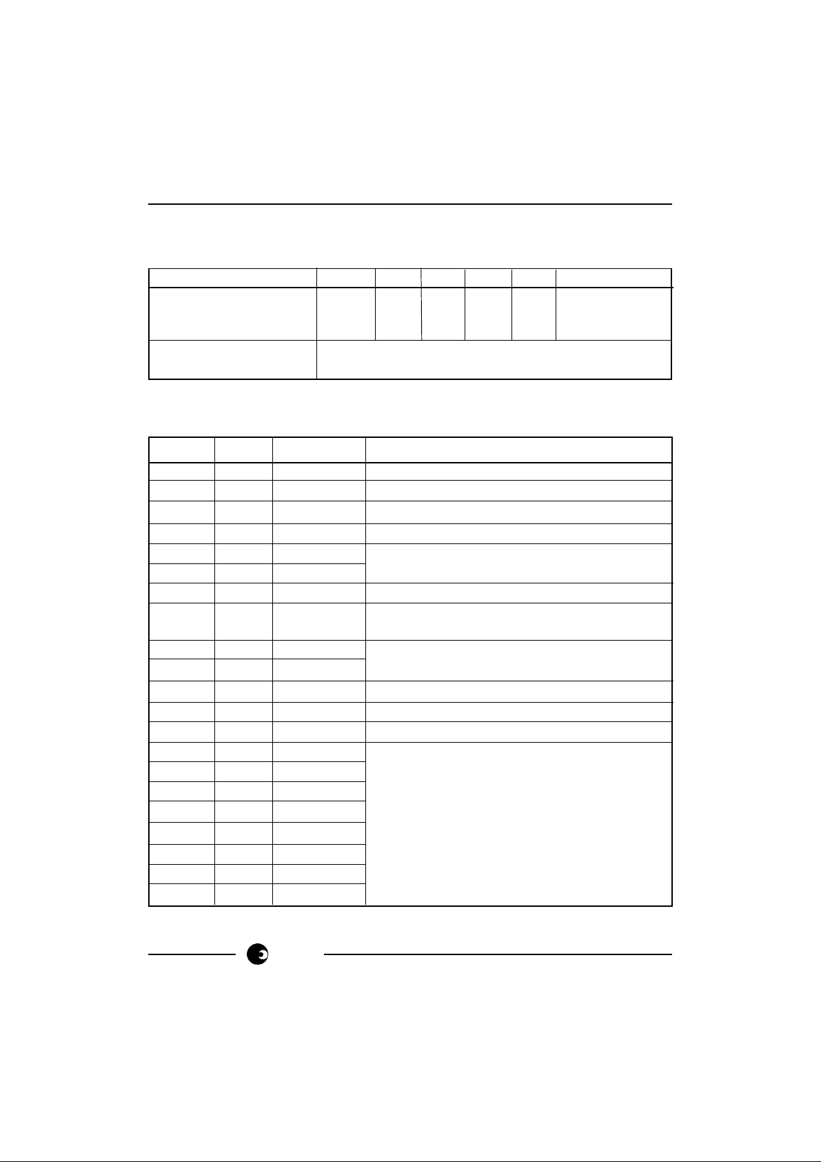
ELECTRICAL CHARACTERISTICS (Continued)
(VDD = 2.5V, VSS = -2.5V, over the temperature range -10°C to +70°C#, unless otherwise
specified.)
Parameter Symbol Min Typ Max Unit Condition
Pin VREF With R = 24kΩ
Ref. Current -I
Ref. Voltage V
R
R
45 50 55 µA connected to V
1.1 1.3 V Referred to V
SS
SS
Oscillator Recommended crystal:
TV colour burst crystal f = 3.5795 MHz
#
Extended Operating Temperature Range available on request.
PIN DESCRIPTION
14 Pin 20 Pin Designation Description
14 20 GND Ground
5 8 V
10 14 V
DD
SS
Positive Supply Voltage
Negative Supply Voltage
13 19 IVP Analog input for Voltage
1 1 IIN Inputs for current sensor
2 2 IIP
3 3 VREF Connection for current setting resistor
4 7 TEST Test Pin. Tie to VSS for protection against HV
transients and noise
7 11 OSC1 Connections for crystal or ceramic resonator
6 10 OSC2 (OSC1 = Input ; OSC2 = Output)
8 12 FOUT Pulse rate output
9 13 DIR Direction indication output
11 15 FMO Rising edge of mains frequency
4 TP4 Test Pins (Leave unconnected)
5 TP5
6 TP6
9 TP9
12 TP12
16 TP16
17 TP17
18 TP18
4/14
sames
Page 5

SA9602H
FUNCTIONAL DESCRIPTION
The SA9602H is a CMOS mixed signal Analog/Digital integrated circuit, which performs
power/energy calculations across a power range of 1000:1, to an overall accurancy of
better than Class 1.
The integrated circuit includes all the required functions for 1-phase power and energy
measurement such as two oversampling A/D converters for the voltage and current sense
inputs, power calculation and energy integration. Internal offsets are eliminated through
the use of cancellation procedures. The SA9602H generates pulses, the frequency of
which is proportional to the power consumption. The pulse rate follows the instataneous
power consumption measured. Direction information is also provided.
A voltage zero crossover signal, relevant to the positive going half cycle, is available on
pin FMO. This signal can be used to sychronise circuit breaker switching.
1. Power Calculation
In the Application Circuit (Figure 1), the voltage drop across the shunt will be between
0 and 16mV
converted to a current of between 0 and 16µA
(0 to 80A through a shunt resistor of 200µΩ). This voltage is
RMS
, by means of resistors R1 and R2.
RMS
The current sense input saturates at an input current of ±25µA peak.
For the voltage sensor input, the mains voltage (230VAC) is divided down through
a divider to 14V. The current into the A/D converter input is set at 14µA
at nominal
RMS
mains voltage, via resistor R4 (1MΩ).
In this configuration, with a mains voltage of 230V and a current of 80A, the output
frequency of the SA9602H power meter chip at FOUT is 1.16kHz. In this case 1 pulse
will correspond to an energy consumption of 18.4kW/1160Hz = 15.9Ws.
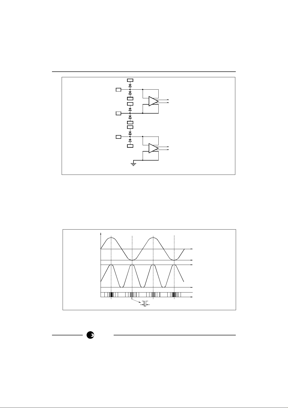
2. Analog Input Configuration
The input circuitry of the current and voltage sensor inputs are illustrated below.
These inputs are protected against electrostatic discharge through clamping diodes.
The feedback loops from the outputs of the amplifiers AI and AV generate virtual
shorts on the signal inputs. Exact duplications of the input currents are generated
for the analog signal processing circuitry.
sames
5/14
Page 6
SA9602H
IIP
CURRENT
SENSOR
INPUT S
IIN
IVP
VOLTAGE
SENSOR
INPUT
V
DD
V
SS
V
DD
V
SS
V
DD
V
SS
A
A
I
V
DR-01279
GND
3. Electrostatic Discharge (ESD) Protection
The SA9602H integrated circuit's inputs/outputs are protected against ESD
4. Power Consumption
The power consumption rating of the SA9602H integrated circuit is less than 25mW.
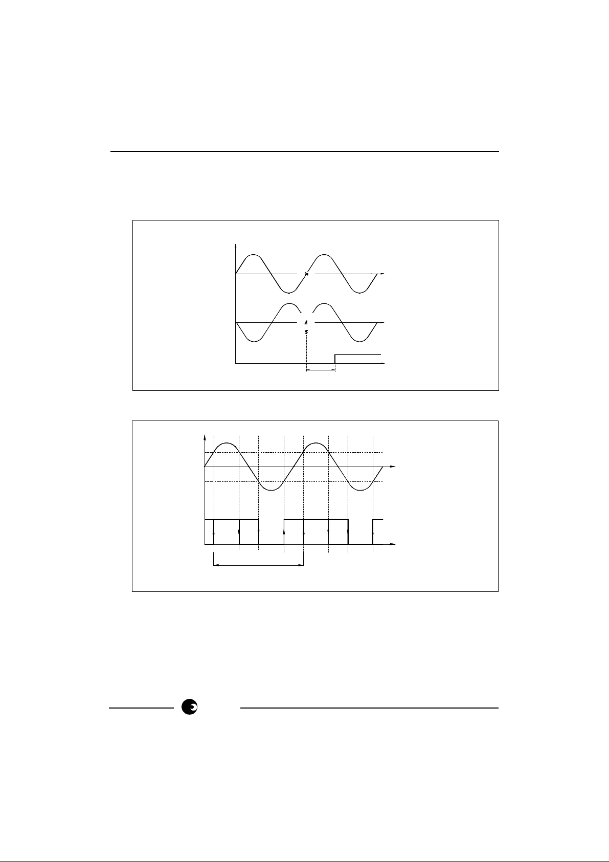
5. Pulse Output Signals
The diagram below shows the behavior of the instantaneous pulse output, FOUT,
with respect to the power consumption.
v
MAIN S
t
POWER
V x I
t
FOUT
DR-01282
t
P
t
6/14
sames
Page 7
SA9602H
The diagram below shows the behavior of the direction indicator, DIR, when energy
reversal takes place. The timing period for the DIR signal to change state, t
DIR
, will
be defined by the time it takes for the integrater to count down from its value at the
time of energy reversal. This is determined by the energy consumption rate.
I
V
DIR
DR -01283
t
DIR
t
t
t
The square wave signal on FMO indicates the polarity of the mains voltage.
V
t
FM O
t
t
MAINS
DR-01284
Due to comparator offsets, the FMO low to high transition can occur within a
range as shown above. The time between succesive low to high transitions will
be equal to the mains voltage period.
sames
7/14
Page 8

SA9602H
TYPICAL APPLICATIONS
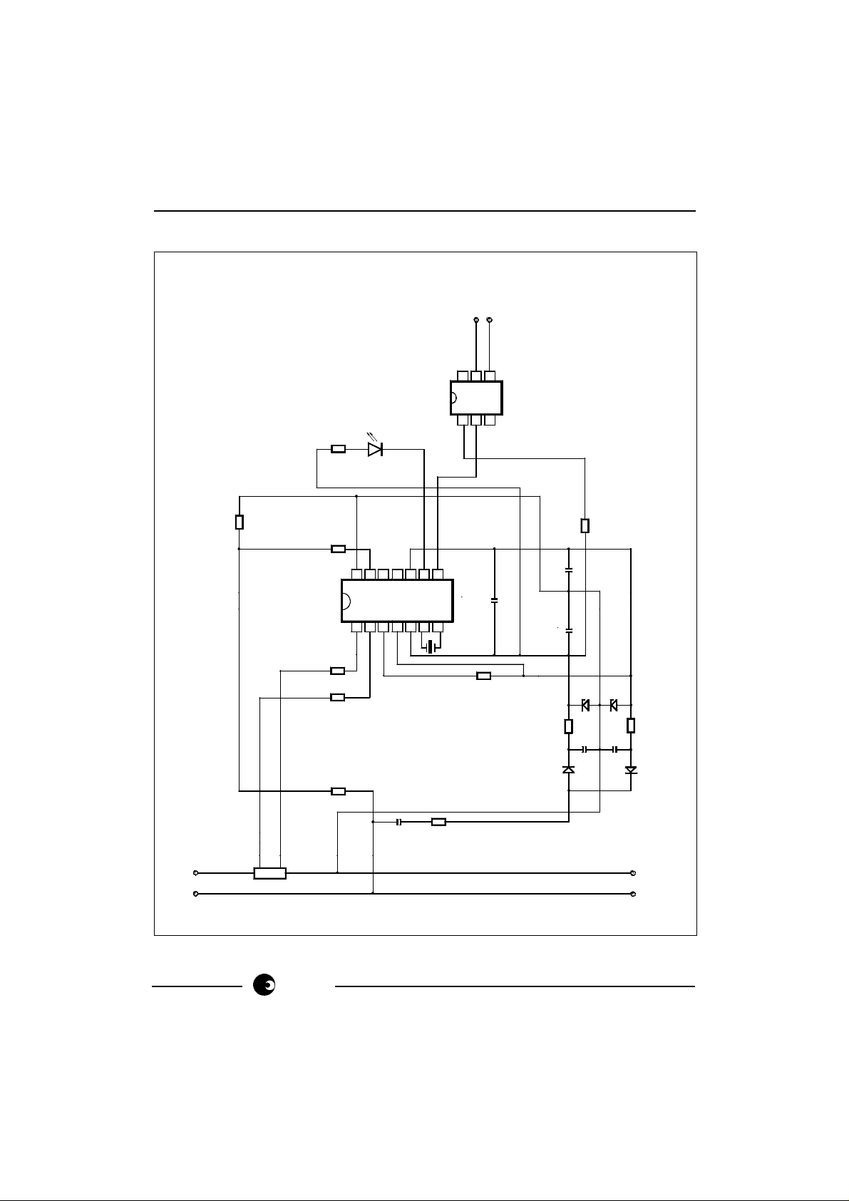
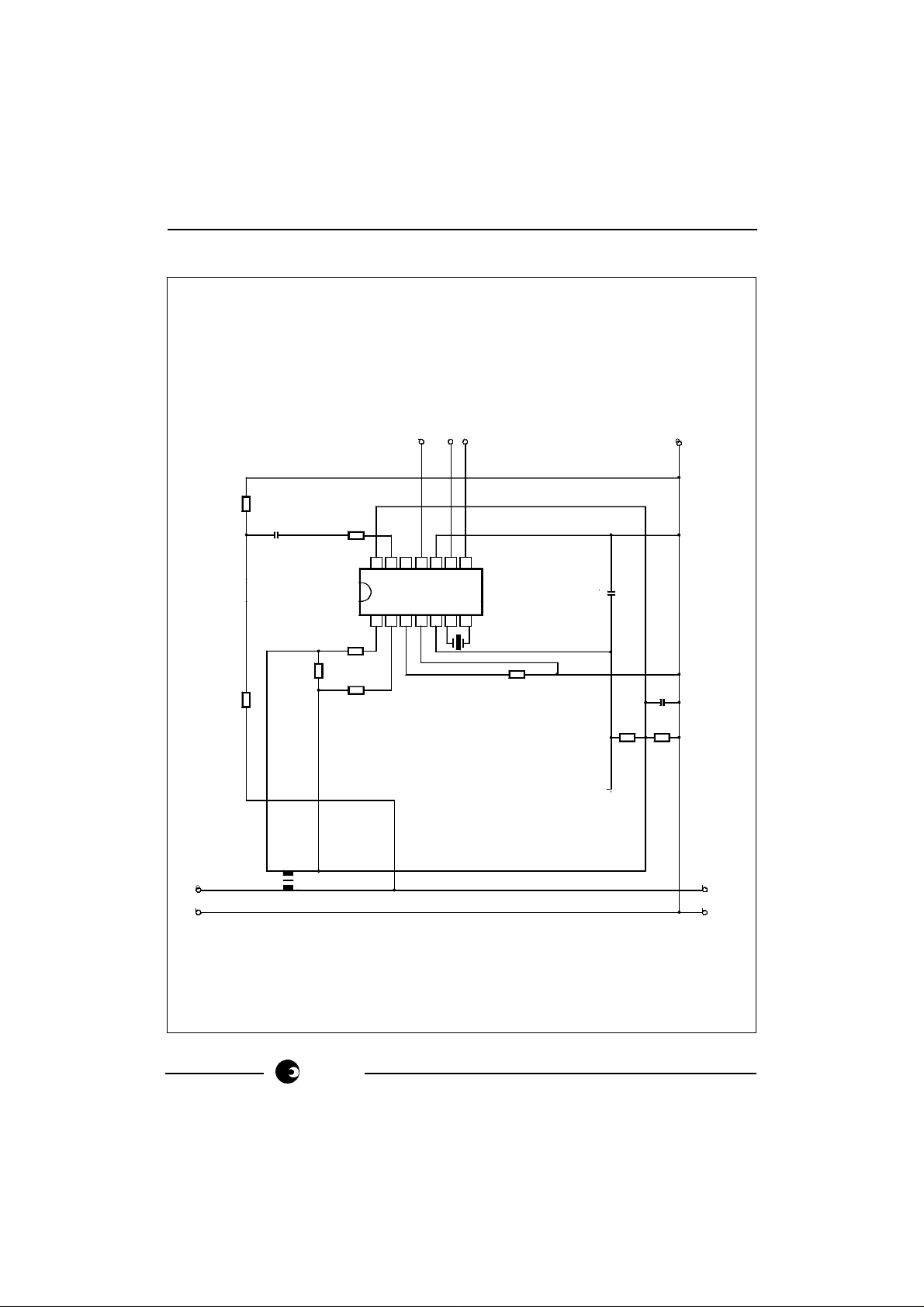
In the Application Circuits (Figures 1 and 2), the components required for power metering
applications, are shown.
In Figure 1 a shunt resistor is used for current sensing. In this application, the circuitry
requires a +2.5V, 0V, -2.5V DC supply.
In the case of Figure 2, when using a current transformer for current sensing, a +5V, 0V
DC supply is sufficient.
The most important external components for the SA9602H integrated circuit are:
R2, R1 and RSH are the resistors defining the current level into the current sense input. The
values should be selected for an input current of 16µA
into the SA9602H at maximum
RMS
line current.
Values for RSH of less than 200µΩ should be avoided.
R1 = R2 = (IL/16µA)
Where I
L
* RSH/2
RMS
= Line current
RSH = Shunt resistor/termination resistor
R3, R6 and R4 set the current for the voltage sense input. The values should be selected
so that the input current into the voltage sense input (virtual ground) is set to 14µA
RMS
R7 defines all on-chip bias and reference currents. With R7 = 24kΩ, optimum conditions
are set. R7 may be varied within ±10% for calibration purposes. Any change to R7 will affect
the output quadratically (i.e.: R7 = +5%, fP = +10%).
The formula for calculating the output frequency is given below:
f = 11.16
FOUTX
*
3.58MHz I
FOSC * II .I
*
V
2
R
Where FOUTX = Normal rated frequency (1160Hz)
.
FOSC = Oscillator frequency (2MHz ...... 4MHz)
I
I
I
V
I
R
= Input current for current input (16µA
= Input current for voltage input (14µA
RMS
RMS
= Reference current (typically 50µA)
at rated)
at rated)
XTAL is a colour burst TV crystal (f = 3.5795 MHz) for the oscillator. The oscillator
frequency is divided down to 1.7897 MHz on-chip, to supply the digital circuitry and the A/
D converters.
8/14
sames
Page 9
SA9602H
Figure 1: Application Circuit using a Shunt Resistor for Current Sensing.
NC
6
4
5
IC-2
3
2
1
R11
LED
NC
R6
R8
R4
14
1
13
2
12
3
11
IC-1
4
10
5
9
C15
7
6
C10
C9
DR-01280
8
XTAL
R1
R7
ZD1
ZD2
R2
R9
C13
D1
RSH
R3
R5
C11
LOAD
C14
R10
D2
SUPPLY
sames
9/14
Page 10

SA9602H
Parts List for Application Circuit: Figure 1
Item Symbol Description Detail
1 IC-1 SA9602H DIP-14
2 IC-2 Optocoupler 4N35 DIP-6
3 D1 Diode, Silicon, 1N4148
4 D2 Diode, Silicon, 1N4148
5 ZD1 Diode, Zener, 2.4V, 200mW
6 ZD2 Diode, Zener, 2.4V, 200mW
7 XTAL Crystal, 3.5795MHz Colour burst TV
8 R1 Resistor, 1% metal Note 1
9 R2 Resistor, 1% metal Note 1
10 R3 Resistor, 390k, (230VAC) 1%, metal
11 R4 Resistor, 1M, 1/4W, 1%, metal
12 R5 Resistor, 470Ω, 2W, 5%, carbon
13 R6 Resistor, 24k, 1/4W, 1%, metal
14 R7 Resistor, 24k, 1/4W, 1%, metal
15 R8 Resistor, 680Ω, 1/4W, 1%
16 R9 Resistor, 680Ω, 1/4W, 1%
17 R10 Resistor, 680Ω, 1/4W, 1%
18 R11 Resistor, 2.2K, 1/4W, 1%
19 C9 Capacitor, 100nF
20 C10 Capacitor, 100nF
21 C11 Capacitor, 0.47µF, 250VAC, polyester
22 C13 Capacitor, 100µF
23 C14 Capacitor, 100µF
24 C15 Capacitor, 820nF Note 2
25 RS H Shunt Resistor Note 3
26 LED Light Emitting Diode
Note 1: Resistor (R1 and R2) values are dependant upon the selected value of RSH.
Note 2: Capacitor (C15) to be positioned as close to Supply Pins (VDD & VSS) of IC-1 as
possible.
Note 3: See TYPICAL APPLICATIONS when selecting the value of RSH.
10/14
sames
Page 11
SA9602H
Figure 2: Application Circuit using a Current Transformer for Current Sensing.
DIR
FOUT
R6
FM O
C1 1
R4
0V
R3
14
13
12
1
3
2
R1
RS H
R2
11
IC-1
4
10
5
8
9
C9
7
6
XT AL
R7
C1 0
R2
R8
R9
=
RSH = T ERM INAT ION RESIS TOR FOR CURRENT T RANSFORM ER
R1
5V
CT
2.4 V TO 2.6V DC
DR-01281
L
LOAD
N
SUPPL Y
sames
11/14
Page 12

SA9602H
Parts List for Application Circuit: Figure 2
Item Symbol Description Detail
1 IC-1 SA9602H DIP-14
2 XTAL Crystal, 3.5795MHz Colour burst TV
3 RSH Resistor Note 1
4 R1 Resistor, 1%, metal Note 2
5 R2 Resistor, 1%, metal Note 2
6 R3 Resistor, 390k, (230VAC), 1%, metal
7 R4 Resistor, 1M, 1/4W, 1%, metal
8 R6 Resistor, 24k, 1/4W, metal
9 R7 Resistor, 24k, 1/4W, 1%, metal
10 R8 Resistor, 2.2k, 1/4W, 1%, metal
11 R9 Resistor, 2.2k, 1/4W, 1%, metal
12 C9 Capacitor, 820nF Note 3
13 C10 Capacitor, 100nF
14 C11 Capacitor Note 4
15 CT Current transformer
Note 1: See TYPICAL APPLICATIONS when selecting the value of RSH.
Note 2: Resistor (R1and R2) values are dependant upon the selected value of RSH.
Note 3: Capacitor (C9) to be positioned as close to Supply Pins (VDD & VSS) of IC-1,
as possible.
Note 4: Capacitor (C11) selected to minimize phase error introduced by current
transformer (typically 1.5µF).
ORDERING INFORMATION
Part Number Package
SA9602HPA DIP-20
SA9602HSA SOIC-20
SA9602HPA DIP-14
Note: When ordering, the Package Option must be specified along with the Part
Number.
12/14
sames
Page 13

NOTES:
SA9602H
sames
13/14
Page 14

SA9602H
Disclaimer: The information contained in this document is confidential and proprietary to South African
Micro-Electronic Systems (Pty) Ltd ("SAMES") and may not be copied or disclosed to a third party, in whole
or in part, without the express written consent of SAMES. The information contained herein is current as of
the date of publication; however, delivery of this document shall not under any circumstances create any
implication that the information contained herein is correct as of any time subsequent to such date. SAMES
does not undertake to inform any recipient of this document of any changes in the information contained herein,
and SAMES expressly reserves the right to make changes in such information, without notification,even if such
changes would render information contained herein inaccurate or incomplete. SAMES makes no representation
or warranty that any circuit designed by reference to the information contained herein, will function without
errors and as intended by the designer.
Any sales or technical questions may be posted to our e-mail address below:
[email protected]
For the latest updates on datasheets, please visit our web site:
http://www.sames.co.za
South African Micro-Electronic Systems (Pty) Ltd
P O Box 15888, 33 Eland Street,
Lynn East, 0039 Koedoespoort Industrial Area,
Republic of South Africa, Pretoria,
Republic of South Africa
Tel: 012 333-6021 Tel: Int +27 12 333-6021
Fax: 012 333-8071 Fax: Int +27 12 333-8071
14/14
sames
 Loading...