

Page 1

SA9025
900 MHz transmit modulator and
2.2 GHz fractional–N synthesizer
Objective specification 1997 Aug 01
INTEGRATED CIRCUITS
Page 2
Philips Semiconductors Objective specification
SA9025
900 MHz transmit modulator and 2.2 GHz
fractional–N synthesizer
2
1997 Aug 01
DESCRIPTION
This specification defines the requirements for a transmitter
modulator and fractional–N synthesizer IC to be used in cellular
telephones which employ the North American Dual Mode Cellular
System (IS–136).
FEA TURES
•Low current from 3.75V supply
•Low phase noise
•Main loop with internal charge pump and fractional compensation
•3–line serial interface bus
•Power down for the synthesizers
•Speedup mode for faster switching
APPLICATIONS
•Cellular phones
•Portable battery–powered radio equipment.
GENERAL DESCRIPTION
The SA9025 BICMOS device integrates:
•Main channel synthesizer
•Auxiliary synthesizer
•Transmit offset synthesizer and oscillator
•I/Q modulator
•Power control
•Reference and clock buffers
•Control logic for programming and power down modes
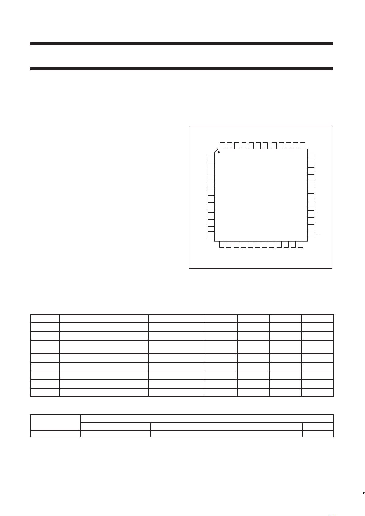
PIN CONFIGURATION
SR01446
45464748
1
2
3
4
5
6
7
13 14 15 16 17 18 19
25
26
27
28
29
30
424344
31
32
33
34
35
36
20 21 22 23 24
8
9
10
11
12
394041 3738
PHP
V
RX
GND
GND
Ipeak
TANK1
XTAL
TX
DATA
CLOCK
LOCK
STROBE
GND
I
Q
PHI
GNDRNGND
INA
GND
PHA
RCLK
MCLK
TANK2
Vcc
GND
GND
GND
GND
GND
DUAL
GND
GND
CC
V
CC
Vcc
V
CC
V
CC
V
CC
SA9025
LO1
RX
LO2
TX
LO1
TX
LO2
PHS out
TX1
DUAL
TX2
EN
2
XTAL
1
Q
I
Figure 1. Pin Configuration
QUICK REFERENCE DA TA
SYMBOL PARAMETER CONDITIONS MIN. TYP. MAX. UNIT
V
CC
Supply voltage V
CC
3.6 3.75 3.9 V
I
CC
Supply current – TBD – mA
I
CC_save
Total supply current in power–down
mode
– TBD – mA
f
VCO
Input frequency 800 – 2200 MHz
f
AUX
Input frequency 10 – 500 MHz
f
XTAL
Crystal reference input frequency 10 – 40 MHz
f
PC
Maximum phase comparator frequency Main and Aux loops – – 5 MHz
T
amb
Operating ambient temperature –40 – +85 °C
ORDERING INFORMATION
TYPE NUMBER
PACKAGE
NAME DESCRIPTION VERSION
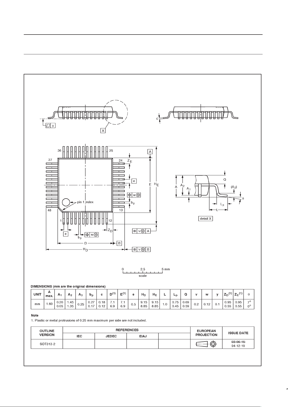
SA9025 LQFP48 Plastic low profile quad flat package; 48 leads; body 7x7x1.4 mm SOT313-2
Page 3
Philips Semiconductors Objective specification
SA9025
900 MHz transmit modulator and 2.2 GHz
fractional–N synthesizer
1997 Aug 01
3
CONNECTIONS
SR01455
PHP
V
RX
GND
GND
Ipeak
TANK1
XTAL
TX
DATA
CLOCK
LOCK
STROBE
GND
I
Q
PHI
GND
RN
GND
INA
GND
PHA
RCLK
MCLK
TANK2
GND
GND
GND
GND
GND
DUAL
GND
GND
CC
V
CC
V
CC
V
CC
V
CC
LO1
RX
LO2
TX
LO1
TX
LO2
PHS out
TX1
DUAL
TX2
EN
XTAL
V
CC
V
CC
2
MAIN
DIV.
MAIN PD
and CP
AUX.
DIV.
AUX PD
and CP
REF.
DIV.
CONTROL
LOGIC
0
90
0
90
∑
∑
0
90
∅
1
Q
I
÷M
÷N
÷A
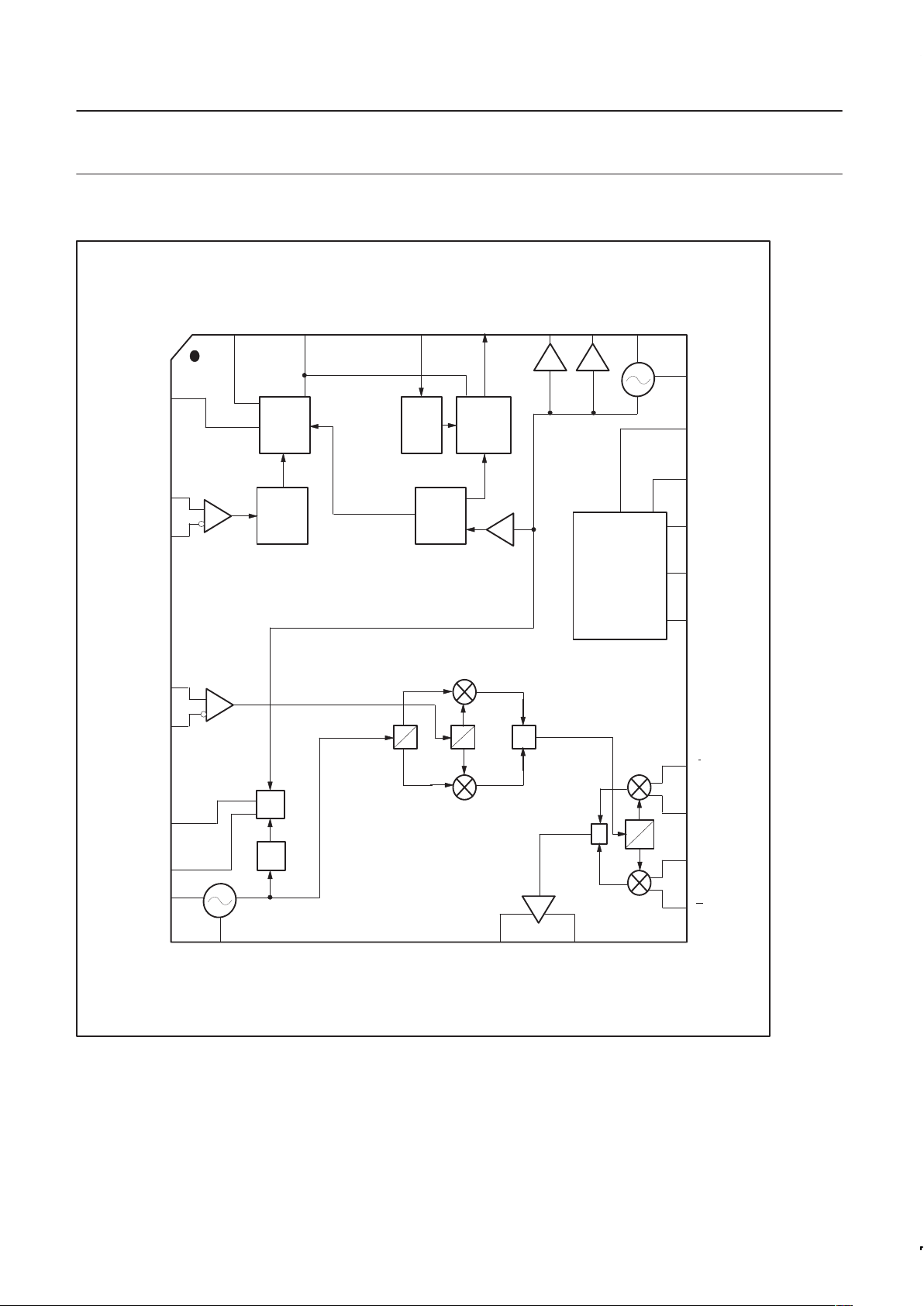
Figure 2. SA9025 Block Diagram
Page 4
Philips Semiconductors Objective specification
SA9025
900 MHz transmit modulator and 2.2 GHz
fractional–N synthesizer
1997 Aug 01
4
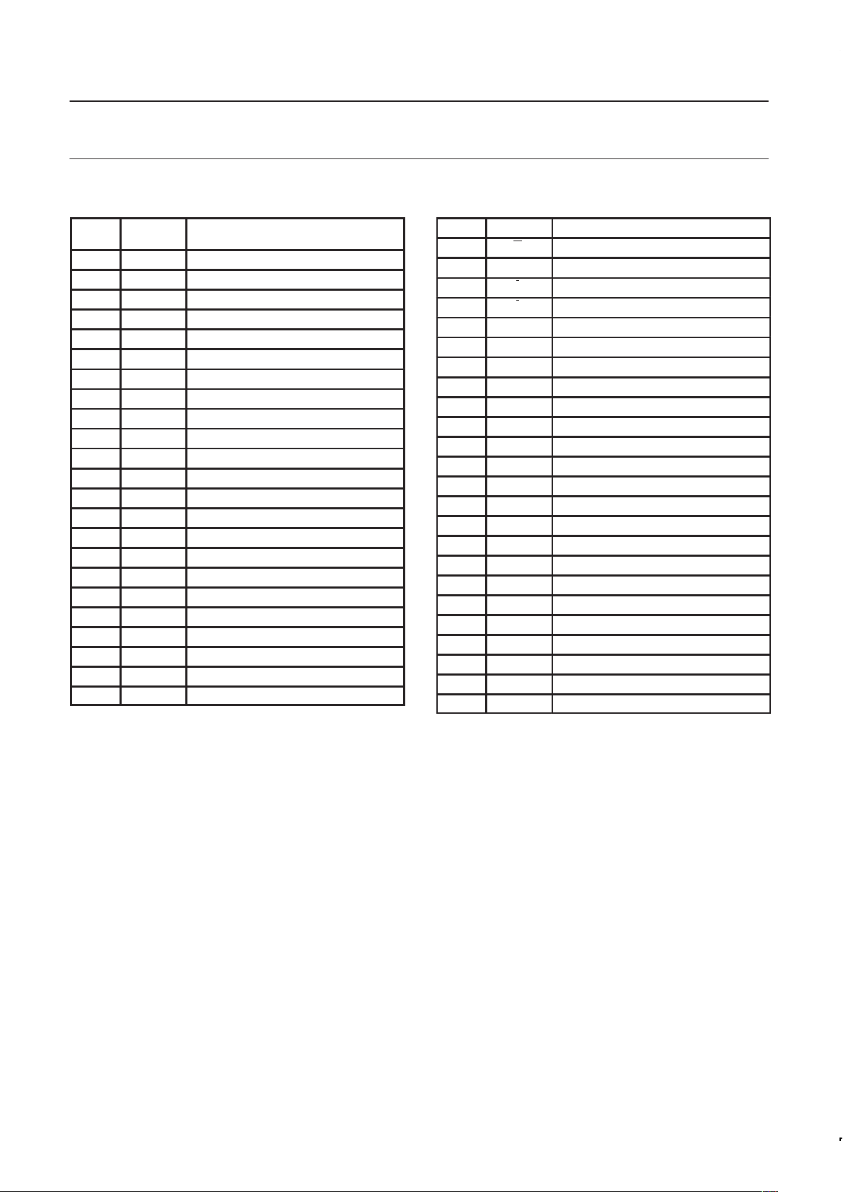
PIN DESCRIPTIONS
PIN
NO.
PIN DESCRIPTION
1 PHP Proportional charge pump output
2 V
CC
Digital supply voltage
3 RX
LO1
Differential LO input
4 RX
LO2
Differential LO input
5 GND Digital Ground
6 V
CC
Tank supply voltage
7 TX
LO1
Differential Transmit LO Input
8 TX
LO2
Differential Transmit LO Input
9 GND Tank Ground
10 PHS OUT Charge pump output (transmit offset)
11 I
PEAK
PHS out current set resistor
12 TANK1 VCO differential tank
13 TANK2 VCO differential tank
14 V
CC
Tx supply voltage
15 GND Tx Ground
16 GND Tx Ground
17 GND Tx Ground
18 GND Tx Ground
19 GND Tx Ground
20 DUALTX1 Dual mode RF output
21 GND Tx Ground
22 DUALTX2 Dual mode RF output
23 GND Tx Ground
24 V
CC
Tx supply voltage
25 Q Inverting quadrature input
26 Q Non–Inverting quadrature input
27 I Non–inverting in phase modulation input
28 I Inverting in phase modulation input
29 V
CC
Tx supply voltage
30 GND Tx Ground
31 STROBE Data input latch enable
32 LOCK Lock detect
33 CLOCK Serial clock input
34 DAT A Serial data input
35 TX
EN
Transmit enable
36 XTAL
2
Crystal Oscillator emitter input
37 XTAL
1
Crystal Oscillator base Input
38 MCLK Buffered oscillator output
39 RCLK Buffered oscillator output
40 V
CC
REF supply voltage
41 PHA Auxiliary charge pump output
42 GND REF Ground
43 INA RX
IF
input
44 V
CC
CP supply voltage
45 GND CP Ground
46 RN CP current set resistor
47 GND CP Ground
48 PHI Integral charge pump output
Page 5
Philips Semiconductors Objective specification
SA9025
900 MHz transmit modulator and 2.2 GHz
fractional–N synthesizer
1997 Aug 01
5
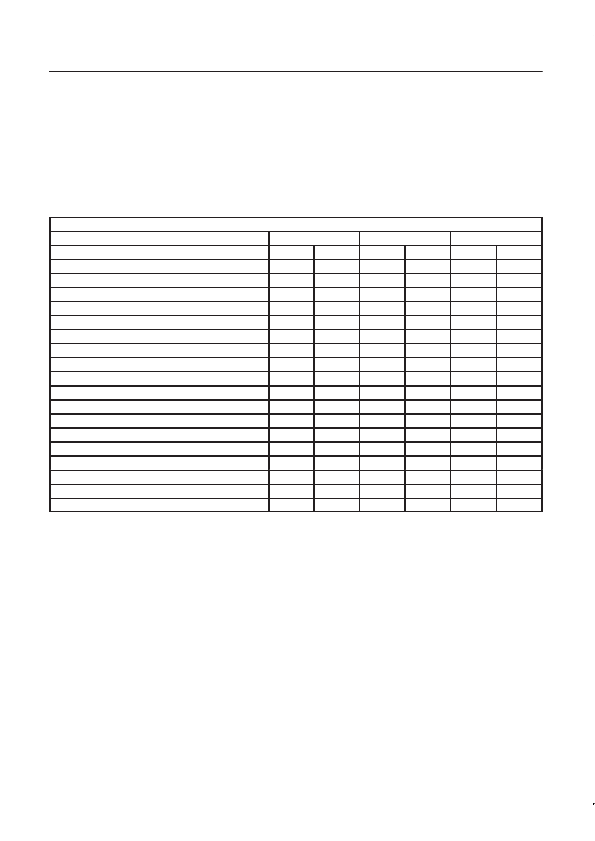
OPERATING MODES & POWER DOWN CONTROL
There are two power saving modes of operation which the SA9025
can be put into, dependent on the status of the system. The
intention of these different modes is to disable circuity that is not in
use at the time in order to reduce power consumption. During sleep
mode, only circuitry which is required to provide a master clock to
the digital portion of the system is enabled. During receive mode,
circuitry which is used to perform the receive function and provide a
master clock is enabled. In transmit mode all the functions of the
chip are enabled which are required to perform transmit, receive and
provide master clock.
SA9025 POWER MODE TRUTH TABLE
Sleep Mode Receive Mode Transmit Mode
Enabled yes no yes no yes no
Crystal Oscillator
✓ ✓ ✓
Phase detector and charge pump (transmit offset)
✓ ✓ ✓
VCO
✓ ✓ ✓
SSB Up-converter
✓ ✓ ✓
MCLK Buffer
✓ ✓ ✓
RCLK Buffer
✓ ✓ ✓
÷M offset loop divider
✓ ✓ ✓
TXLO Buffer
✓ ✓ ✓
RXLO Buffer
✓ ✓ ✓
I/Q Modulator
✓ ✓ ✓
Variable Gain Amp.
✓ ✓ ✓
Control Logic
✓ ✓ ✓
Main Divider
✓ ✓ ✓
Reference Divider
✓ ✓ ✓
Auxiliary Divider
✓ ✓ ✓
Main Phase Detector and charge pump
✓ ✓ ✓
Auxiliary Phase Detector and charge pump
✓ ✓ ✓
Lock Detect
✓ ✓ ✓
Page 6
Philips Semiconductors Objective specification
SA9025
900 MHz transmit modulator and 2.2 GHz
fractional–N synthesizer
1997 Aug 01
6
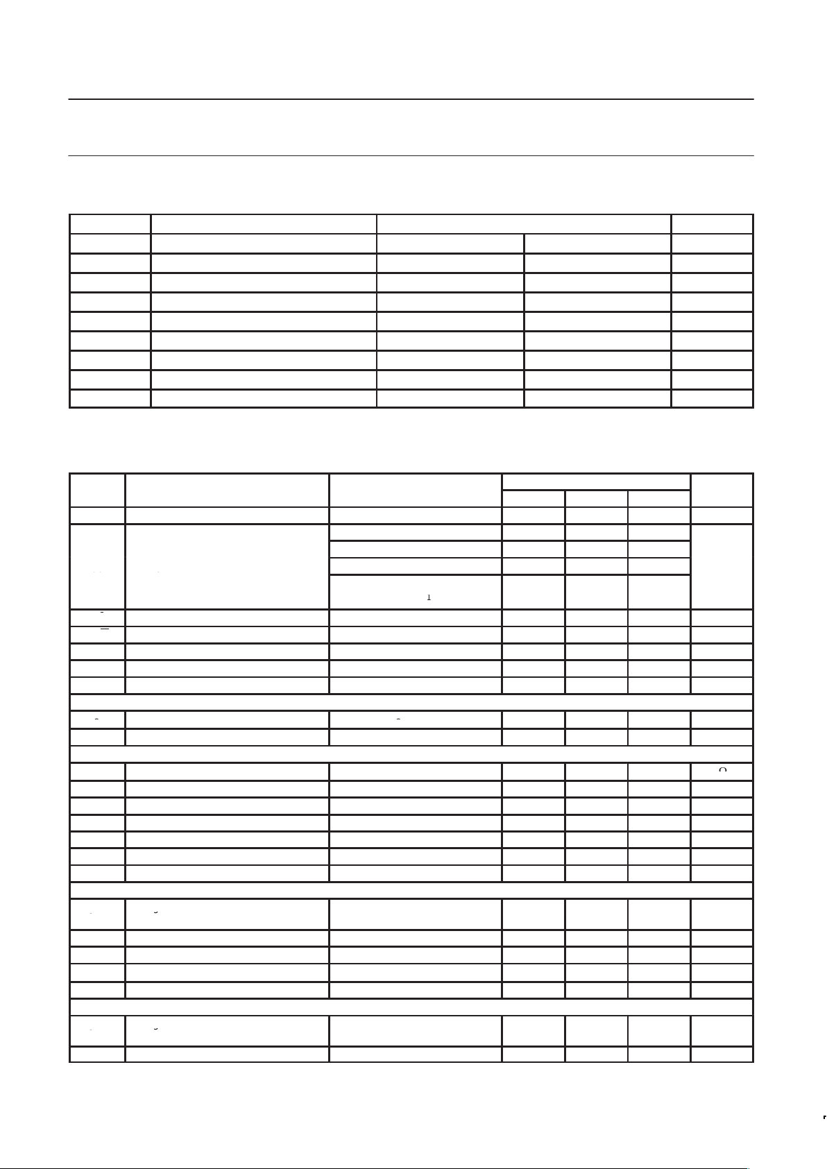
ABSOLUTE MAXIMUM RATINGS
SYMBOL PARAMETER VALUE UNIT
MIN. MAX.
V
CC
Supply voltage -0.3 +4.5 V
V
IN
Voltage applied to any other pin -0.3 VCC+0.3 V
P
N
Power dissipation, TA = 25°C (still air) 980 mW
T
JMAX
Operation junction temperature TBD °C
P
MAX
Power input/output +10/+14 dBm
I
MAX
DC current into any I/O pin -10 +10 mA
T
STG
Storage temperature –65 +150 °C
T
o
Operating temperature -40 +85 °C
DC ELECTRICAL CHARACTERISTICS
V
CC
= +3.75 V; TA = 25°C; unless otherwise stated.
SYMBO
LIMITS
L
PARAMETER
TEST CONDITIONS
MIN TYP MAX
UNITS
V
CC
Power supply range 3.6 3.75 3.9 V
Sleep mode 2
Standby mode 17
I
CC
Supply current
Operating: full power analog 95
mA
CC
y
Operating: full power digital
DUAL
1
52
I / I In-phase dif ferential input quiescent VCC /2 V
Q / Q Quadrature phase differential input quiescent VCC /2 V
V
IL
Clock, Data, Strobe, TX
EN
Input logic low –0.3 0.3 × V
CC
V
V
IH
Clock, data, strobe, TX
EN
Input logic high 0.7 × V
CC
VCC+0.3 V
T
A
Ambient temperature range -40 +25 +85 °C
Digital Outputs Lock
p
VOLOutput voltage LOW
I
O
=
2mA
0.4
V
V
OH
Output voltage HIGH IO = -2mA V
CC
– 0.4 V
Charge Pump Current Setting Resistor Input; RN, R
Ipeak
RN
External resistor to ground
6
7.5
24
k
R
Ipeak
External resistor to ground 4.7
k
V
RN
Regulated voltage
RN = 7.5 k
1.23 V
V
Ipeak
Regulated voltage
R
ipeak
= 4.7 k
1.3 V
I
peak
PHSOUT programming
R
ipeak
= 4.7 k
0.26 mA
PHS
gain
PHSOUT gain
R
ipeak
= 4.7 k
24xI
peak
mA
K
PD phase gain Transmit offset PLL in phase lock 4.33 mA/rad
Charge Pump Outputs (including fractional compensation pump, not PHS) RN = 7.5 k
Charge pump output current error
I
OPH
g
versus expected current.
–
1515%
I
MATCH
Sink to source current matching V
PHX =
VCC/2 –5 5 %
Current output variation versus V
PHX
V
PHX
in compliance range –10 10 %
Charge pump off, leakage current V
PHX
= VCC/2 –10
1
10 nA
V
PH
Charge pump voltage compliance
3
0.7 VCC – 0.8 V
Charge Pump Outputs (only PHS) R
ipeak
= 4.7 k
Charge pump output current error
I
OPH
g
versus expected current.
–
1515%
I
MATCH
Sink to source current matching V
PHS
= VCC/2 –10 10 %
Page 7
Philips Semiconductors Objective specification
SA9025
900 MHz transmit modulator and 2.2 GHz
fractional–N synthesizer
1997 Aug 01
7
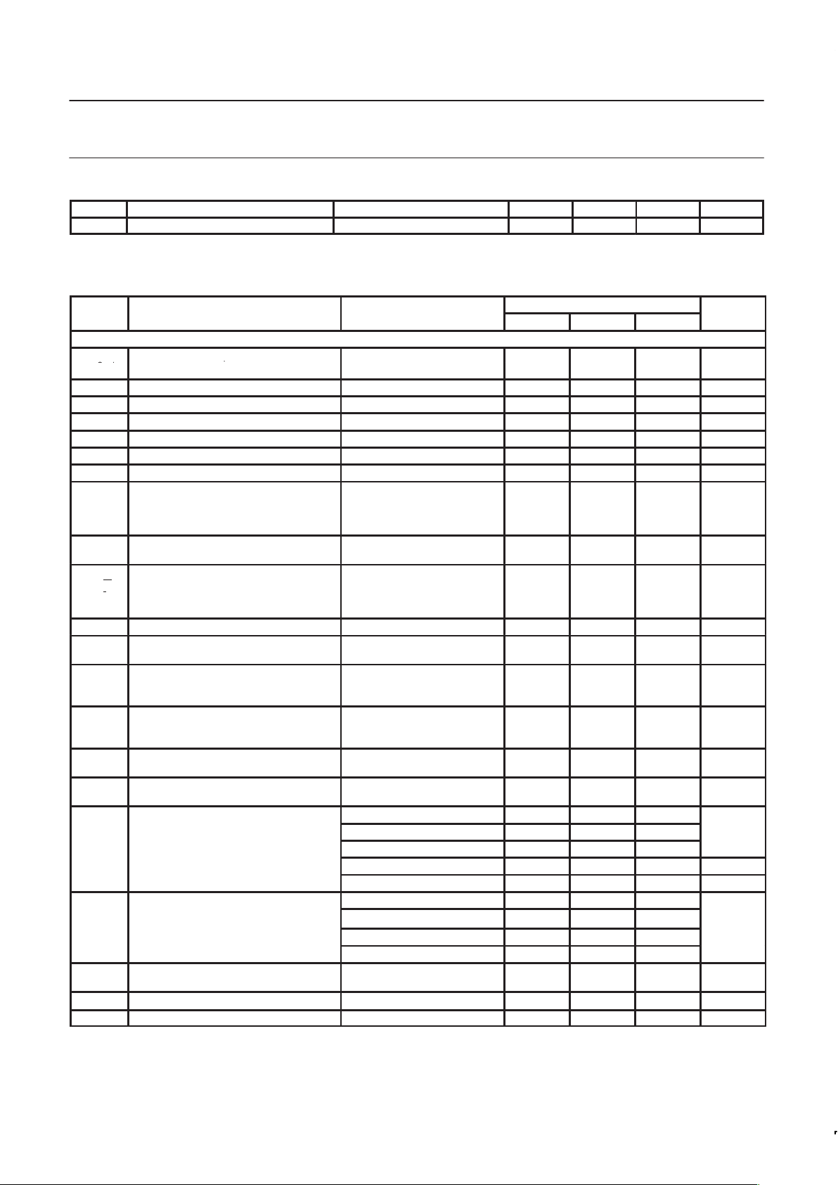
Current output variation versus V
PH
V
PHS
in compliance range –25 25 %
V
PH
Charge pump voltage compliance 0.5 VCC–0.5 V
AC ELECTRICAL CHARACTERISTICS
VCC = +3.75 V; TA = 25°C; unless otherwise stated.
LIMITS
SYMBOL
PARAMETER
TEST CONDITIONS
MIN TYP MAX
UNITS
Modulator
Transmit LO input (AC-coupled; 50Ω Input power -13 -10 dBm
TX
LO 1/2
(
single-ended, 100Ω differential) Frequency range 900 1100 MHz
VSWR 2:1
TANK1/2 VCO tank differential inputs Frequency range 90 180 MHz
÷M PLL offset divider Maximum input frequency 180 MHz
XTAL1Osc. transistor base Osc. frequency 10 40 MHz
XTAL2Osc. transistor emitter Osc. frequency 10 40 MHz
XO Negative resistance –100
RCLK,
MCLK
Reference buffer output
Frequency range
Output levels
Harmonic content
Z
LOAD
= 5kΩ| | 7 pF
10
0.7
1.0
40
1.4
–10
MHz
V
P–P
dBc
TX
EN
Transmit enable
Transmit enable
Transmit disable
TX
EN
= 1
TX
EN
= 0
Logic
Q / Q
I / I
Baseband in-phase differential inputs
Maximum frequency
Diff. mod. level
Diff. input impedance
DC bias point
1.8
0.8
10.0
1.8
0.9
VCC/2
1.0
2.55
MHz
V
P-P
kΩ
V
TX
RF
TX
RF
operating range 820 920 MHz
DUAL
TX
DUAL output SE=1, TXEN=1 (with
external matching) (50Ω)
AMPS/DAMPS 820 853 MHz
DUAL
TX
Differential output, (DUALTX)
open-collector, matched to 200Ω
differential impedance
Output level (avg. min., I and Q
quad., 0dB VGA)
Gain flatness
+9.0 +11.0
1
+13.0 dBm
dB
DUAL
TX
Linearity worst case intermod. products
(0dB VGA OR +9 dBm, whichever is
less, I & Q in-phase)
3rd-order
5th-order
7th-order
-42
-55
-65
-34
-45
-53
dBc
DUAL
TX
Carrier suppression
(I & Q in quadrature)
VGA = 0dB
VGA = -38dB
-45
-33
-35
dBc
DUAL
TX
Sideband suppression
(I & Q in quadrature)
-45 -35 dBc
2 to 284 MHz -45
824 to 849 MHz -47 dBc
DUALTXSpurious output 849 to 869 MHz -45
869 to 894 MHz -104 dBm
894 to 8490 MHz -45 dBc
TX
LO
-21
p
p
Upper Side Band –21
DUAL
TX
TX
LO
u-
conversion roducts
TXLO ±3 × TX
OFFSET
-36
dBc
Harmonics ≤ 10th -21
DUAL
TX
Broad-band noise (0dB VGA or +9 dBm,
whichever is less)
869 to 894 MHz -123 dBm/Hz
p
DUAL
TX
Adjacent channel noise power
@ 30 kH
z -
95
dBc/H
z
DUALTXAlternate channel noise power @ 60 kHz –101 dBc/Hz
Page 8
Philips Semiconductors Objective specification
SA9025
900 MHz transmit modulator and 2.2 GHz
fractional–N synthesizer
1997 Aug 01
8
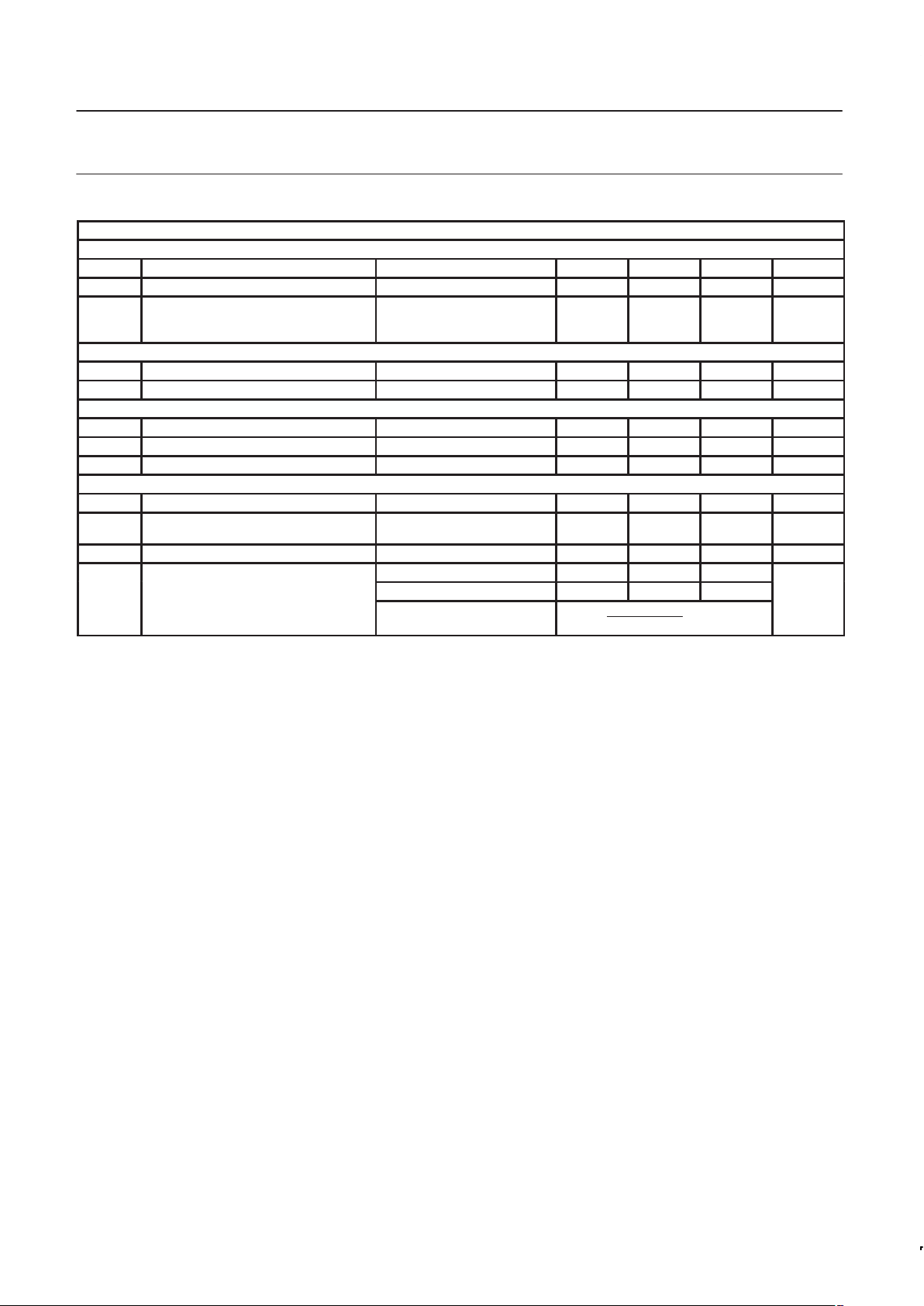
Synthesizer
Main Divider
f
MMAX
Input frequency range 800 2200 MHz
Input harmonics No multi–clocking –10 dBc
RX
LO 1/2
Synthesizer LO input (AC-coupled;
external shunt 50Ω single-ended,
100Ω differential)
Input power –20 0 dBm
Reference Divider
f
RMAX
Input frequency RANGE 10 40 MHz
Input harmonics No multi–clocking –10 dBc
Auxiliary Divider
f
AMAX
Input frequency RANGE 10 500 MHz
Input harmonics No multi–clocking –10 dBc
V
INA
Input signal amplitude 0.200 V
P-P
Serial Interface
f
CLOCK
Clock frequency 10 MHz
t
SU
Set-up time: DA TA to CLOCK, CLOCK to
STROBE
30 ns
t
H
Hold time: CLOCK to DATA 30 ns
CLOCK 30
STROBE (B - D words) 30
tSWPulse width
A word
f
1
REF
@ NREF
) t
W
ns
1. Transmit mode @ 33% duty cycle.
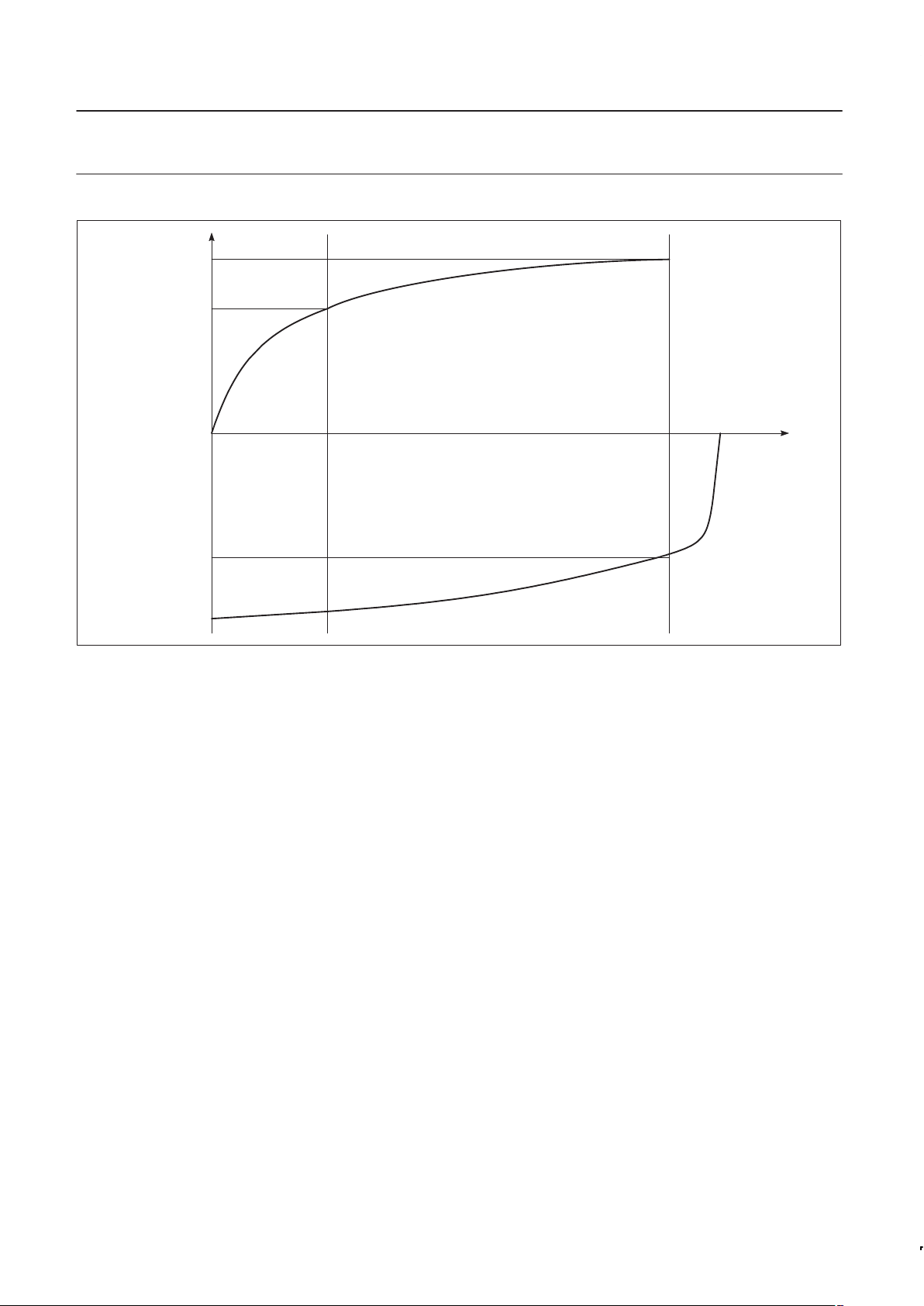
2. The relative output current variation is defined thus:
ąąDI
out/Iout
=2x(I2–I1)/|(I2+I1)|; with V1=0.7V, V2=VCC–0.8V (see figure 3)
3. Power supply current measured with ƒ
RX = 2100.54 MHZ,
ƒ
REF
= 19.44 MHz, ƒ
INA
= 109.92 MHz, main phase detector bias resistor = 7.5 kW.
Main phase detector reference frequency = 240 kHz, auxiliary phase detector frequency = 240 kHz.
4. Maximum and minimum levels guaranteed by design and random testing for temperature range of –40 to +85°C.
5. Power is rated at I/Q input level of 0.9V
PP.
Page 9
Philips Semiconductors Objective specification
SA9025
900 MHz transmit modulator and 2.2 GHz
fractional–N synthesizer
1997 Aug 01
9
I
2
I
1
I
2
I
1
V
1
V
2
CURRENT
VOLTAGE
SR00602
Figure 3. Output Current Definition
Page 10
Philips Semiconductors Objective specification
SA9025
900 MHz transmit modulator and 2.2 GHz
fractional–N synthesizer
1997 Aug 01
10
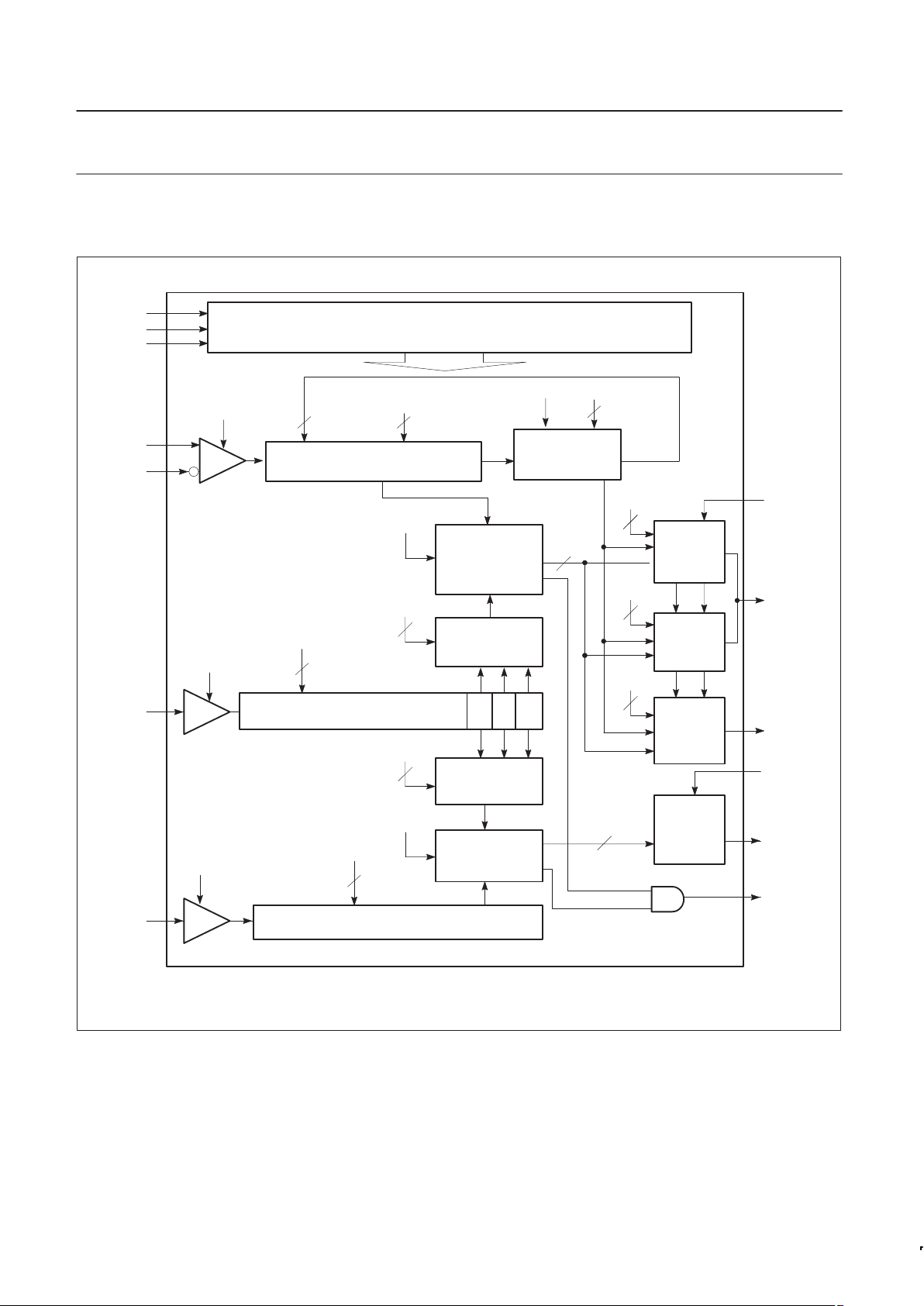
Functional Description Main Channel Synthesizer
& Auxiliary Synthesizer
SERIAL INPUT + PROGRAM LATCHES
MAIN DIVIDERS
NORMAL
OUTPUT
CHARGE
PUMP
INTEGRAL
OUTPUT
CHARGE
PUMP
AUXILIARY
OUTPUT
CHARGE
PUMP
MAIN
PHASE
DETECTOR
MAIN
REFERENCE
SELECT
SPEED-UP
OUTPUT
CHARGE
PUMP
REFERENCE DIVIDER ÷2 ÷2 ÷2
AUXILIARY
REFERENCE
SELECT
AUXILIARY
PHASE
DETECTOR
AUXILIARY DIVIDER
DATA
CLOCK
STROBE
INM1
INM2
INR
INA
FB
RN
PHP
PHI
RN
PHA
LOCK
PD1
NMAIN
FMOD
NF
16
3
FDAC
8
2
PD1
NR
PD1 + PD2
12
SA
PD2
NAUX
2
SM
PD2
2
2
14
FRACTIONAL
ACCUMULATOR
FB
1
SR01112
FDAC
8
FDAC
8
FDAC
8
Figure 4. Synthesizer Block Diagram
Serial Programming Input
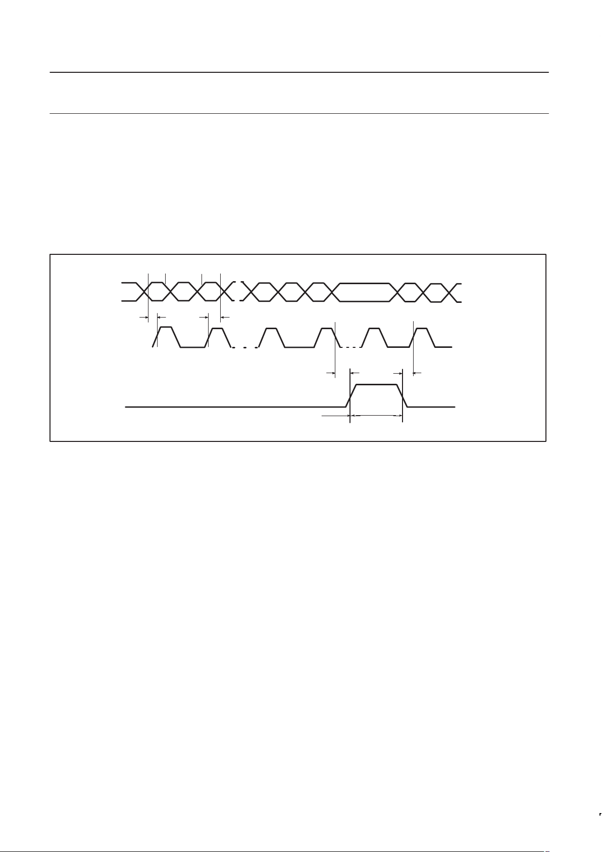
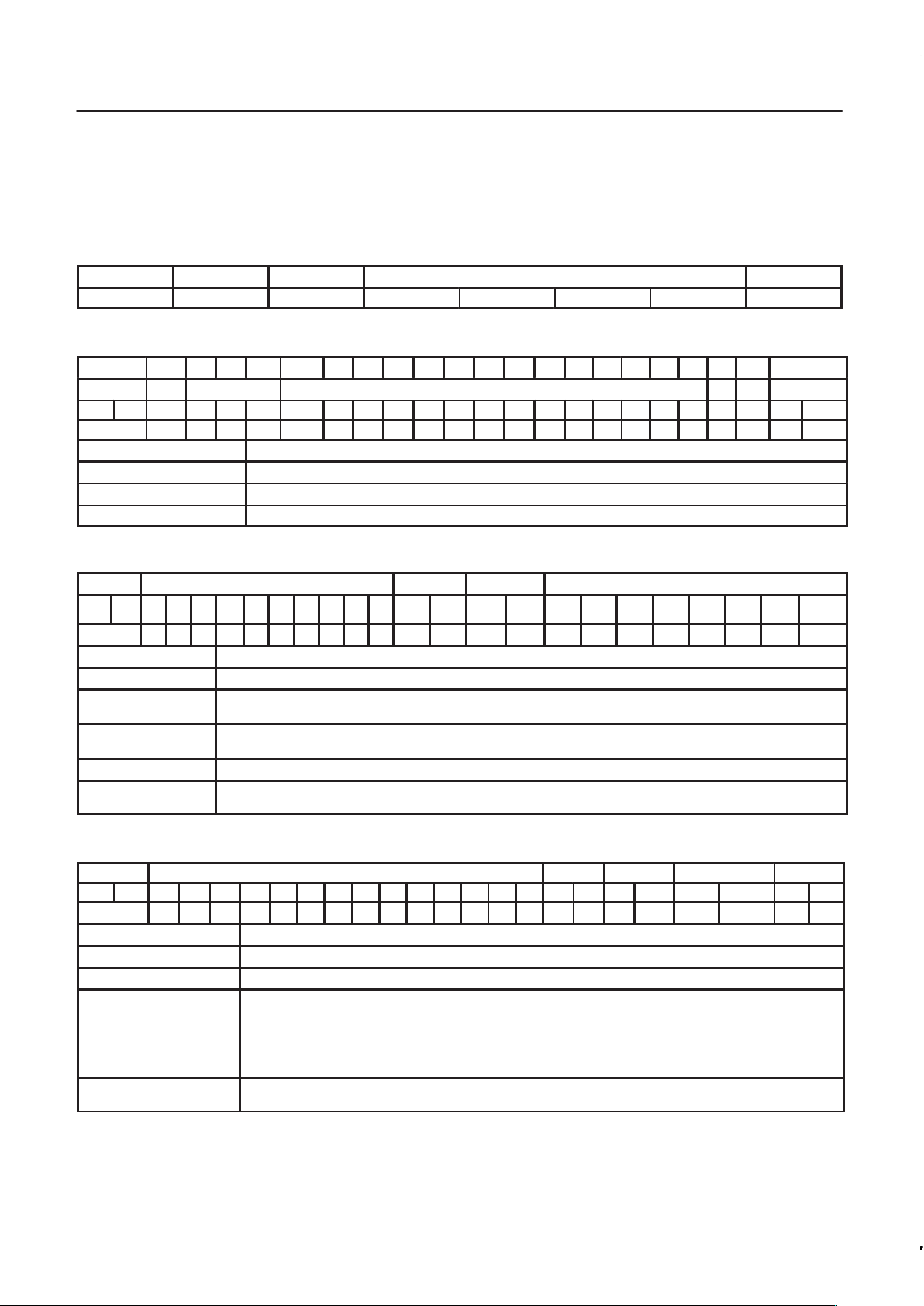
The serial input is a 3-wire input (CLOCK, DATA, STROBE) used to
program all counter ratios, DACs, selection and enable bits. The
programming data is structured into 24-bit words; each word
includes 2 or 3 address bits. Figure [5] shows the timing diagram of
the serial input. When STROBE = L, the clock driver is enabled and
on positive edges of the CLOCK, the signal on DATA input is
clocked into a shift register. When STROBE = H, the clock is
disabled and the data in the shift register remains stable.
Depending on the 2 or 3 address bits, data is latched into different
working or temporary registers. In order to fully program the
synthesizer, 3 words must be sent: A, B and C. The D word
programs all other functions within the SA9025. Those functions are
Page 11
Philips Semiconductors Objective specification
SA9025
900 MHz transmit modulator and 2.2 GHz
fractional–N synthesizer
1997 Aug 01
11
power control, ÷M (offset loop), SE (Tx
offset loop synthesizer
enable), DUAL mode, Sleep Mode 1 and Sleep Mode 2.
The data for FDAC is stored by the B word into a temporary register.
When the A word is loaded, the data in this temporary register is
loaded together with the A word into the work registers to avoid false
temporary main synthesizer output caused by changes in fractional
compensation.
The A word contains new data for the main divider. The A word is
loaded into the working registers only when a main divider
synchronization signal is active to avoid phase jumps when
reprogramming the main divider. The synchronization pulse is
generated by the main divider when it has reached its terminal
count, at which time a main divider output pulse is also sent to the
main phase detector. This disables the loading of the A word each
main divider cycle during maximum of (NREF / ƒ
REF
) seconds.
Therefore, to be sure that the A word will be correctly loaded, the
STROBE signal must be high for at least (NREF / ƒ
REF
) seconds.
When programming the A word, the main charge pumps on output
PHP and PHI are set into the speed–up mode as soon as the A
word is latched into the working registers and remain so as long as
STROBE is held high.
SR01447
DATA
D0
CLOCK
STROBE
CLOCK ENABLED–SHIFT IN DATA
CLOCK
DISABLED
STORE DATA
t
SU
LAST
CLOCK
FIRST
CLOCK
t
SU
t
H
t
SU
D1
D21 D23
D0
VALID DATA CHANGE
Figure 5. Serial Input Timing Sequence
Page 12
Philips Semiconductors Objective specification
SA9025
900 MHz transmit modulator and 2.2 GHz
fractional–N synthesizer
1997 Aug 01
12
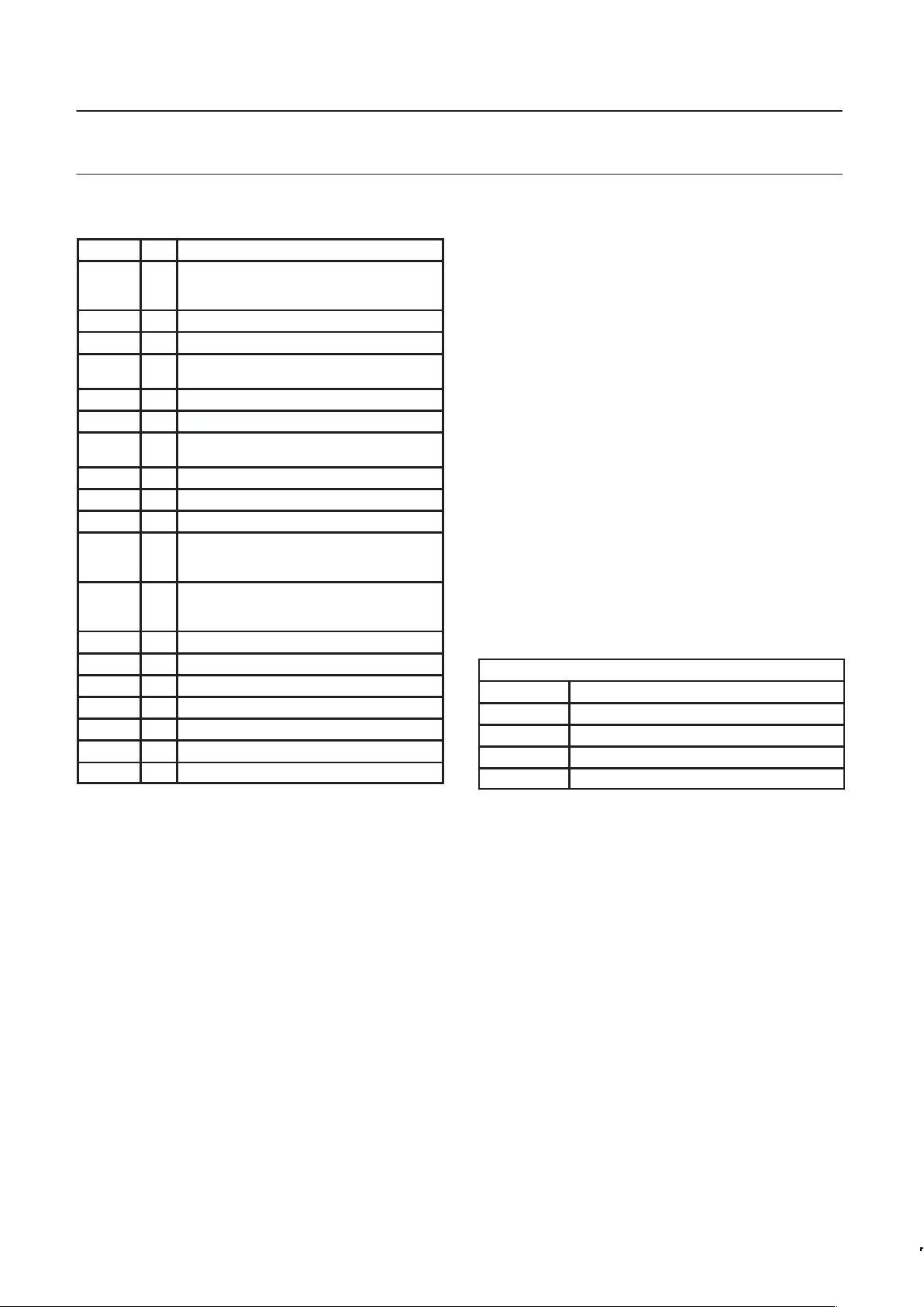
Table 1. Function Table
Symbol Bits Function
FMOD 1
Fractional-N modulus selection flag:
‘0’ = modulo 8
‘1’ = modulo 5
NF 3 Fractional-N increment
NMAIN 16 Main divider ratio; 512 to 65,535 allowed
NREF 10
Reference divider ratio; 4 to 1,023 allowed,
RSM, RSA = “0 0”
RSM 2 Reference select for main phase detector
RSA 2 Reference select for auxiliary phase detector
FDAC 8
Fractional compensation charge pump current
DAC
NAUX 14 Auxiliary divider ratio; 128 to 16,384 allowed
CP 2 Charge pump current ratio select (see table 1)
LD 2 Lock detect output select (see table 2)
PD1 1
PD1 = 0 for power down; shuts off power to
main divider and main chargepumps, anded
with PD2 to turn off ref. divider.
PD2 1
PD2 = 0 for power down; shuts off power to
auxiliary divider, and auxiliary charge pumps;
anded with PD1 to turn off ref. divider.
PC 8 Power control (see note 3)
M 2 ÷M, M = 6, 7, 8, 9 (see note 4)
SE 1 Transmit offset synthesizer on/off
TM 1 Transmit mode: ‘0’ = DUAL
AD 1 Mode control, 1 = digital; 0 = analog
SM1 1 Sleep mode 1
SM2 1 Sleep mode 2
1. Data bits are shifted in on the the leading clock edge, with the
least significant bit (LSB) first and the most significant bit (MSB)
last.
2. On the rising edge of the strobe and with the address decoder
output = 1, the contents of the input shift register are transferred
to the working registers. The strobe rising edge comes one half
clock period after the clock edge on which the MSB of a word is
shifted in.
3. The PC bits are used for the power control function. Eight (8)
bits of data allows for appropriate resolution of the power control.
00000000 = 0 dB: 11111111 = –45.9 dB (= 255 0.18).
4. The M bits are used to program the ÷M counter for integer values
between 6 and 9. 00 = 6, 01 = 7, 10 = 8, 11 = 9.
5. The TM bit is used to put the SA9025 into DUAL mode operation.
In DUAL mode (TM = 0).
6. The AD bit allows a reduction in the linearity of the DUAL output
driver while in AMPS mode.
7. The SM1 bit is used to shut down the TX
LO
buffers. SM1 = 1,
buffers on; SM1 = 0, buffers off.
8. The SM2 bit is used to shut down the RCLK buffer. SM2 = 1,
buffer on; SM2 = 0, buffer off.
9. The SE bit turns on and off the offset loop synthesizer circuits.
SE = 1, synthesizer on; SE = 0, synthesizer off.
10.The LOCK bits determine what signal is present on the LOCK
pin as follows:
Table 2.
Lock Detect Output Select*
LOCK LOCK Pin Function
00 Main, auxiliary and offset lock condition
01 Main and auxiliary lock condition
10 Main lock detect condition
11 Auxiliary lock condition
*When a section is in power down mode, the lock indicator for that
section is high.
Page 13
Philips Semiconductors Objective specification
SA9025
900 MHz transmit modulator and 2.2 GHz
fractional–N synthesizer
1997 Aug 01
13
SR01449
D Q
CLK
(1)
DQ
CLK
R
Q
D
V
CC
TX
EN
TEMPORARY REGISTER
SE
SYN
EN
(2)
CLOCK
DATA
WORKING REGISTER
R
Q
STROBE
Q
Q
R
CLK
(2)
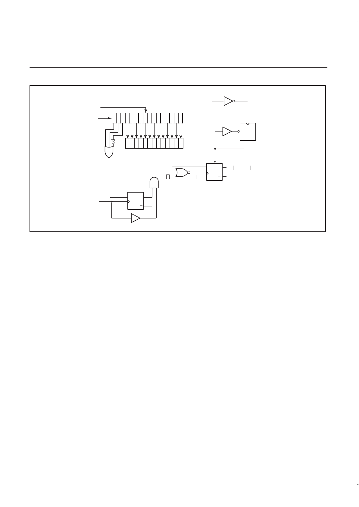
Figure 6. Transmit Offset Synthesizer Reset Circuit
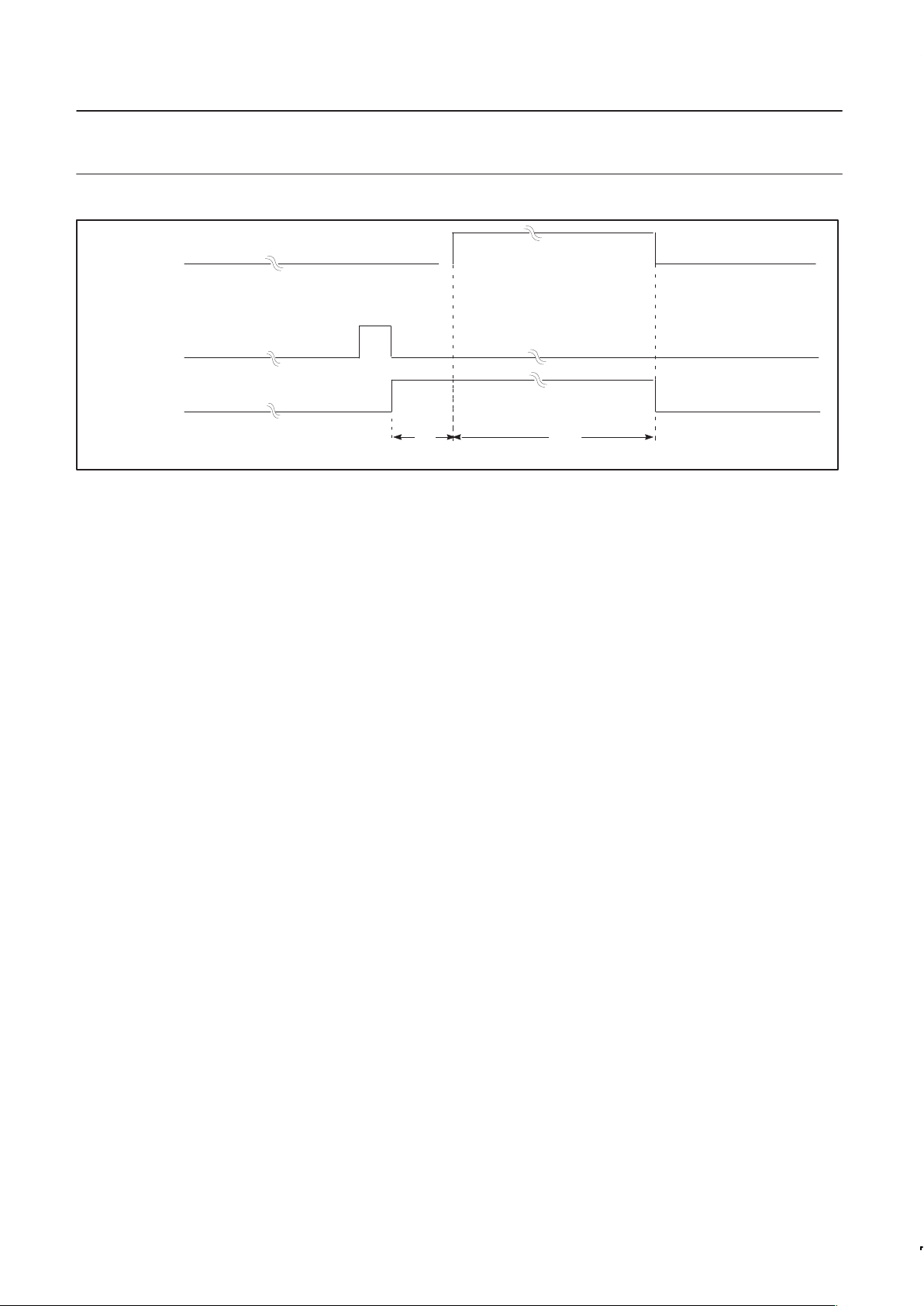
In Figure 6, the falling edge of the strobe and address, inverted,
toggles the Q output of flip-flop (1) to a ‘1’ state, enabling the phase
detector, VCO, divide by M, TX
IF
buffer and SSB up-converter.
Approximately 80µs after the synthesizer is locked, the TX
EN
signal
(enabled = 1) turns on the modulator and variable gain amplifier.
The rising edge of TX
EN
has no effect on SYNEN, however, the
falling (rising inverted) edge toggles the Q
output of D flip-flop (2) to
a ‘0’ state. This disables the synthesizer, modulator and variable
gain amplifier. To insure that slow edges on TX
EN
do not cause
improper operation, the TX
EN
is a Schmitt trigger design.
The address decoder for program word ‘D’ ANDed together with the
strobe is used to load the contents of the temporary register into the
working registers. D flip-flop (3) is used to prevent multiple strobe
and address pulses in the event the address decoder output toggles
on garbage bits during the time the strobe remains in a ‘1’ state.
The temporary register is common to the transmit offset synthesizer,
main channel synthesizer and auxiliary synthesizer.
Page 14
Philips Semiconductors Objective specification
SA9025
900 MHz transmit modulator and 2.2 GHz
fractional–N synthesizer
1997 Aug 01
14
TXen
STROBE
SYNen
80S
6.67mS
SR01538
Figure 7. Transmit Offset Synthesizer Timing Diagram
Page 15
Philips Semiconductors Objective specification
SA9025
900 MHz transmit modulator and 2.2 GHz
fractional–N synthesizer
1997 Aug 01
15
Data format
Format of programmed data
LAST IN MSB SERIAL PROGRAMMING FORMAT FIRST IN LSB
p23 p22 p21 p20 ../.. ../.. p1 p0
A word, length 24 bits
Last in MSB LSB First IN
Address fmod Fractional–N Main Divider ratio– Nmain Spare
0 0 Fmod NF2 NF1 NF0 N15 N14 N13 N12 N11 N10 N9 N8 N7 N6 N5 N4 N3 N2 N1 N0 sk1 sk2
Default:
0 0 1 0 0 0 1 0 0 0 1 0 0 0 1 1 0 0 0 0 0 0
A word select Fixed to 00.
Fractional Modulus select FM 0=modulo 8, 1=modulo 5.
Fractional–N Increment NF2..0 Fractional N Increment values 000 to 111.
N–Divider N0..N15, Main divider values 512 to 65535 allowed for divider ratio.
B word, length 24 bits
ADDRESS
REFERENCE DIVIDER NREF RSM RSA FRACTIONAL COMPENSATION DAC
0 1 R9 R8 R7 R6 R5 R4 R3 R2 R1 R0 RSM1RSM0RSA1RSA0Fdac7Fdac6Fdac5Fdac4Fdac3Fdac2Fdac1Fdac
0
Default:
0 0 0 1 0 1 0 0 0 1 0 0 0 0 x x x x x x x x
B word select Fixed to 01
R–Divider R0..R9, Reference divider values 4 to 1023 allowed for divider ration.
Charge pump current
Ratio
CP1, CP0: Charge pump current ratio, see table of charge pump currents.
Main comparison
select
RSM Comparison divider select for main phase detector.
Aux comparison select RSA Comparison divider select for auxiliary phase detector.
Fractional
Compensation
Fdac7..0, Fractional compensation charge pump current DAC, values 0 to 255. FDAC = 77 for best op MOD8.
C word, length 24 bits
ADDRESS AUXILIARY DIVIDER NAUX CP LOCK PD SPARE
1 0 A13 A12 A11 A10 A9 A8 A7 A6 A5 A4 A3 A2 A1 A0 CP1 CP0 LD1 LD0 PD1 PD2 PD3 LOD
Default
0 0 0 0 0 1 1 1 0 0 1 0 1 0 1 1 0 0 TX
EN
TX
EN
0 0
C word select Fixed to 10
A–Divider A0..A13, Auxiliary divider values 128 to 16384 allowed for divider ratio.
Charge pump current Ratio CP1, CP0: Charge pump current ratio, see table fo charge pump currents.
Lock detect output LD1 LD0
0 0 Combined main, aux. & offset loop lock detect signal present at the LOCK pin.
0 1 Combined main and aux. lock detect signal present at the LOCK pin.
1 0 Main lock detect signal present at the LOCK pin.
1 1 Auxiliary loop lock detect signal present at the LOCK pin.
When a section is in power down mode, the lock indicator for that section is high.
Power down PD1=1: power to N–divider, reference divider, main charge pumps, PD1=0 to power down.
PD2=1: power to Aux divider, reference divider, Aux charge pump, PD2=0 to power down.
Page 16
Philips Semiconductors Objective specification
SA9025
900 MHz transmit modulator and 2.2 GHz
fractional–N synthesizer
1997 Aug 01
16
Table 3.
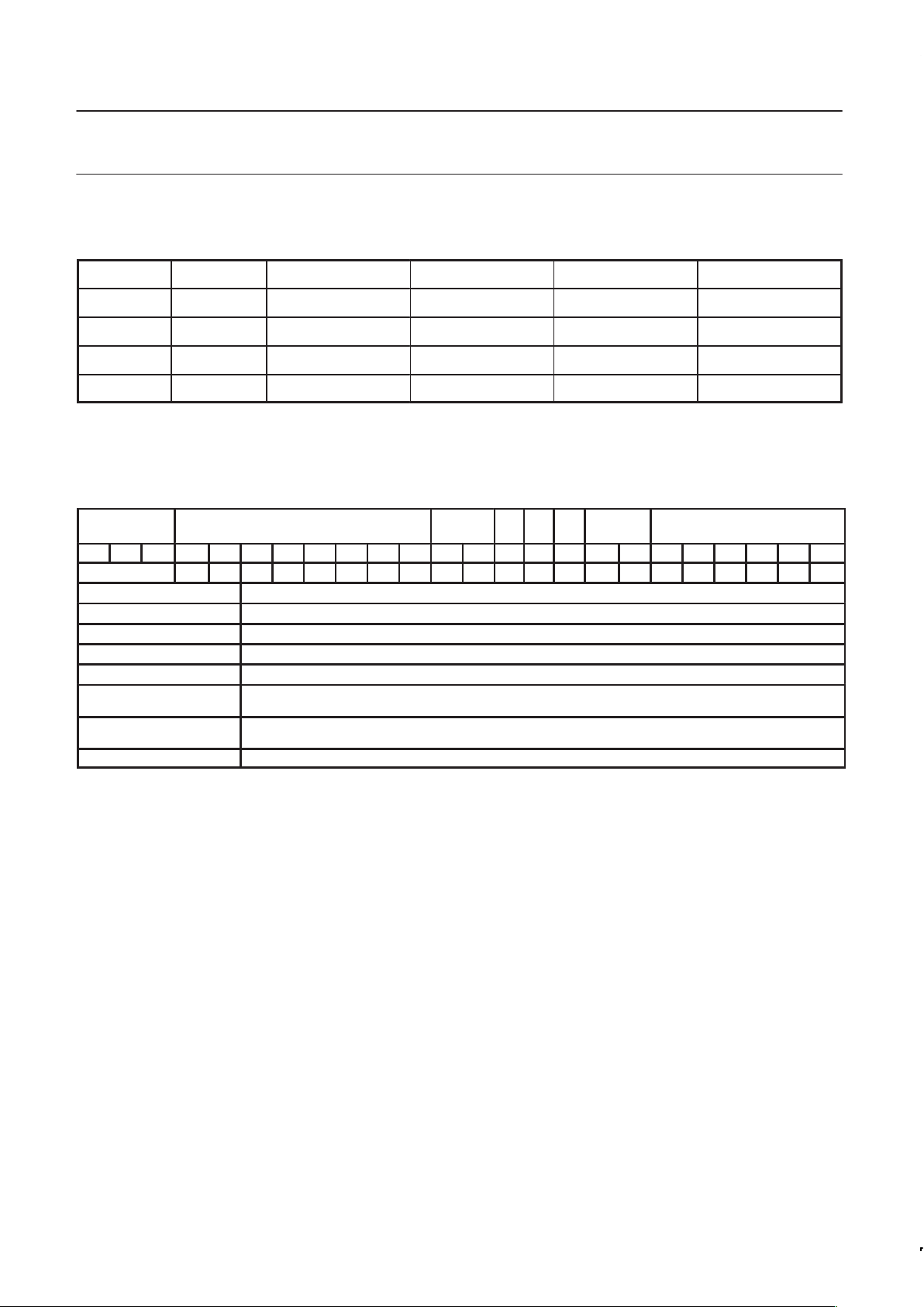
Main and auxiliary chargepump currents
CP1
CP0 I
PHA
I
PHP
I
PHP–SU
I
PHI_SU
0 0 1.5xlset 3xIset 15xlset 36xlset
0 1 0.5xlset 1xlset 5xlset 12xlset
1 0 1.5xlset 3xlset 15xlset 0
1 1 0.5xlset 1xlset 5xlset 0
NOTES
1. I
SET
= Vset/RN; bias current for charge pumps.
2. CP1 is used to disable the PHI pump.
3. Iphp_su is the total current out of PHP in speedup mode.
D word, length 24 bits
Address Power Control
M
divider
SE TM AD
Sleep
Mode
Test pa_current
1 1 0 PC7 PC6 PC5 PC4 PC3 PC2 PC1 PC0 M1 M0 SE TM AD SM1 SM2 pai5 pai4 pai3 pai2 pai1 pai0
Default: x x x x x x x x 0 0 0 0 0 0 0 0 0 0 0 0 0
D0 word select Fixed to 110.
Output Power Control PC7(msb)...PC0(Isb) Provides output power attenuation for DUAL mode amplifier outputs in 0.18 dB steps, Fx = 45.9 dB.
M Divider 00 = 6, 01 = 7, 10 = 8, 11 = 9
Offset loop power down SE Offset loop synthesizer power down, SE = 1 power on, SE = 0 power down (sleep mode).
DUAL mode select TM = 0 DUALmode
AMPS/DAMPS mode select AD = 1 DAMPS mode.
AD = 0 AMPs mode
TX buffers power down SM1 TX Local oscillator buffers power down. SM1 = 1 power on, SM1 = 0 to power down.
SM2 RCLK buffer power down. SM2 = 1 power on, SM2 = 0 to power down.
Test: pa_current:pai TX test bits for controlling the current in the power amp. Should be 0 during normal operation.
Page 17
Philips Semiconductors Objective specification
SA9025
900 MHz transmit modulator and 2.2 GHz
fractional–N synthesizer
1997 Aug 01
17
MODES OF OPERATION
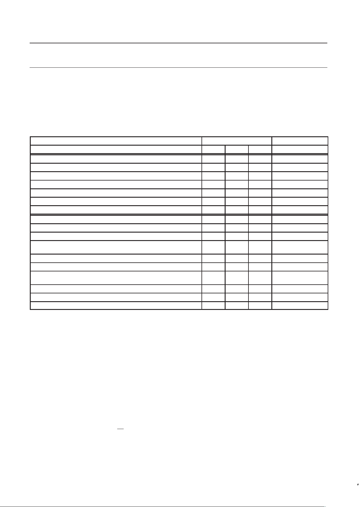
There are two power saving modes of operation which the circuit
can be put into, dependent on the status of the system. The
intention of these different modes is to disable circuitry that is not in
use at the time in order to reduce power consumption. During sleep
mode, only circuitry which is required to provide a master clock to
the digital portion of the system is enabled. During receive mode,
circuitry which is used to perform the receive function and provide a
master clock is enabled. In transmit mode all the functions of the
circuit are enabled which are required to perform transmit, receive
and provide master clock. When the circuit is powered for the first
time, it is in DUAL MODE SLEEP.
Mode Programming
Mode Dual Mode AMPS
Mode Setting and BlockStatus (X = ON) Sleep RX TX Logic
TX
EN
0 0 1
PD1 0 1 1
PD2 0 1 1
SE–>SYNen 0 0 1
TM 0 0 0
SM1 0 0 1
SM2 0 1 1
Main loop, Ndivider, RXLO buffer X X PD1
Aux loop, Adivider X X PD2
Rdivider X X PD1 .OR. PD2
Offset VCO, Mdivider X SE (+delay) See
SE–>SYN
EN
diagram
RCL buffer X X SM2
MCL buffer, reference input X X X 1 (always ON)
DUALTX PA X (.not. TM) .and. TX
EN
.and. SM1
TXLO buffer, SSB up–converter X SM1
I/Q MODULATOR, VGA X TXEN .AND. SM1
Control Logic X X X 1 (always ON)
Main Divider
The input signal on RXLO is amplified to a logic level by a balanced
input comparator giving a common mode rejection. This input stage
is enabled by serial control bit PD1 = 1. Disabling means that all
currents in the comparator are switched off. The main divider is built
up to be a 16-bit counter.
The loading of the work registers FMOD, NF and NMAIN is
synchronized with the state of the main counter to avoid extra phase
disturbance when switching over to another main divider ratio as is
explained in the Serial Programming Input chapter.
At the completion of a main divider cycle, a main divider output
pulse is generated which will drive the main phase comparator.
Also, the fractional accumulator is incremented with NF. The
accumulator works modulo Q. Q is preset by the serial control bit
FMOD to 8 when FMOD = ‘0’. Each time the accumulator
overflows, the total divide ratio will be NMAIN + 1 for the next cycle.
The mean division ratio over Q main divider cycles will then be:
NQ + NMAIN )
NF
Q
Synchronization is provided to avoid a random phase on the phase
detector upon the loading of a new ratio and when powering up the
loop.
Auxiliary Divider
The input signal on INA is amplified to logic level by a single-ended
input buffer, which accepts low level AC-coupled input signals. This
input stage is enabled if the serial control bit PD2 = ‘1’. Disabling
means that all currents in the buffer and prescaler are switched off.
The auxiliary divider is programmed with 14 bits and has continuous
integer division ratios over the range of 128 to 16,384.
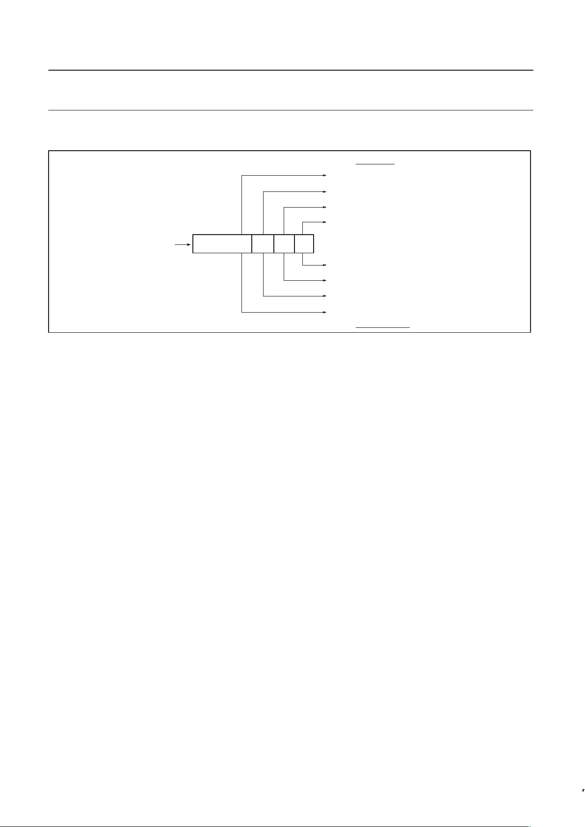
Reference Divider (Figure 8)
The input can be driven by a differential crystal input or an external
TCXO. This input stage is enabled by the OR function of the serial
input bits PD1 and PD2. Disabling means that all currents are
switched off. The reference divider consists of a programmable
divide by N
REF
(N
REF
= 4 to 1,023) followed by a 3-bit binary
counter. The 2 bit SM determines which of the four output pulses is
selected as the main phase detector signal. To obtain the best time
spacing for the main and auxiliary reference signals, a different
output will be used for the auxiliary phase detector, reducing the
possibility of unwanted interactions.
Page 18
Philips Semiconductors Objective specification
SA9025
900 MHz transmit modulator and 2.2 GHz
fractional–N synthesizer
1997 Aug 01
18
SR01440
RSA = “11”
RSA = “10”
RSA = “01”
RSA = “00”
RSM = “11”
RSM = “10”
RSM = “01”
RSM = “00”
MAIN SELECT
AUXILIARY SELECT
REFERENCE
INPUT
DIVIDE BY NREF /2 /2 /2
Figure 8. Reference Variable Divider
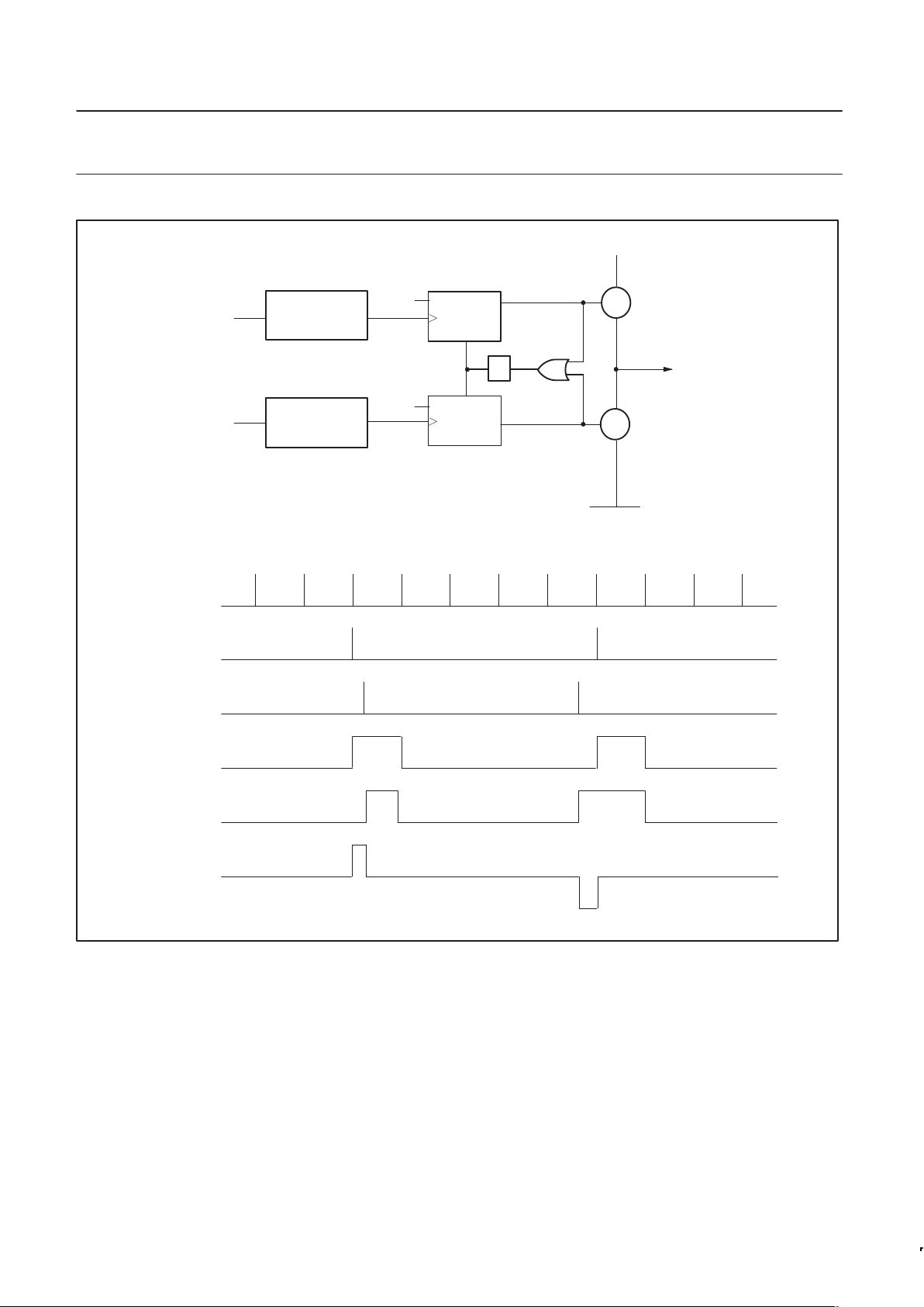
Phase Detectors (Figure 9)
The auxiliary and main phase detectors each consist of a 2 D-type
flip-flop phase and frequency detector. Each flip-flop is set by the
negative edge of the divider terminal count output pulse. The reset
inputs are activated after a delay when both flip-flops have been set.
This avoids non-linearity or dead-band around zero phase error.
The flip-flops drive on-chip charge pumps. A pull-up current from
the charge pump indicates the VCO frequency shall be increased
while a pull-down pulse indicates the VCO frequency shall be
decreased.
Current Settings
The IC has two current setting pins, RN and I
PEAK
. The active
charge pump currents and the fractional compensation currents are
linearly dependent on the current in the current setting pins. This
current, I
SET
, is set by an external resistor connected between the
current setting pin and V
SS
.
Auxiliary Output Charge Pumps
The auxiliary charge pumps on pin PHA are driven by the auxiliary
phase detector and the current value is determined by the external
resistor attached to pin RN.
Page 19
Philips Semiconductors Objective specification
SA9025
900 MHz transmit modulator and 2.2 GHz
fractional–N synthesizer
1997 Aug 01
19
SR01451
R
X
P
N
REF DIVIDER
AUX/MAIN
DIVIDER
D
Q
CLK
“1”
R
D
R
CLK
“1”
X
Q
N
P
τ
V
DDA
GND
PH
V
SSA
P–TYPE
CHARGE PUMP
N–TYPE
CHARGE PUMP
R
INR
INR
I
PH
Figure 9. Phase Detector Structure With Timing
Main Output Charge Pumps and Fractional
Compensation Currents
The main charge pumps on pin PHP and PHI are driven by the main
phase detector. The current value is determined by the current at
pin RN. The fractional compensation current is linearly dependent
on the main charge pump current and its level relative to the main
charge pumps is set by an 8-bit programmable DAC. The timing for
the fractional compensation is derived from the main divider. The
current level based on the value of FRD, FDAC and I
SET
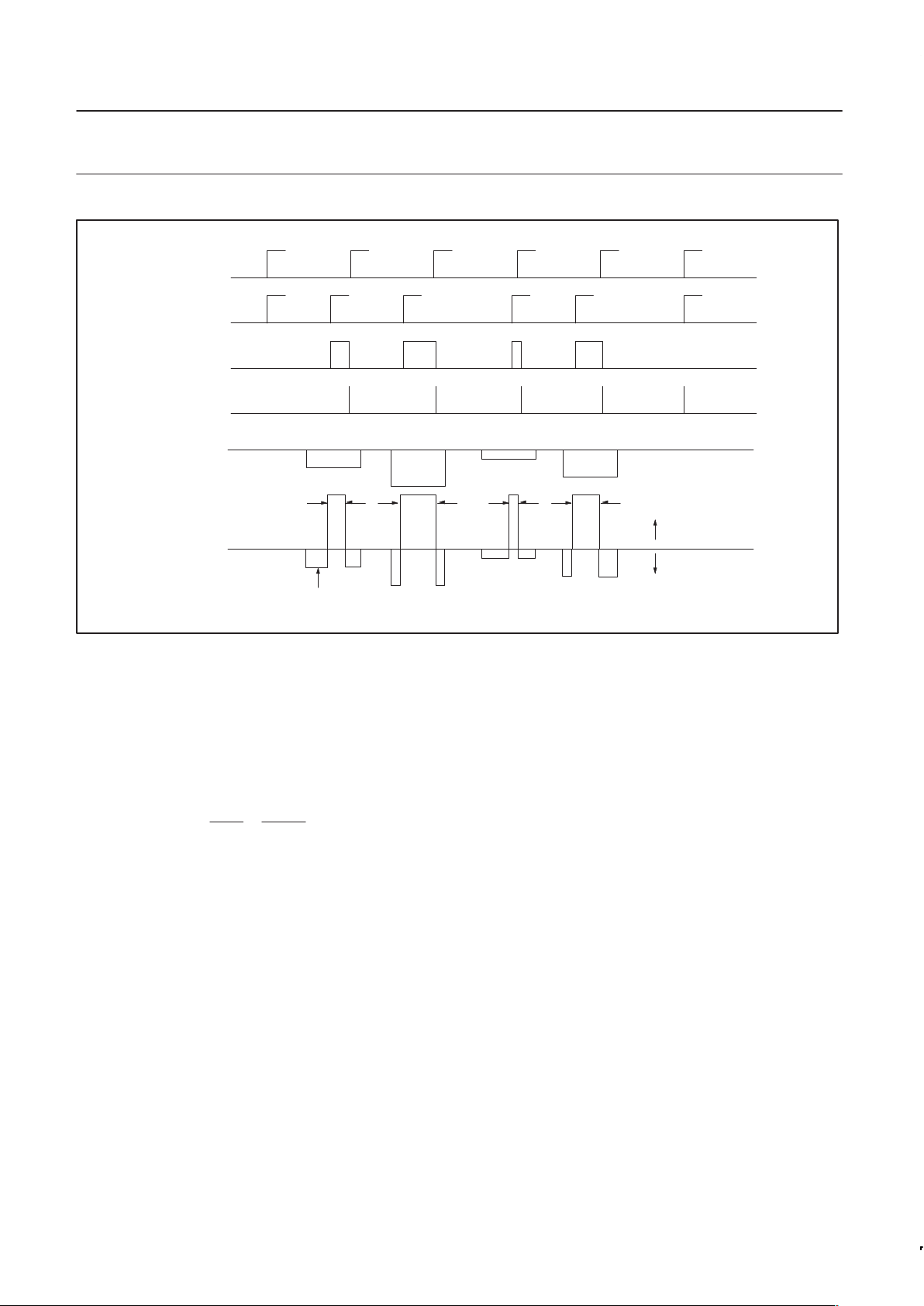
. Figure 10
shows the waveforms (not to scale) for a typical base.
Page 20
Philips Semiconductors Objective specification
SA9025
900 MHz transmit modulator and 2.2 GHz
fractional–N synthesizer
1997 Aug 01
20
SR01454
REFERENCE R
MAIN M
VCO CYCLES
N N N+1 N N+1
DETECTOR
OUTPUT
ACCUMULATOR
241
3
0
FRACTIONAL
COMPENSATION
CURRENT
OUTPUT ON
PHP, PHI
PULSE
WIDTH
MODULATION
PULSE LEVEL
MODULATION
mA
µA
CONTENTS
Figure 10. Waveforms for NF = 2; Fraction = 0.4
Figure 10 shows that for a proper fractional compensation, the area
of the fractional compensation current pulse must be equal to the
area of the charge pump ripple output.
The fractional compensation current is derived from the main charge
pump in that it will follow all the current scaling through external
resistor setting, programming or speedup operation.
For a given pump,
|comp +
|pump
128
x
Fdac
5 x 128
xFRD
Where:
Icomp is the compensation current, Ipump is the pump current, Fdac
is the fractional DAC value and FRD is the fractional accumulator
value.
The theoretical value for Fdac would then be: 128 for Fmod = 1
(modulo 5) and 80 for Fmod = 0 (modulo 8).
When the serial input A word is loaded, the output circuits are in the
“speedup mode” as long as the STROBE is H, otherwise the
“normal mode” is active.
Lock Detect
The output LOCK maintains a logic ‘1’ when the auxiliary phase
detector ANDed with the main phase detector indicates a lock
condition. The lock condition for the main and auxiliary synthesizers
is defined as a phase difference of less than "1 cycle on the
reference inputs XTAL1,2. The LOCK condition is also fulfilled when
the relative counter is disabled (PD
main
= ‘0’ or PD
aux
= ‘0’) for the
main or auxiliary counter, respectively. Lock indication when PD
main
= PD
aux
= ‘0’.
Functional Description of Offset Loop, Modulator
and Power Control
Transmit Offset Synthesizer
The transmit offset phase locked loop portion of the SA9025 design
consists of the following functional blocks: reference oscillator,
limiters, phase detector, ÷M, IF VCO and passive loop filter.
Harmonic contents of this signal are attenuated by an LP filter. The
output of the IF VCO is also divided by N and compared with the
reference oscillator in the phase detector.
Reference Oscillator
This Oscillator is used to generate the reference frequency together
with an external crystal and varicap. The output is internally routed
to three buffers and a phase comparator . It is possible to run the
oscillator as an amplifier from an external reference signal (TCXO).
Phase Detector and Charge Pump
The phase comparator is used to compare the output of the divider
with the reference. It provides an output proportional to the phase
difference between the divided down VCO and the reference. This
output is then filtered and used as the control voltage input to the
VCO. The phase detector is a Gilbert multiplier cell type, having a
linear output from 0 to π (π/2 ±π/2), followed by a charge pump. The
charge pump peak output current is programmable to 6.4mA via the
use of an external resistor.
A preliminary design analysis has been performed with the following
loop parameters:
A lock detect signal is provided and ANDed together with lock detect
signals from both the main channel synthesizer and auxiliary
Page 21
Philips Semiconductors Objective specification
SA9025
900 MHz transmit modulator and 2.2 GHz
fractional–N synthesizer
1997 Aug 01
21
synthesizer. While in standby mode, the lock detect signal will be
forced to a valid lock state so that the lock detect signal will indicate
when the main and auxiliary phase detectors have achieved phase
lock.
Divide by M
The ÷M is a 2-bit programmable divider which can be configured for
ney integer divide from 6 to 9. The divider is used to convert the
VCO output down to the reference frequency before feeding it into
the phase comparator.
VCO
This oscillator is used to generate the transmit IF frequency between
90MHz and 180MHz. The VCO tank is configured using a parallel
inductor tuning varactor diode. DC blocking capacitors are used to
isolate the varactor control voltage from the VCO tank DC bias
voltages.
SSB Up-converter and TXIF Buffer
The TXIF buffer provides isolation between the SSB Up-converter
and the VCO output. The Single Sideband Up-converter (SSB) is
an active Gilbert cell multiplier (matched pair), combined with two
quadrature phase shift networks and a low pass filter. The SSB
up-converter is used to reject the unwanted upper sideband that
would normally occur during the up-conversion process.
I/Q Modulator
The quadrature modulator is an active Gilbert cell multiplier
(matched pair) with cross coupled outputs. These outputs are then
provided to the variable gain amplifier. When the in-phase input I =
cos (ωt) and the quadrature-phase input Q = sin (ωt) (i.e., Q lags I
by 90°), the resulting output should be upper single sideband.
Variable Gain Amplifiers
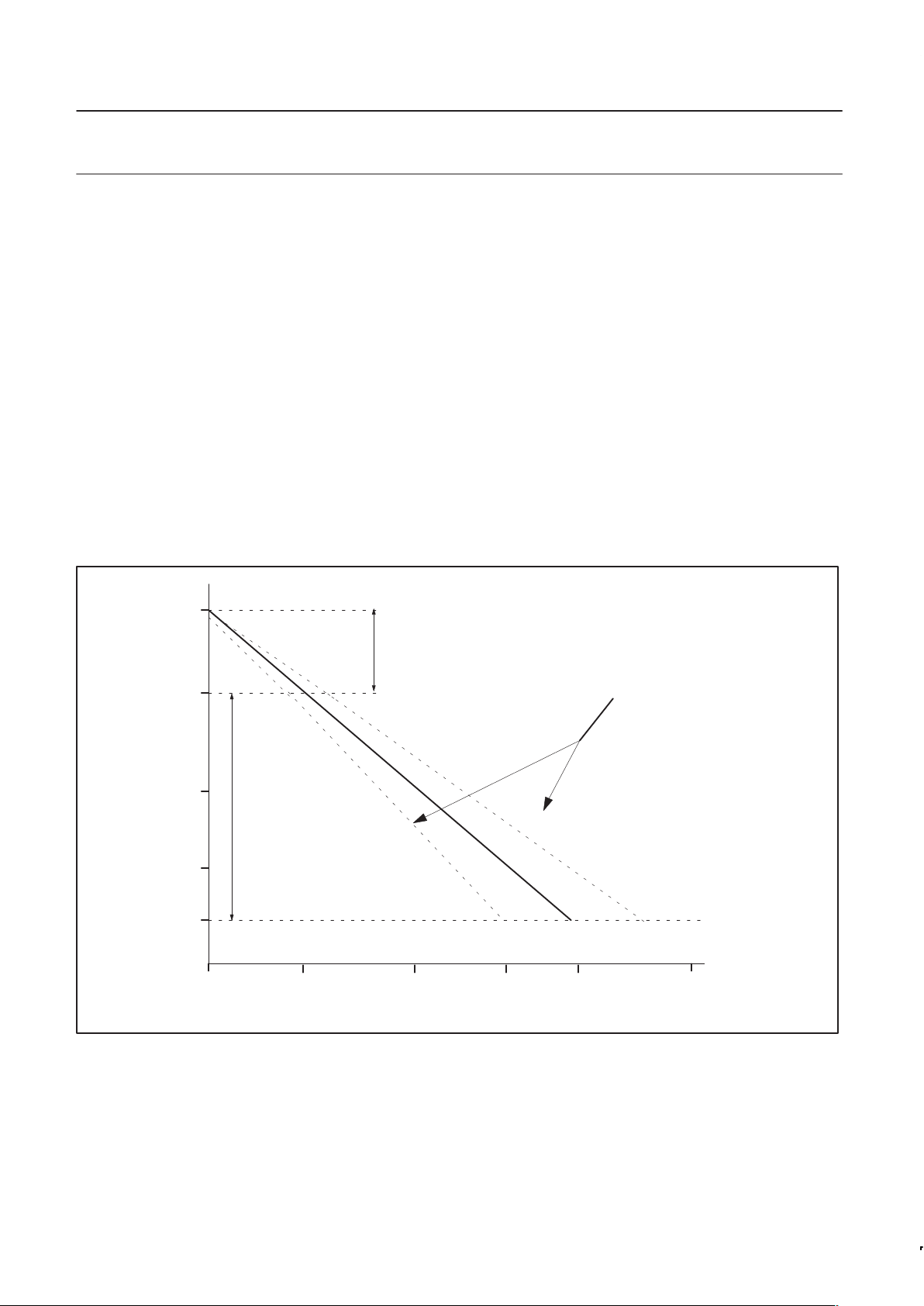
The variable gain amplifiers are used to control the output level of
the device, with a power control range of 45.9dB. The output stages
are differential, matched from 200Ω to 50Ω .
Power Control
The power control range should be greater than or equal to 45.9dB,
having a monotonically decreasing slope, with 0dB = +11.5 dBm
nominal. Eight bits are available for power control programming.
The top 6 bits (PC7 to PC2) provide coarse attenuation with .6dB
step size accuracy. The bottom 2 bits provide fine attenuation with
.18 dB step size accuracy.
SR01453
MAXIMUM ACCUMULATED ERROR
(NOT TO SCALE)
TOP 12 dB FINE STEP ACURACY
BOTTOM 25 dB COARSE STEP AC-
CURACY
+11.5
–3
–15
–26
–28
0 12 24 38 45.9
VGA SETTING (dB)
POWER OUT (dBm nom)
Figure 11. Power Control
Oscillator Buffers
There are three buffers for the reference signal, two of which are
used to provide external reference signals. The internal reference
signal is used for the main and auxiliary synthesizer reference. The
second buffer (MCLK) is used as a master clock for external digital
circuitry which is always on, while the third buffer (RCLK) is used as
a clock for external digital circuitry which is not used in sleep mode.
LO Buffers
The LO buffers are used to provide isolation for the VCO and
between the transmitter up-converter and channel synthesizer.
Page 22
900 MHz transmit modulator and 2.2 GHz
fractional–N synthesizer
Philips Semiconductors Objective specification
SA9025
1997 Aug 01
22
LQFP48: plastic low profile quad flat package; 48 leads; body 7 x 7 x 1.4 mm SOT313-2
Page 23
900 MHz transmit modulator and 2.2 GHz
fractional–N synthesizer
Philips Semiconductors Objective specification
SA9025
1997 Aug 01
23
Philips Semiconductors and Philips Electronics North America Corporation reserve the right to make changes, without notice, in the products,
including circuits, standard cells, and/or software, described or contained herein in order to improve design and/or performance. Philips
Semiconductors assumes no responsibility or liability for the use of any of these products, conveys no license or title under any patent, copyright,
or mask work right to these products, and makes no representations or warranties that these products are free from patent, copyright, or mask
work right infringement, unless otherwise specified. Applications that are described herein for any of these products are for illustrative purposes
only. Philips Semiconductors makes no representation or warranty that such applications will be suitable for the specified use without further testing
or modification.
LIFE SUPPORT APPLICA TIONS
Philips Semiconductors and Philips Electronics North America Corporation Products are not designed for use in life support appliances, devices,
or systems where malfunction of a Philips Semiconductors and Philips Electronics North America Corporation Product can reasonably be expected
to result in a personal injury. Philips Semiconductors and Philips Electronics North America Corporation customers using or selling Philips
Semiconductors and Philips Electronics North America Corporation Products for use in such applications do so at their own risk and agree to fully
indemnify Philips Semiconductors and Philips Electronics North America Corporation for any damages resulting from such improper use or sale.
This data sheet contains preliminary data, and supplementary data will be published at a later date. Philips
Semiconductors reserves the right to make changes at any time without notice in order to improve design
and supply the best possible product.
Philips Semiconductors
811 East Arques Avenue
P.O. Box 3409
Sunnyvale, California 94088–3409
Telephone 800-234-7381
DEFINITIONS
Data Sheet Identification Product Status Definition
Objective Specification
Preliminary Specification
Product Specification
Formative or in Design
Preproduction Product
Full Production
This data sheet contains the design target or goal specifications for product development. Specifications
may change in any manner without notice.
This data sheet contains Final Specifications. Philips Semiconductors reserves the right to make changes
at any time without notice, in order to improve design and supply the best possible product.
Philips Semiconductors and Philips Electronics North America Corporation
register eligible circuits under the Semiconductor Chip Protection Act.
Copyright Philips Electronics North America Corporation 1997
All rights reserved. Printed in U.S.A.
print code Date of release: 05-96
Document order number:
 Loading...