

Page 1

SA8025A
Low-voltage 1.8GHz fractional-N
synthesizer
Product specification 1996 Oct 15
INTEGRATED CIRCUITS
IC17 Data Handbook
Page 2
Philips Semiconductors Product specification
SA8025A1.8GHz low-voltage Fractional-N synthesizer
2
1996 Oct 15 853-1785 17401
DESCRIPTION
The SA8025A is a monolithic low power, high performance dual
frequency synthesizer fabricated in QUBiC BiCMOS technology.
The SA8025A is an improved version of the SA8025, suitable for
narrow band systems like the Japan Personal Digital Cellular (PDC)
system. The new design improves the performance of the fractional
spur compensation circuitry. The new version is pin-for-pin
compatible with the previous version. Featuring Fractional-N
division with selectable modulo 5 or 8 implemented in the Main
synthesizer to allow the phase detector comparison frequency to be
five or eight times the channel spacing. This feature reduces the
overall division ratio yielding a lower noise floor and faster channel
switching. The phase detectors and charge pumps are designed to
achieve phase detector comparison frequencies up to 5MHz. A four
modulus prescaler (divide by 64/65/68/73) is integrated on chip with
a maximum input frequency of 1.8GHz at 3V . Programming and
channel selection are realized by a high speed 3-wire serial
interface. A 1GHz version (SA7025DK) is also available with the
same pinout.
FEATURES
•Operation up to 1.8GHz at 3V
•Fast locking by “Fractional-N” divider
•Auxiliary synthesizer
•Digital phase comparator with proportional and integral charge
pump output
•High speed serial input
•Low power consumption
•Programmable charge pump currents
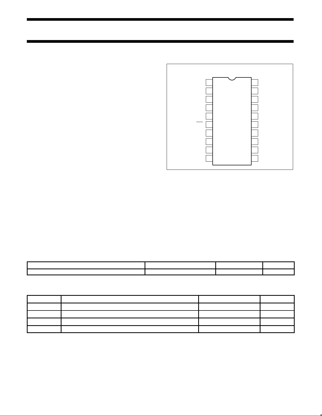
PIN CONFIGURATION
V
SS
DATA
CLOCK
DK Package
1
2
3
4
5
6
7
8
9
10
11
12
13
14
20
19
18
17
16
15
STROBE
RA
TEST
V
DD
RF
RN
PHA
V
DDA
PHP
V
SSA
PHI
LOCK
RF
IN
RF
IN
V
CCP
REF
IN
AUX
IN
SR00623
Figure 1. Pin Configuration
•Supply voltage range 2.7 to 5.5V
•Excellent input sensitivity: V
RF_IN
= –20dBm
APPLICATIONS
•PHS (Personal Handy-phone System)
•PDC (Personal Digital Cellular)
•PCS (Personal Communication Service)
•Portable communication systems
ORDERING INFORMATION
DESCRIPTION TEMPERATURE RANGE ORDER CODE DWG #
20-Pin Plastic Shrink Small Outline Package (SSOP) –40 to +85°C SA8025ADK SOT266-1
ABSOLUTE MAXIMUM RATINGS
SYMBOL PARAMETER RATING UNITS
V Supply voltage, VDD, V
DDA
, V
CCP
-0.3 to +6.0 V
V
IN
Voltage applied to any other pin -0.3 to (VDD + 0.3) V
T
STG
Storage temperature range -65 to +150 °C
T
A
Operating ambient temperature range -40 to +85 °C
NOTE: Thermal impedance (θJA) = 117°C/W. This device is ESD sensitive.
Page 3
Philips Semiconductors Product specification
SA8025A1.8GHz low-voltage Fractional-N synthesizer
1996 Oct 15
3
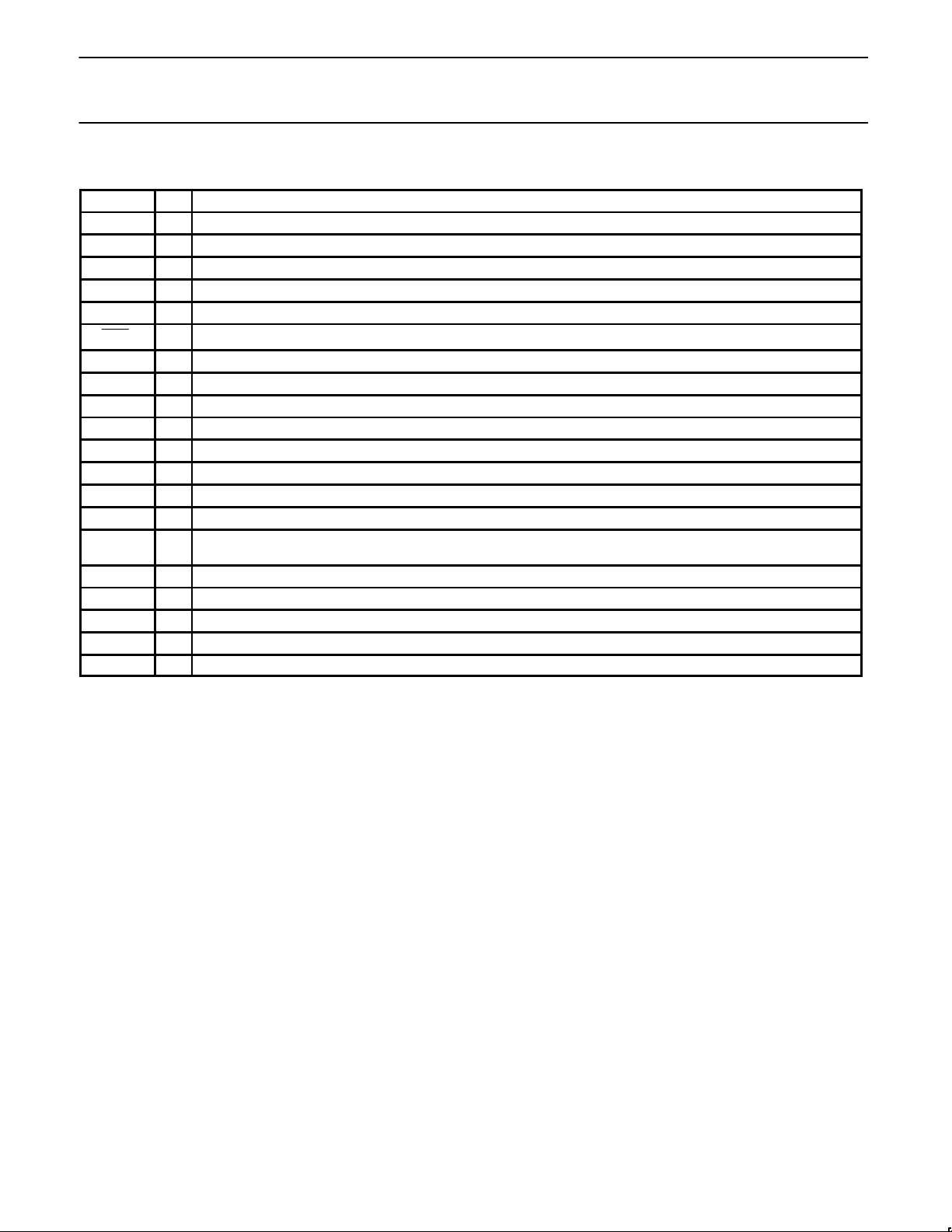
PIN DESCRIPTIONS
Symbol Pin Description
CLOCK 1 Serial clock input
DATA 2 Serial data input
STROBE 3 Serial strobe input
V
SS
4 Digital ground
RF
IN
5 Prescaler positive input
RF
IN
6 Prescaler negative input
V
CCP
7 Prescaler positive supply voltage. This pin supplies power to the prescaler and RF input buffer
REF
IN
8 Reference divider input
RA 9 Auxiliary current setting; resistor to V
SSA
AUX
IN
10 Auxiliary divider input
PHA 11 Auxiliary phase detector output
V
SSA
12 Analog ground
PHI 13 Integral phase detector output
PHP 14 Proportional phase detector output
V
DDA
15 Analog supply voltage. This pin supplies power to the charge pumps, Auxiliary prescaler, Auxiliary and Reference
buffers.
RN 16 Main current setting; resistor to V
SSA
RF 17 Fractional compensation current setting; resistor to V
SSA
LOCK 18 Lock detector output
TEST 19 Test pin; connect to V
DD
V
DD
20 Digital supply voltage. This pin supplies power to the CMOS digital part of the device
Page 4
Philips Semiconductors Product specification
SA8025A1.8GHz low-voltage Fractional-N synthesizer
1996 Oct 15
4
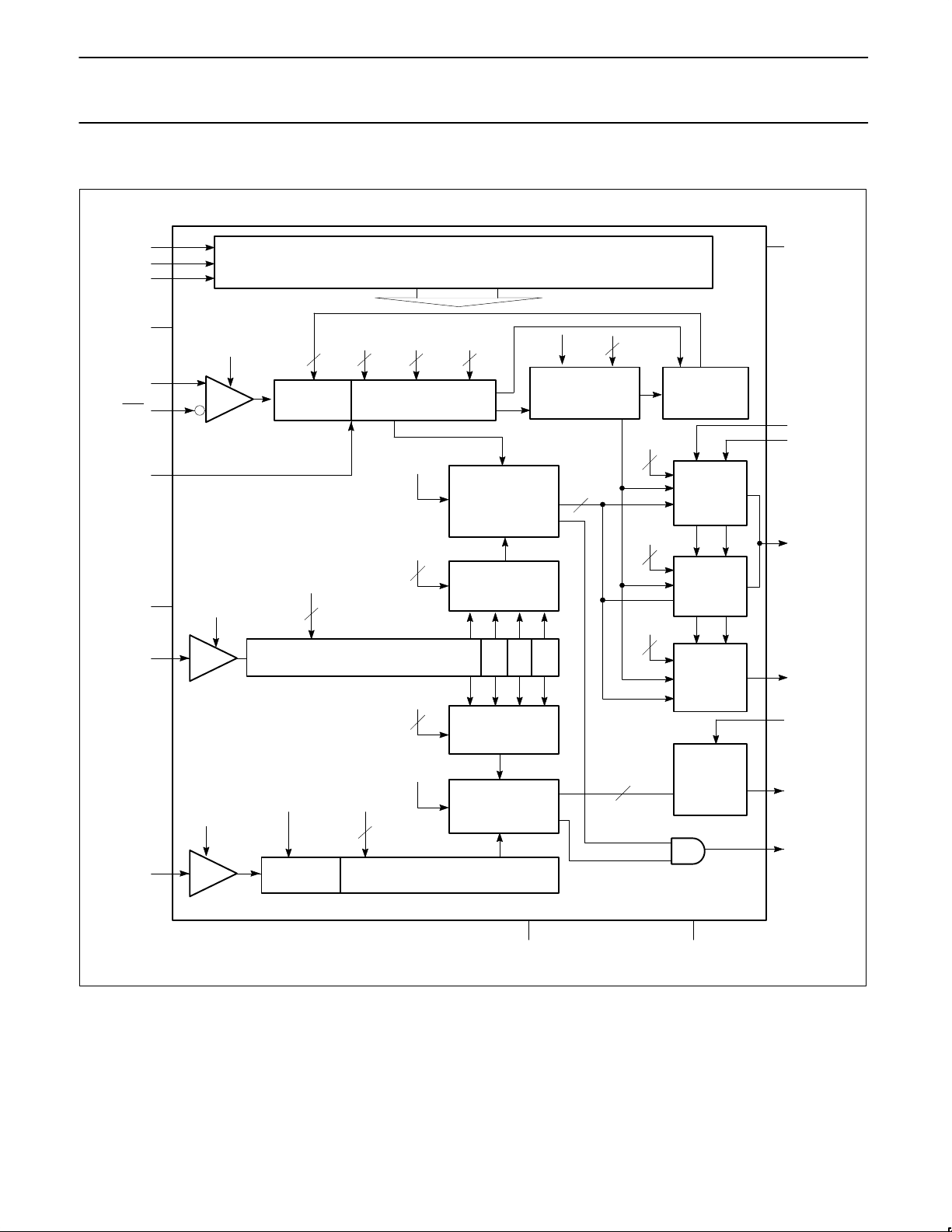
BLOCK DIAGRAM
SERIAL INPUT + PROGRAM LATCHES
MAIN DIVIDERS
PRESCALER
MODULUS
NORMAL
OUTPUT
CHARGE
PUMP
INTEGRAL
OUTPUT
CHARGE
PUMP
AUXILIARY
OUTPUT
CHARGE
PUMP
MAIN
PHASE
DETECTOR
MAIN
REFERENCE
SELECT
SPEED-UP
OUTPUT
CHARGE
PUMP
REFERENCE DIVIDER ÷2 ÷2 ÷2
AUXILIARY
REFERENCE
SELECT
AUXILIARY
PHASE
DETECTOR
AUXILIARY DIVIDER
1/4
DATA
CLOCK
STROBE
RF
IN
RF
IN
REF
IN
AUX
IN
FB
RF
RN
PHP
PHI
RA
PHA
LOCK
V
DD
V
DDA
V
SS
V
SSA
EM
PR NM1
NM2
NM3
FMOD
NF
2
12 8
3
FRD
CN
8
2
2
EM
NR
EM+EA
12
SA
EA
PA NA
2
4
SM
EA
2
CK
CL
2
12
FRACTIONAL
ACCUMULATOR
64/65/68/73
FB
TEST
V
CCP
PRESCALER
2
CONTROL
PRESCALER
SR00624
Figure 2. Block Diagram
Page 5
Philips Semiconductors Product specification
SA8025A1.8GHz low-voltage Fractional-N synthesizer
1996 Oct 15
5
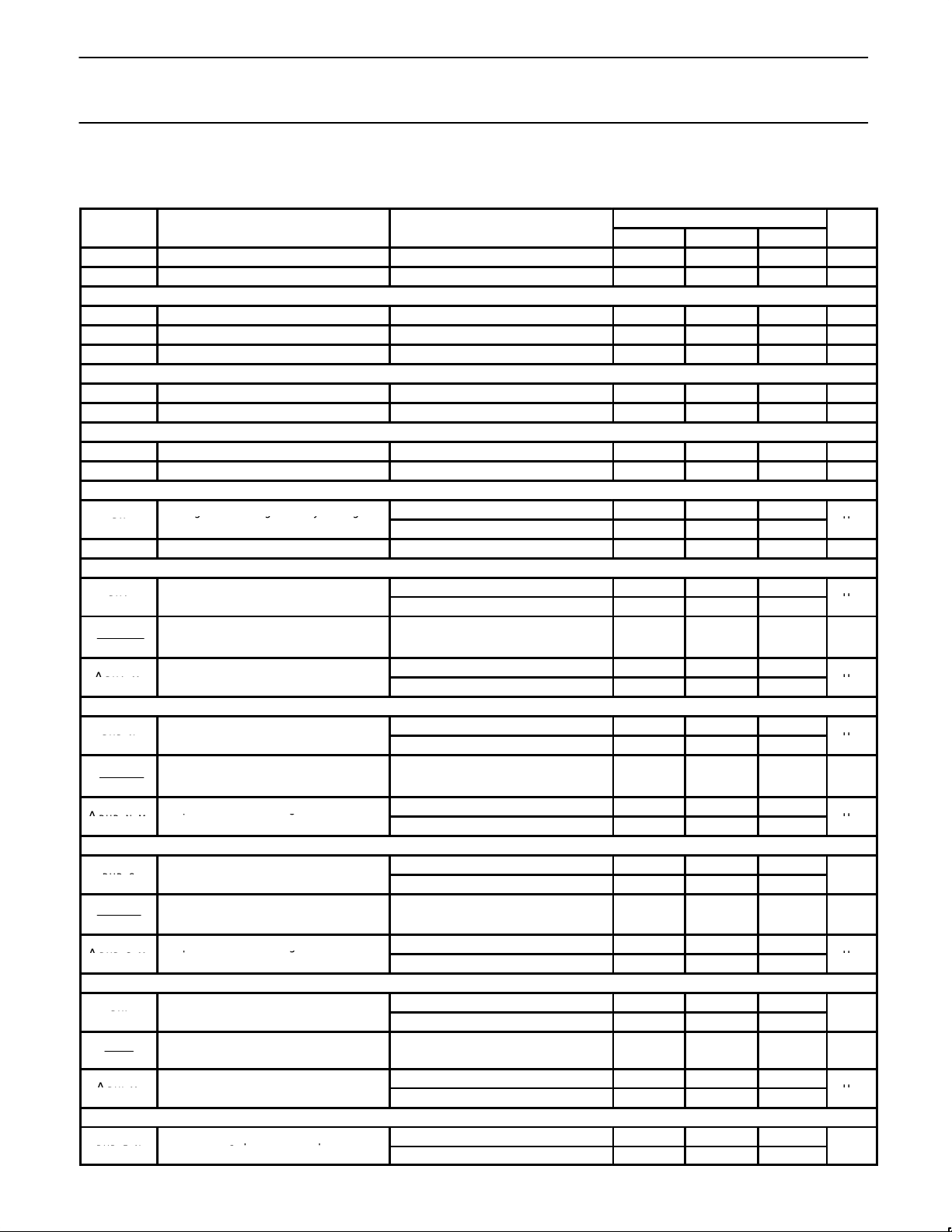
DC ELECTRICAL CHARACTERISTICS
VDD = V
DDA
= V
CCP
= 3V; TA = 25°C, unless otherwise specified.
LIMITS
SYMBOL
PARAMETER
TEST CONDITIONS
MIN TYP MAX
UNITS
V
SUPPLY
Recommended operating conditions V
CCP
= VDD, V
DDA
≥ V
DD
2.7 5.5 V
I
STANDBY
Total standby supply currents EM = EA = 0, IRN = IRF = IRA = 0 50 500 µA
Operational supply currents: I = IDD + I
CCP
+ I
DDA
; IRN = 25µA, IRA = 25µA, (see Note 5)
I
AUX
Operational supply currents EM = 0, EA = 1 3.5 mA
I
MAIN
Operational supply currents EM = 1, EA = 0 11.0 mA
I
TOTAL
Operational supply currents EM = EA = 1 13.5 mA
Digital inputs CLK, DATA, STROBE
V
IH
High level input voltage range 0.7xV
DD
V
DD
V
V
IL
Low level input voltage range 0 0.3xV
DD
V
Digital outputs LOCK
V
OL
Output voltage LOW IO = 2mA 0.4 V
V
OH
Output voltage HIGH IO = –2mA VDD–0.4 V
Charge pumps: V
DDA
= 3V / IRX = 25µA or V
DDA
= 5V / IRX = 62.5µA, V
PHX
in range, unless otherwise specified.
2.7V < V
DDA
< 5.5V 25
|IRX|
Setting current range for any setting re-
sistor
4.5V < V
DDA
< 5.5V 62.5
µA
V
PHOUT
Output voltage range 0.7 V
DDA
–0.8 V
Charge pump PHA
IRN = –62.5µA; V
PHP
= V
DDA
/2
13
400 500 600
|I
PHA
|
Output current PHA
IRN = –25µA; V
PHP
= V
DDA
/2 160 200 240
µA
I
PHP_A
| I
PHP_A
|
Relative output current variation PHA IRA = –62.5µA
2, 13
2 6 %
V
DDA
= 3V, IRA = 25µA ±50
∆I
PHA_M
Output current matching PHA pump
V
DDA
= 5V, IRA = 62.5µA ±65
µA
Charge pump PHP, normal mode
NO TAG, 4, 6
VRF = V
DDA
IRN = –62.5µA; V
PHP
= V
DDA
/2
13
440 550 660
|I
PHP_N
|
Output current PHP
IRN = –25µA; V
PHP
= V
DDA
/2 175 220 265
µA
I
PHP_N
I
PHP_N
Relative output current variation PHP IRN = –62.5µA
2, 13
2 6 %
V
DDA
= 3V, IRA = 25µA ±50
∆I
PHP_N_M
Output current matching PHP
normal mode
V
DDA
= 5V, IRA = 62.5µA ±65
µA
Charge pump PHP, speed-up mode
NO TAG, 4, 7
VRF = V
DDA
IRN = –62.5µA; V
PHP
= V
DDA
/2
13
2.20 2.75 3.30
|I
PHP_S
|
Output current PHP
IRN = –25µA; V
PHP
= V
DDA
/2 0.85 1.1 1.35
mA
I
PHP_S
I
PHP_S
Relative output current variation PHP IRN = –62.5µA
2, 13
2 6 %
V
DDA
= 3V, IRA = 25µA ±250
∆I
PHP_S_M
Output current matching PHP
speed-up mode
V
DDA
= 5V, IRA = 62.5µA ±300
µA
Charge pump PHI, speed-up mode
NO TAG, 4, 8
VRF = V
DDA
IRN = –62.5µA; V
PHI
= V
DDA
/2
13
4.4 5.5 6.6
|I
PHI
|
Output current PHI
IRN = –25µA; V
PHI
= V
DDA
/2 1.75 2.2 2.65
mA
I
PHI
I
PHI
Relative output current variation PHI IRN = –62.5µA
2, 13
2 8 %
V
DDA
= 3V, IRA = 25µA ±500
∆I
PHI_M
Output current matching PHI pump
V
DDA
= 5V, IRA = 62.5µA ±600
µA
Fractional compensation PHP, normal mode
NO TAG, 9
V
RN
= V
DDA
, V
PHP
= V
DDA
/2
IRF = –62.5µA;FRD = 1 to 7
13
–625 –400 –250
I
PHP_F_N
Fractional compensation output current
PHP vs F
RD
3
IRF = –25µA;FRD = 1 to 7 –300 –180 –50
nA
Setting current range for any setting re-
Output current matching PHP
Output current matching PHP
Fractional compensation output current
Page 6
Philips Semiconductors Product specification
SA8025A1.8GHz low-voltage Fractional-N synthesizer
1996 Oct 15
6
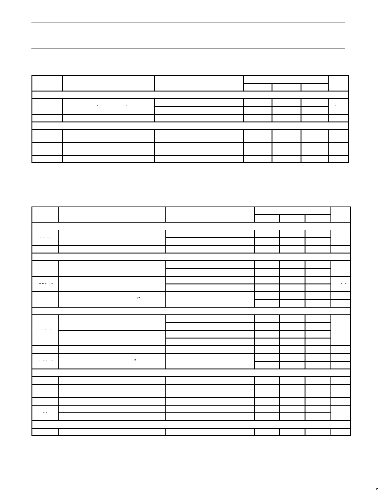
DC ELECTRICAL CHARACTERISTICS (Continued)
LIMITS
SYMBOL
PARAMETER
TEST CONDITIONS
MIN TYP MAX
UNITS
Fractional compensation PHP, speed up mode
NO TAG, 10
V
PHP
= V
DDA
, VRN = V
DDA
IRF = –62.5µA;FRD = 1 to 7
13
–3.35 –2 –1.1
I
PHP_F_S
Fractional compensation output current
PHP vs F
RD
3
IRF = –25µA;FRD = 1 to 7 –1.35 –1.0 –0.5
µA
Pump leakage –20 20 nA
Charge pump leakage currents, charge pump not active
I
PHP_L
Output leakage current PHP; normal
mode
NO TAG
V
PHP
= 0.7 to V
DDA
– 0.8 0.1 20 nA
I
PHI_L
Output leakage current PHI; normal
mode
NO TAG
V
PHI
= 0.7 to V
DDA
– 0.8 0.1 20 nA
I
PHA_L
Output leakage current PHA V
PHA
= 0.7 to V
DDA
– 0.8 0.1 20 nA
AC ELECTRICAL CHARACTERISTICS
VDD = V
DDA
= V
CCP
= 3V; TA = 25°C; unless otherwise specified. Test Circuit, Figure 4. The parameters listed below are tested using
automatic test equipment to assure consistent electrical characteristics. The limits do not represent the ultimate performance limits of the
device. Use of an optimized RF layout will improve many of the listed parameters.
LIMITS
SYMBOL
PARAMETER
TEST CONDITIONS
MIN TYP MAX
UNITS
Main divider guaranteed and tested on an automatic tester. Some performance parameters may be improved by using optimized layout.
Pin = -20dBm, Direct coupled input
14
0 1.8
f
RF_IN
Input signal frequency
Pin = -20dBm, 1000pF input coupling 1.8
GHz
V
RF_IN
Input sensitivity fIN = 1800MHz –20 0 dBm
Reference divider (VDD = V
DDA
= 3V or VDD = 3V / V
DDA
= 5V)
2.7 < VDD and V
DDA
< 5.5V 25
f
REF_IN
Input signal frequency
2.7 < VDD and V
DDA
< 4.5V 30
MHz
2.7 < VDD and V
DDA
< 5.5V 500
V
REF_IN
Input signal range, AC coupled
2.7 < VDD and V
DDA
< 4.5V 300
mV
P-P
100 kΩ
Z
REF_IN
Reference divider input impedance
15
3 pF
Auxiliary divider
Input signal frequency 0 50
PA = “0”, prescaler enabled 4.5V ≤ V
DDA
≤ 5.5V 0 150
f
AUX_IN
Input signal frequency 0 30
MHz
PA = “1”, prescaler disabled 4.5V ≤ V
DDA
≤ 5.5V 0 40
V
AUX_IN
Input signal range, AC coupled 200 mV
P-P
100 kΩ
Z
AUX_IN
Auxiliary divider input impedance
15
3 pF
Serial interface
15
f
CLOCK
Clock frequency 10 MHz
t
SU
Set-up time: DATA to CLOCK,
CLOCK to STROBE
30 ns
t
H
Hold time; CLOCK to DATA 30 ns
Pulse width; CLOCK 30
t
W
Pulse width; STROBE B, C, D, E words 30
ns
In-Loop Performance16 V
DDA
= 5V, VDD = 2.7V
RF
MM
Main loop residual FM F
VCO
= 1780MHz 600 900 Hz
Fractional compensation output current
Page 7
Philips Semiconductors Product specification
SA8025A1.8GHz low-voltage Fractional-N synthesizer
1996 Oct 15
7
AC ELECTRICAL CHARACTERISTICS (Continued)
LIMITS
SYMBOL
PARAMETER
TEST CONDITIONS
MIN TYP MAX
UNITS
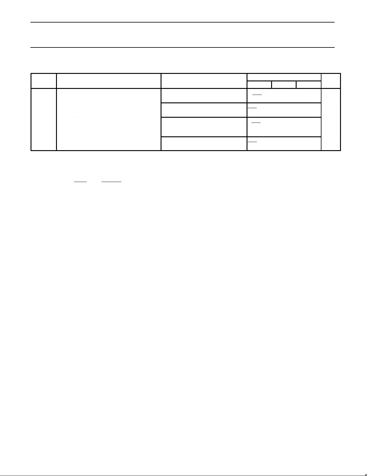
A word, PR = ‘01’
(NM2 65) t
W
A word, PR = ‘10’
1
f
VCO
[(NM2 65) (NM3 1) 68] t
W
A word, PR = ‘11’
[(NM2 65 (NM3 1) 68
(NM4 1) 73)] t
W
A word, PR = ‘00’
[(NM2 65) (NM4 1) 73] t
W
NOTES:
1. When a serial input “A” word is programmed, the main charge pumps on PHP and PHI are in the “speed up mode” as long as STROBE = H.
When this is not the case, the main charge pumps are in the “normal mode”.
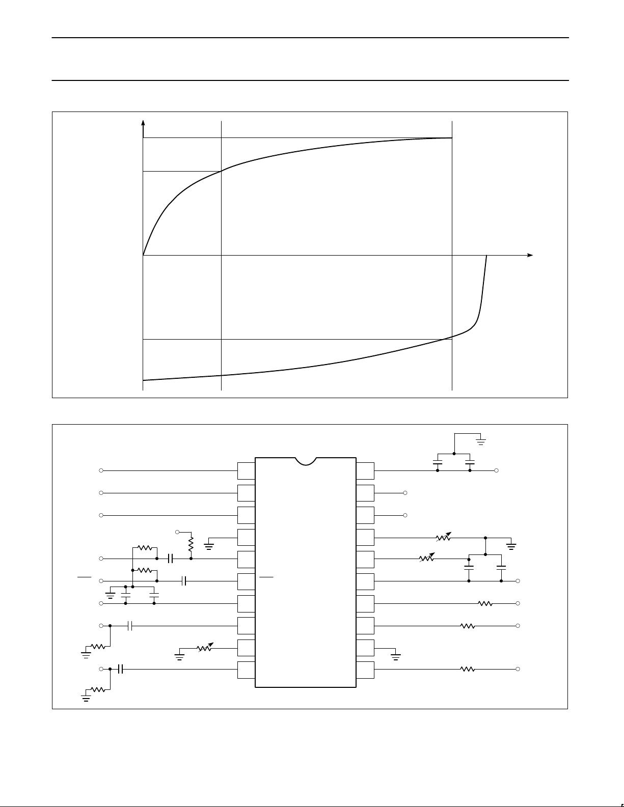
2. The relative output current variation is defined thus:
I
OUT
I
OUT
2
(I
2
I1)
|(I
2
I1)|
; with V1 = 0.7V, V2 = V
DDA
– 0.8V (see Figure 3).
3. F
RD
is the value of the 3 bit fractional accumulator.
4. Monotonicity is guaranteed with C
N
= 0 to 255.
5. Power supply current measured with f
RF_IN
= 1667.4MHz, NM1 = 0, NM2 = 1, NM3 = 1, NM4 = 4, FMOD = 8, N = 694 6/8, main phase
detector frequency = 2.4MHz, f
REF IN
= 19.2MHz, NR = 8, SM = 1, f
AUX_IN
= 150MHz, NA = 125, SA = 1, PA = 0, auxiliary phase detector
frequency = 300kHz, IRN = IRA = IRF = 25µA, CN = 160, CL = 0, CK = 0, lock condition, normal mode, V
CCP
= VDD = V
DDA
= 3V.
Operational supply current = I
DDA
+ IDD + I
CCP
.
6. Specification condition: CN = 255
7. Specification conditions:
1) CN = 255; CL = 1, or
2) CN = 75; CL = 3
8. Typical output current | I
PHI
| = –IRN x CN x 2
(CL+1)
x CK/32:
1) CN = 160; CL = 3; CK = 1, or
2) CN = 160; CL = 2; CK = 2, or
3) CN = 160; CL = 1; CK = 4, or
4) CN = 160; CL = 0; CK = 8
9. Any RFD, CL = 1 for speed-up pump. The integral pump is intended for switching only and the fractional compensation is not guaranteed.
10.Specification conditions: F
RD
= 1 to 7; CL = 1.
11.Specification conditions:
1) F
RD
= 1 to 7; CL = 1; CK = 2, or
2) F
RD
= 1 to 7; CL = 2; CK = 1.
12.The matching is defined by the sum of the P and the N pump for a given output voltage.
13.Limited analog supply voltage range 4.5 to 5.5V.
14.For f
IN
< 50MHz, low frequency operation requires DC-coupling and a minimum input slew rate of 32V/µs.
15.Guaranteed by design.
16.F
XTAL
= 14.4MHz, V
XTAL
= 500mV
P-P
, comparison Freq. = 200kHz, Loop bandwidth = 5kHz, Audio filter = 300Hz to 15kHz.
t
Pulse width; STROBE
SW
1
f
VCO
1
f
VCO
1
f
VCO
ns
Page 8
Philips Semiconductors Product specification
SA8025A1.8GHz low-voltage Fractional-N synthesizer
1996 Oct 15
8
I
2
I
1
I
2
I
1
V
1
V
2
CURRENT
VOLTAGE
SR00625
Figure 3. Relative Output Current Variation
1
2
3
4
5
6
7
8
9
10
11
12
13
14
20
19
18
17
16
15
CLOCK
DATA
STROBE
V
SS
RF
IN
RF
IN
V
CCP
REF
IN
RA
AUX
IN
V
DD
TEST
LOCK
RF
RN
V
DDA
PHP
PHI
V
SSA
PHA
SA8025A
V
DD
A
V
PH
P
V
PHI
V
PH
A
V
DD
CLOCK
DATA
STROBE
RF
IN
RF
IN
V
CCP
REF
IN
AUX
IN
150k
TEST
22nF
RF
150k
22nF
1k
RN
100
1k
22nF
50
50
22nF
22nF
150k
22nF
22nF
50
50
10µF
10µF
10µF
LOCK
10K
SR00626
Figure 4. Test Circuit
Page 9
Philips Semiconductors Product specification
SA8025A1.8GHz low-voltage Fractional-N synthesizer
1996 Oct 15
9
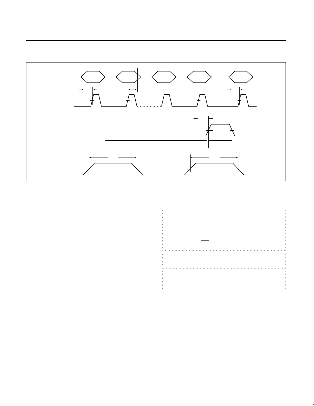
AC TIMING CHARACTERISTICS
DATA
D0 D1
t
SW
CLOCK
STROBE
CLOCK ENABLED CLOCK
DISABLED
STORE DATA
SHIFT IN DATA
CLOCK
STROBE (B, C, D, E) WORDS
STROBE
(A WORD)
t
W
50% 50%
t
SU
LAST CLOCK FIRST CLOCKFIRST CLOCK
50%
t
SU
t
H
t
SU
D0
D22,
D30
D23,
D31
SR00627
Figure 5. Serial Input Timing Sequence
FUNCTIONAL DESCRIPTION
Serial Input Programming
The serial input is a 3-wire input (CLOCK, STROBE, DATA) to
program all counter ratios, DACs, selection and enable bits. The
programming data is structured into 24 or 32 bit words; each word
includes 1 or 4 address bits. Figure 5 shows the timing diagram of
the serial input. When the STROBE = L, the clock driver is enabled
and on the positive edges of the CLOCK the signal on DATA input is
clocked into a shift register. When the STROBE = H, the clock is
disabled and the data in the shift register remains stable.
Depending on the 1 or 4 address bits the data is latched into
different working registers or temporary registers. In order to fully
program the synthesizer, 4 words must be sent: D, C, B and A.
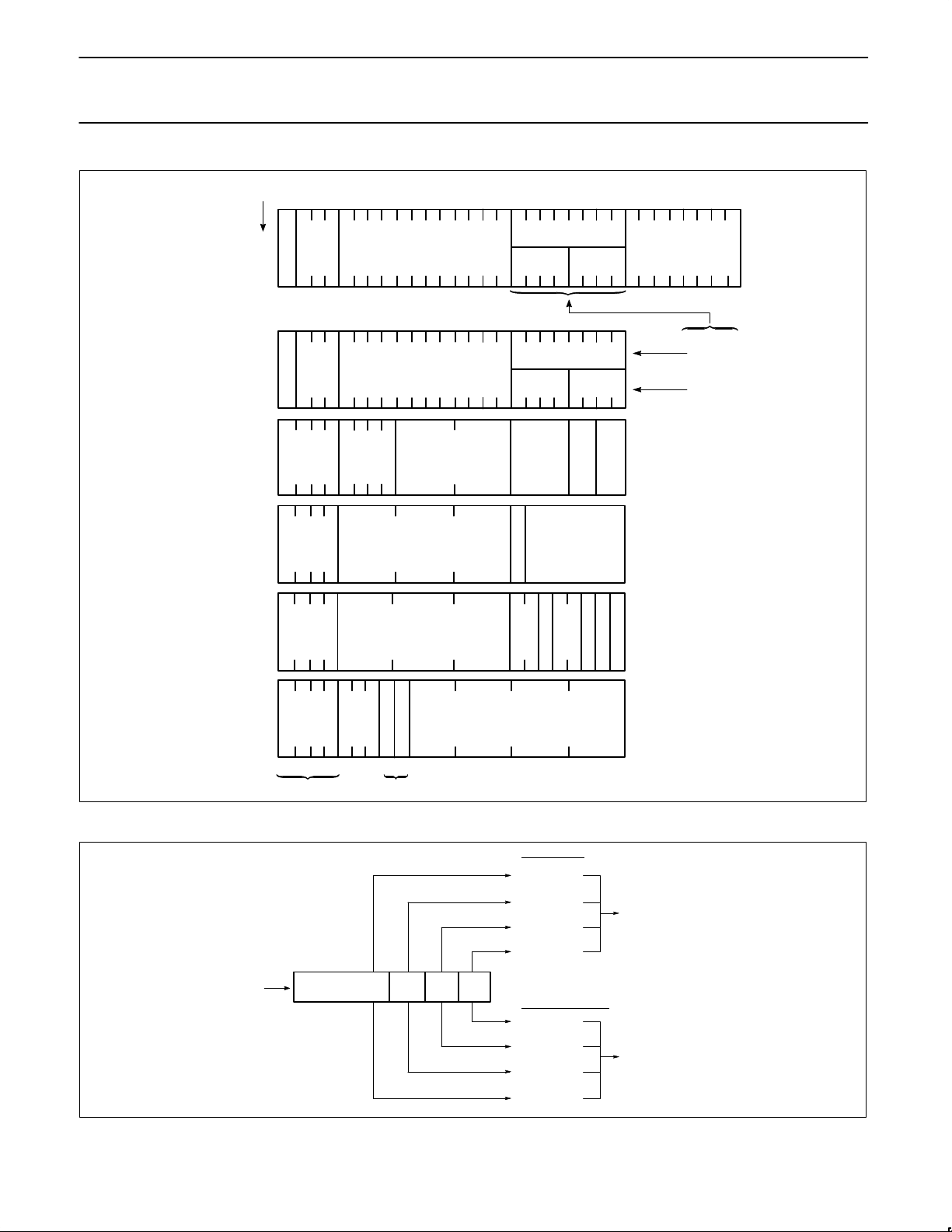
Figure 6 and Table 1 shows the format and the contents of each
word. The E word is for testing purposes only. The E (test) word is
reset when programming the D word. The data for CN and PR is
stored by the B word in temporary registers. When the A word is
loaded, the data of these temporary registers is loaded together with
the A word into the work registers which avoids false temporary
main divider input. CN is only loaded from the temporary registers
when a short 24 bit A0 word is used. CN will be directly loaded by
programming a long 32 bit A1 word. The flag LONG in the D word
determines whether A0 (LONG = “0”) or A1 (LONG = “1”) format is
applicable. The A word contains new data for the main divider.
Main Divider Synchronization
The A word is loaded only when a main divider synchronization
signal is also active in order to avoid phase jumps when
reprogramming the main divider. The synchronization signal is
generated by the main divider. The signal is active while the NM1
divider is counting down from the programmed value. The new A
word will be loaded after the NM1 divider has reached its terminal
count; also, at this time a main divider output pulse will be sent to
the main phase detector. The loading of the A word is disabled
while the other dividers are counting up to their programmed values.
Therefore, the new A word will be correctly loaded provided that the
STROBE signal has been at an active high value for at least a
minimum number of VCO input cycles at RF
IN
or RFIN.
(NM2 65) t
W
For PR = ‘01’
[NM2 65 (NM3 1) 68] t
W
For PR = ‘10’
[(NM2 65 (NM3 1)
68 (NM4 1) 73)] t
W
For PR = ‘11’
[(NM2 65) (NM4 1) 73] t
W
For PR = ‘00’
f
1
VCO
f
VCO
1
t_strobe_min
t_strobe_min
t_strobe_min
t_strobe_min
f
f
1
VCO
1
VCO
Programming the A word means also that the main charge pumps
on output PHP and PHI are set into the speed-up mode as long as
the STROBE is H.
Auxiliary Divider
The input signal on AUX_IN is amplified to logic level by a
single-ended CMOS input buffer, which accepts low level AC
coupled input signals. This input stage is enabled if the serial
control bit EA = “1”. Disabling means that all currents in the input
stage are switched off. A fixed divide by 4 is enabled if PA = “0”.
This divider has been optimized to accept a high frequency input
signal. If PA = “1”, this divider is disabled and the input signal is fed
directly to the second stage, which is a 12-bit programmable divider
with standard input frequency (40MHz). The division ratio can be
expressed as:
if PA = “0”: N = 4 x NA
Page 10

Philips Semiconductors Product specification
SA8025A1.8GHz low-voltage Fractional-N synthesizer
1996 Oct 15
10
if PA = “1”: N = NA; with NA = 4 to 4095
Reference Divider
The input signal on REF_IN is amplified to logic level by a
single-ended CMOS input buffer, which accepts low level AC
coupled input signals. This input stage is enabled by the OR
function of the serial input bits EA and EM. Disabling means that all
currents in the input stage are switched off. The reference divider
consists of a programmable divider by NR (NR = 4 to 4095) followed
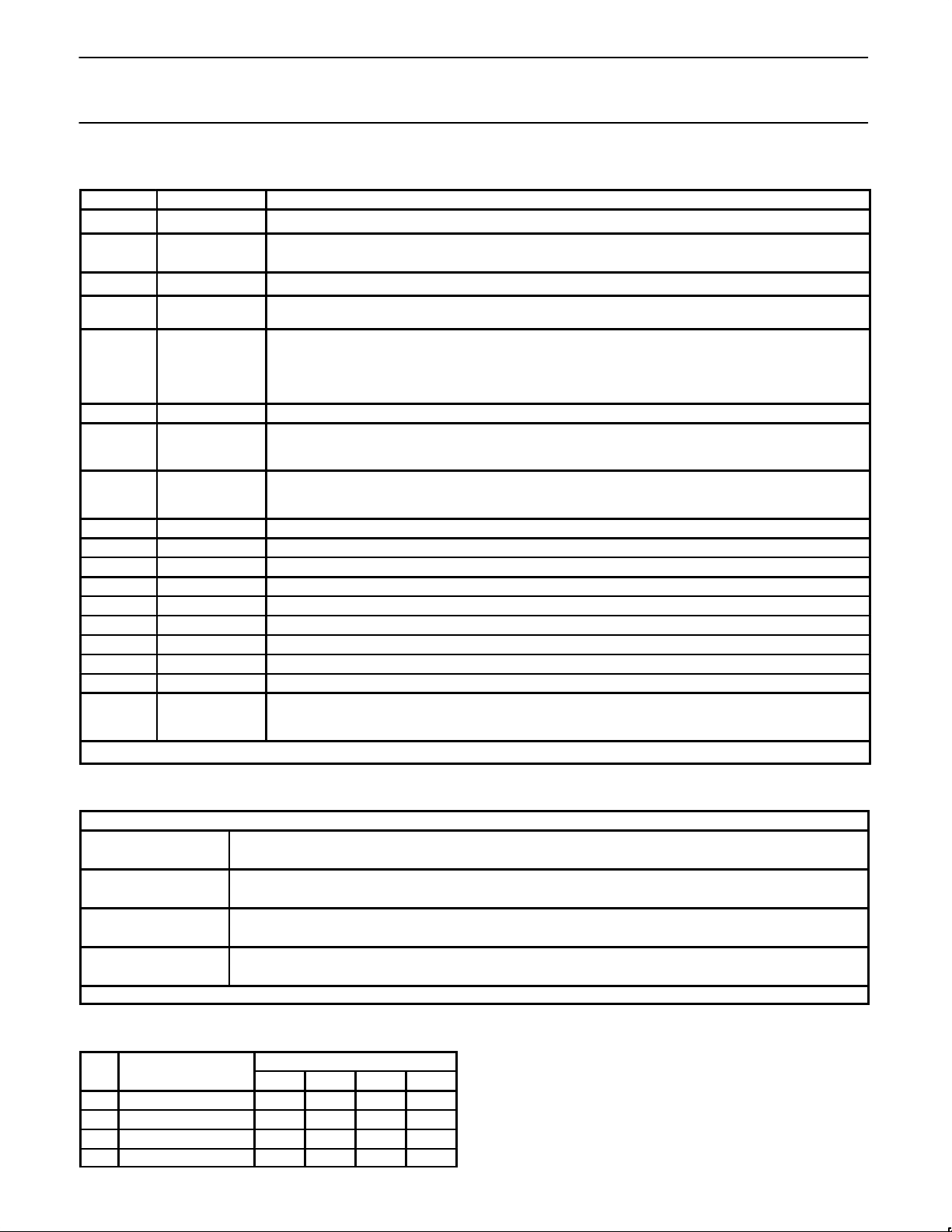
by a three bit binary counter. The 2 bit SM register (see Figure 7)
determines which of the 4 output pulses is selected as the main
phase detector input. The 2 bit SA register determines the selection
of the auxiliary phase detector signal.
Main Divider
The differential inputs are amplified (to internal ECL logic levels) and
provide excellent sensitivity (–20dBm at 1.7GHz) making the
prescaler ideally suited to directly interface to a VCO as integrated
on the Philips front-end devices including RF gain stage, VCO and
mixer. The internal four modulus prescaler feedback loop FB
controls the selection of the divide by ratios 64/65/68/73, and
reduces the minimum system division ratio below the typical value
required by standard dual modulus (64/65) devices.
This input stage is enabled when serial control bit EM = “1”.
Disabling means that all currents in the prescaler are switched off.
The main divider is built up by a 12 bit counter plus a sign bit.
Depending on the serial input values NM1, NM2, NM3, NM4 and the
prescaler select PR, the counter will select a prescaler ratio during a
number of input cycles according to Table 2 and Table 3.
The loading of the work registers NM1, NM2, NM3, NM4 and PR is
synchronized with the state of the main counter, to avoid extra
phase disturbance when switching over to another main divider ratio
as explained in the Serial Input Programming section.
At the completion of a main divider cycle, a main divider output
pulse is generated which will drive the main phase comparator.
Also, the fractional accumulator is incremented with NF. The
accumulator works modulo Q. Q is preset by the serial control bit
FMOD to 8 when FMOD = “1”. Each time the accumulator
overflows, the feedback to the prescaler will select one cycle using
prescaler ratio R2 instead of R1.
As shown above, this will increase the overall division ratio by 1 if
R2 = R1 + 1. The mean division ratio over Q main divider will then
be
NQ N
NF
Q
Programming a fraction means the prescaler with main divider will
divide by N or N + 1. The output of the main divider will be
modulated with a fractional phase ripple. This phase ripple is
proportional to the contents of the fractional accumulator FRD,
which is used for fractional current compensation.
Page 11
Philips Semiconductors Product specification
SA8025A1.8GHz low-voltage Fractional-N synthesizer
1996 Oct 15
11
MSB
LSB
WORD
A1
A0
B
C
D
E
ADDRESS BITS TEST BITS
D31 D0
0 NF NM1
NM2
NM3 NM2
CN
D0
0 NF NM1
NM2
NM3 NM2
D23
PR = “01”
PR ≠ “01”
1 0 0 0 CN CK CL PR
1 0 0 NA1
P
A
1 0 1 NR0 SM
E
M
SA
E
A
F
M
O
D
L
O
N
G
1 1 1 1
D23 D0
NM4
0 0 0
T1T
0
0
0
LAST IN FIRST IN
SR00628
Figure 6. Serial Input Word Format
SA = “11”
SA = “10”
SA = “01”
SA = “00”
SM = “11”
SM = “10”
SM = “01”
SM = “00”
MAIN SELECT
AUXILIARY SELECT
REFERENCE
INPUT
DIVIDE BY NR ÷2
MAIN
DETECTOR
PHASE
AUXILIARY
DETECTOR
PHASE
÷2 ÷2
SR00629
Figure 7. Reference Divider
Page 12
Philips Semiconductors Product specification
SA8025A1.8GHz low-voltage Fractional-N synthesizer
1996 Oct 15
12
Table 1. Function Table
Symbol Bits Function
NM1 12
Number of main divider cycles when prescaler modulus = 64*
NM2
8 if PR = “01”
4 if PR = “10”
Number of main divider cycles when prescaler modulus = 65*
NM3 4 if PR = “10”
Number of main divider cycles when prescaler modulus = 68*
NM4
4 if PR = “11” or
“00”
Number of main divider cycles when prescaler modulus = 73*
PR 2 Prescaler type in use
PR = “01”: modulus 2 prescaler (64/65)
PR = “10”: modulus 3 prescaler (64/65/68)
PR = “11”: modulus 4 prescaler (64/65/68/73)
PR = “00”: modulus 3 prescaler (64/65/73)
NF 3 Fractional-N increment
FMOD 1 Fractional-N modulus selection flag
“1”: modulo 8
“0”: modulo 5
LONG 1 A word format selection flag
“0”: 24 bit A0 format
“1”: 32 bit A1 format
CN 8 Binary current setting factor for main charge pumps
CL 2 Binary acceleration factor for proportional charge pump current
CK 4 Binary acceleration factor for integral charge pump current
EM 1 Main divider enable flag
EA 1 Auxiliary divider enable flag
SM 2 Reference select for main phase detector
SA 2 Reference select for auxiliary phase detector
NR 12 Reference divider ratio
NA 12 Auxiliary divider ratio
PA 1
Auxiliary prescaler mode:
PA = “0”: divide by 4
PA = “1”: divide by 1
*Not including reset cycles and Fractional-N effects.
Table 2. Prescaler Ratio
The total division ratio from prescaler to the phase detector may be expressed as:
if PR = “01” N = (NM1 + 2) x 64 + NM2 x 65
N’ = (NM1 + 1) x 64 + (NM2 + 1) x 65 (*)
if PR = “10” N = (NM1 + 2) x 64 + NM2 x 65 + (NM3 + 1) x 68
N’ = (NM1 + 1) x 64 + (NM2 + 1) x 65 + (NM3 + 1) x 68 (*)
if PR = “11” N = (NM1 + 2) x 64 + NM2 x 65 + (NM3 + 1) x 68 + (NM4 + 1) x 73
N’ = (NM1 + 1) x 64 + (NM2 + 1) x 65 + (NM3 + 1) x 68 + (NM4 + 1) x 73 (*)
if PR = “00” N = (NM1 + 2) x 64 + NM2 x 65 + (NM4 + 1) x 73
N’ = (NM1 + 1) x 64 + (NM2 + 1) x 65 + (NM4 + 1) x 73 (*)
(*) When the fractional accumulator overflows the prescaler ratio = 65 (64 + 1) and the total division ratio N’ = N + 1
Table 3. PR Modulus
Bit Capacity
PR
Modulus Prescaler
NM1 NM2 NM3 NM4
01 2 12 8 – –
10 3 12 4 4 –
11 4 12 4 4 4
00 3 12 8 – 4
Page 13
Philips Semiconductors Product specification
SA8025A1.8GHz low-voltage Fractional-N synthesizer
1996 Oct 15
13
REF_IN
REFERENCE
DIVIDER
AUX/MAIN
DIVIDER
L
“1”
R
DCQ
R
D
C
Q
R
“1”
X
P
N
N-TYPE
CHARGE PUMP
PH
P-TYPE
CHARGE PUMP
V
DDA
V
SSA
REF_IN
L
R
X
P
N
I
PH
SR00630
Figure 8. Phase Detector Structure with Timing
Phase Detectors
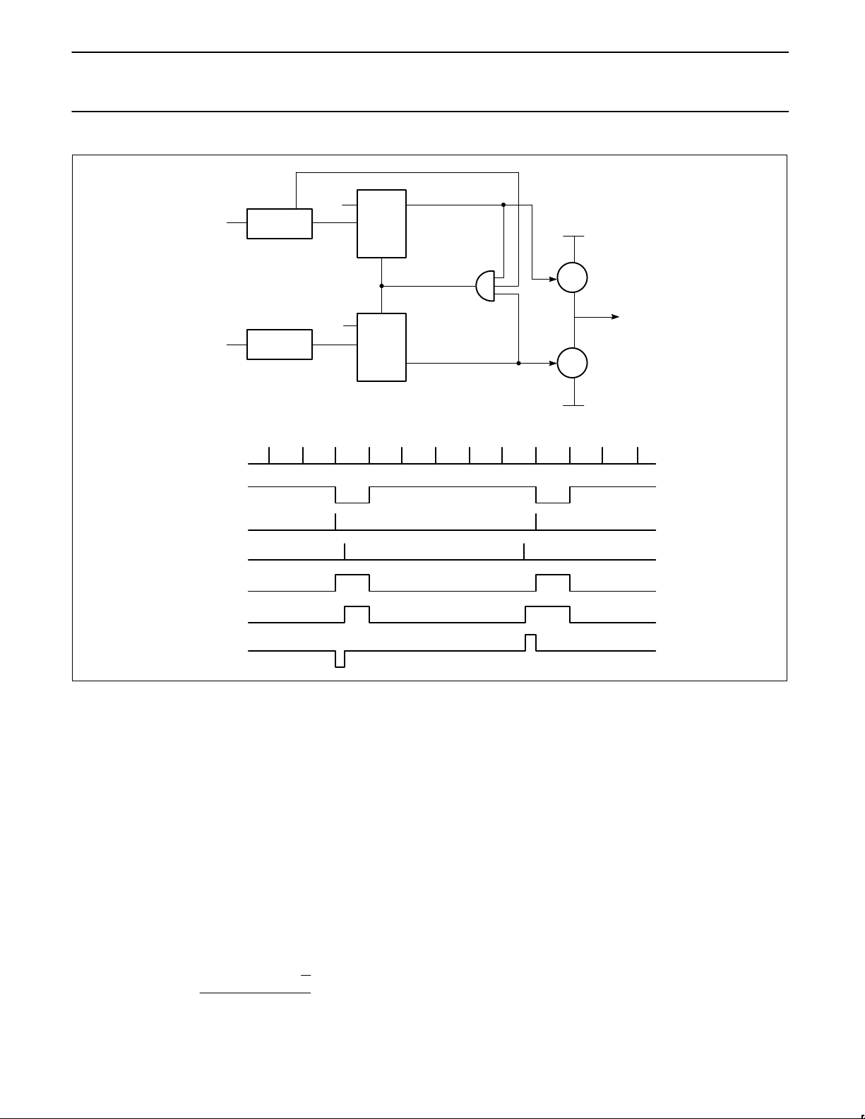
The auxiliary and main phase detectors are a two D-type flip-flop
phase and frequency detector shown in Figure 8. The flip-flops are
set by the negative edges of output signals of the dividers. The
rising edge of the signal, L, will reset the flip-flops after both flip-flops
have been set. Around zero phase error this has the effect of
delaying the reset for 1 reference input cycle. This avoids
non-linearity or deadband around zero phase error. The flip-flops
drive on-chip charge pumps. A source current from the charge
pump indicates the VCO frequency will be increased; a sink current
indicates the VCO frequency will be decreased.
Current Settings
The SA8025A has 3 current setting pins: RA, RN and RF. The
active charge pump currents and the fractional compensation
currents are linearly dependent on the current connected between
the current setting pin and V
SS
. The typical value R (current setting
resistor) can be calculated with the formula:
R +
V
DDA
* 0.9 * 150 I
R
Ǹ
I
R
The current can be set to zero by connecting the corresponding pin
to V
DDA
.
Auxiliary Output Charge Pumps
The auxiliary charge pumps on pin PHA are driven by the auxiliary
phase detector and the current value is determined by the external
resistor RA at pin RA. The active charge pump current is typically:
|I
PHA
| + 8 @ I
RA
Page 14
Philips Semiconductors Product specification
SA8025A1.8GHz low-voltage Fractional-N synthesizer
1996 Oct 15
14
REFERENCE R
MAIN N
DETECTOR
OUTPUT
CONTENTS
ACCUM.
FRACTIONAL
COMPENSATION
CURRENT
N N N + 1 N N + 1
2 4 1 3 0
PULSE-WIDTH
MODULATION
OUTPUT ON
PHP, PHI
PULSE-LEVEL
MODULATION
mA
µA
TIME
VCO CYCLES
SR00560
Figure 9. Waveforms for NF = 2, Fraction = 0.4
Main Output Charge Pumps and Fractional
Compensation Currents
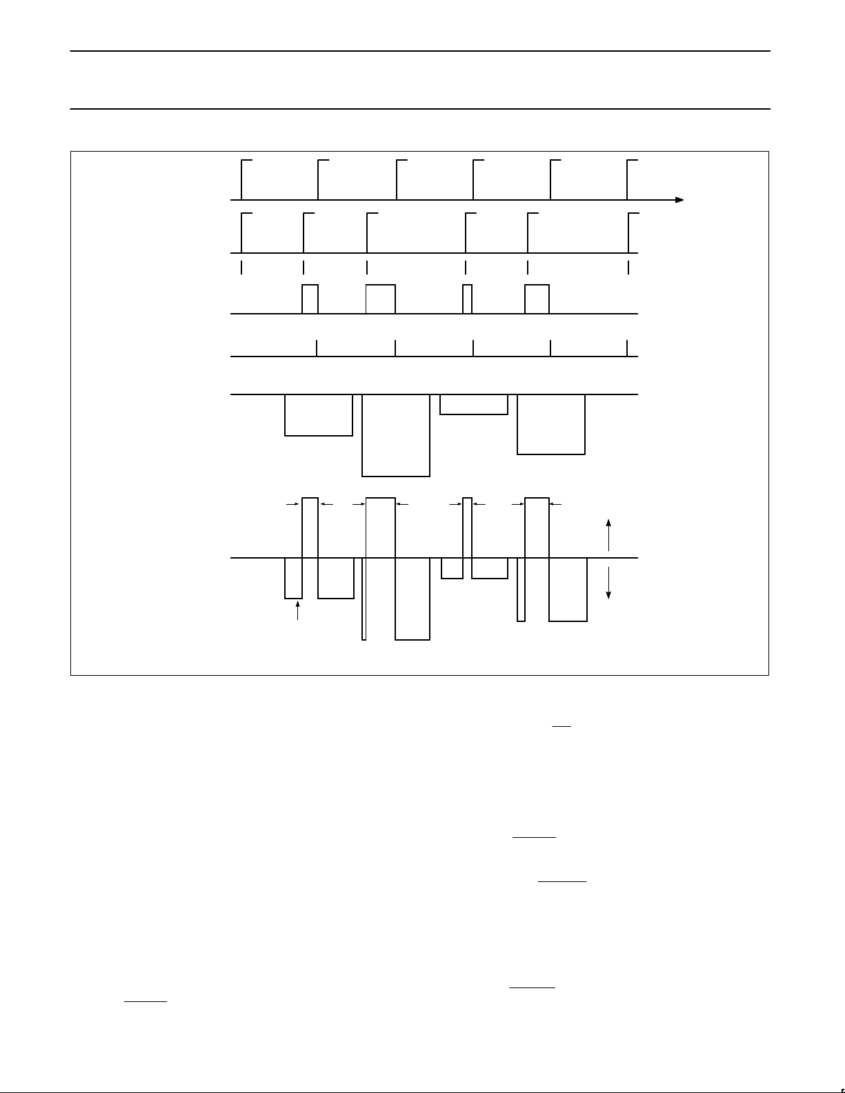
The main charge pumps on pin PHP and PHI are driven by the main
phase detector and the current value is determined by the current at
pin RN and via a number of DACs which are driven by registers of
the serial input. The fractional compensation current is determined
by the current at pin RF, the contents of the fractional accumulator
FRD and a number of DACs driven by registers from the serial input.
The timing for the fractional compensation is derived from the
reference divider. The current is on during 1 input reference cycle
before and 1 cycle after the output signal to the phase comparator.
Figure 9 shows the waveforms for a typical case.
When the serial input A word is loaded, the output circuits are in the
“speed-up mode” as long as the STROBE is H, else the “normal
mode” is active. In the “normal mode” the current output PHP is:
I
PHP_N
+ I
PHP
) I
PHP_comp
where:
|I
PHP
| +
CN @ I
RN
32
:charge pump current
|I
PHP_comp
| + FRD @
I
RF
128
:fractional comp.
current
The current in PHI is zero in “normal mode”.
In “speed-up mode” the current in output PHP is:
I
PHP_S
+ I
PHP
) I
PHP_comp
|I
PHP
| +
ǒ
CN @ I
RN
32
Ǔ
(2
CL)1
) 1)
|I
PHP_comp
| +
ǒ
FRD @ I
RF
128
Ǔ
(2
CL)1
) 1)
In “speed-up mode” the current in output PHI is:
I
PHI_S
+ I
PHI
) I
PHI_comp
where:
|I
PHI
| +
ǒ
CN @ I
RN
32
Ǔ
(2
CL)1
) CK
Page 15
Philips Semiconductors Product specification
SA8025A1.8GHz low-voltage Fractional-N synthesizer
1996 Oct 15
15
|I
PHI_comp
| +
ǒ
FRD @ I
RN
128
Ǔ
(2
CL)1
) CK
Figure 9 shows that for proper fractional compensation, the area of
the fractional compensation current pulse must be equal to the area
of the charge pump ripple output. This means that the current
setting on the input RN, RF is approximately:
[
(Q @ f
VCO
)
(3 @ CN@ F
)
MAIN
DIVIDER
REF
DIVIDER
AUX
DIVIDER
SM
LOCK
T1
T0
φ
MAIN
φ
AUX
SELECT
LOGIC
SR00561
Figure 10. Test Mode Diagram
I
RN
I
where:
Q = fractional-N modulus
f
= f
VCO
F
INR
× N, input frequency of the prescaler
INM
= input frequency of the reference divider
PHI pump is meant for switching only. Current and compensation
are not as accurate as PHP.
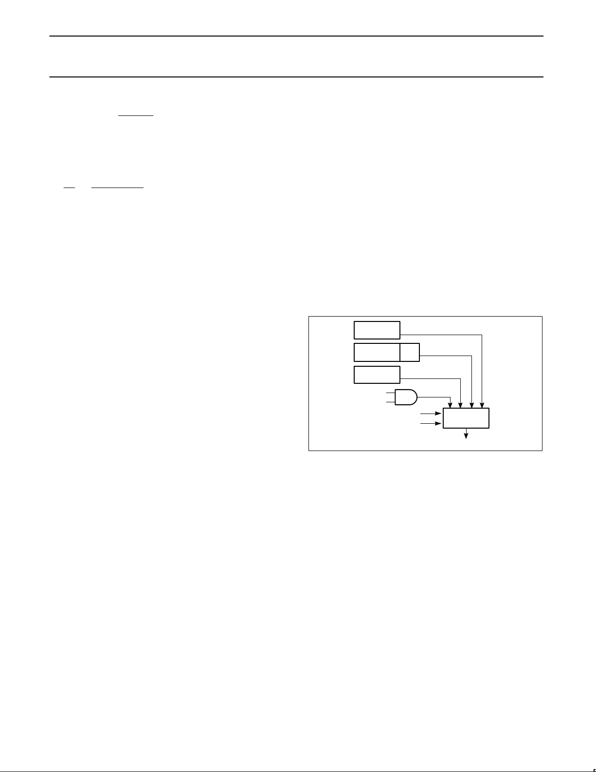
Lock Detect
The output LOCK is H when the auxiliary phase detector AND the
main phase detector indicates a lock condition. The lock condition
is defined as a phase difference of less than +1 cycle on the
reference input REF_IN. The lock condition is also fulfilled when the
relative counter is disabled (EM = “0” or respectively EA = “0”) for
the main, respectively auxiliary counter.
Test Modes
The lock output is selectable as f
and T0 of the E word control the selection (see Figures 6 and 10).
If T1 = T0 = Low, or if the E-word is not sent, the lock output is
configured as the normal lock output described in the Lock Detect
section.
If T1 = Low and T0 = High, the lock output is configured as f
The signal is the buffered output of the reference divider NR and the
3-bit binary counter SM. The f
and pulses high whenever the divider reaches terminal count from
the value programmed into the NR and SM registers. The f
signal can be used to verify the divide ratio of the Reference divider.
, f
, f
REF
AUX
signal appears as normally low
REF
and lock. Bits T1
MAIN
REF
REF
.
If T1 = High and T0 = Low, the lock output is configured as f
AUX
.
The signal is normally high and pulses low whenever the divider
reaches terminal count from the value programmed into the NA and
PA registers. The f
signal can be used to verify the divide ratio
AUX
of the Auxiliary divider.
If T1 = High and T0 = High, the lock output is configured as f
The signal is the buffered output of the MAIN divider. The f
MAIN
MAIN
.
signal appears as normally high and pulses low whenever the
divider reaches terminal count from the value programmed into the
NM1, NM2, NM3 or NM4 registers. The f
signal can be used to
MAIN
verify the divide ratio of the MAIN divider and the prescaler.
Test Pin
The Test pin, Pin 19, is a buffered logic input which is exclusively
ORed with the output of the prescaler. The output of the XOR gate
is the input to the MAIN divider. The Test pin must be connected to
V
during normal operation as a synthesizer. This pin can be used
DD
as an input for verifying the divide ratio of the MAIN divider; while in
this condition the input to the prescaler, RF
V
through a 10kΩ resistor in order to place prescaler output into
CCP
a known state.
, may be connected to
IN
Page 16
Philips Semiconductors Product specification
SA8025A1.8GHz low-voltage Fractional-N synthesizer
1996 Oct 15
16
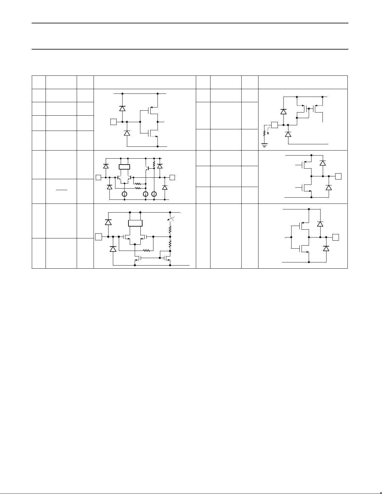
PIN FUNCTIONS
5
PIN
No.
PIN
MNEMONIC
DC V EQUIVALENT CIRCUIT
PIN
No.
PIN
MNEMONIC
DC V EQUIVALENT CIRCUIT
1 CLOCK ––
2 DATA ––
18 LOCK ––
3 STROBE ––
19 TEST ––
5 RF
IN
2.1
V
DD
V
SS
6
6 RF
IN
2.1
2.5k
2.5k
V
CCP
= 3V
V
SS
10
100k
8 REF
IN
1.8
10 AUX
IN
1.8
V
DDA
= 3V
V
SS
ENABLE
9 RA 1.35
16 RN 1.35
17 RF 1.35
V
DDA
= 3V
V
SSA
25µA
9
11 PHA ––
13 PHI ––
14 PHP ––
V
DDA
V
SSA
11
18
V
DD
V
SS
1
SR00562
Figure 11. Pin Functions
Page 17
Philips Semiconductors Product specification
SA8025A1.8GHz low-voltage Fractional-N synthesizer
1996 Oct 15
17
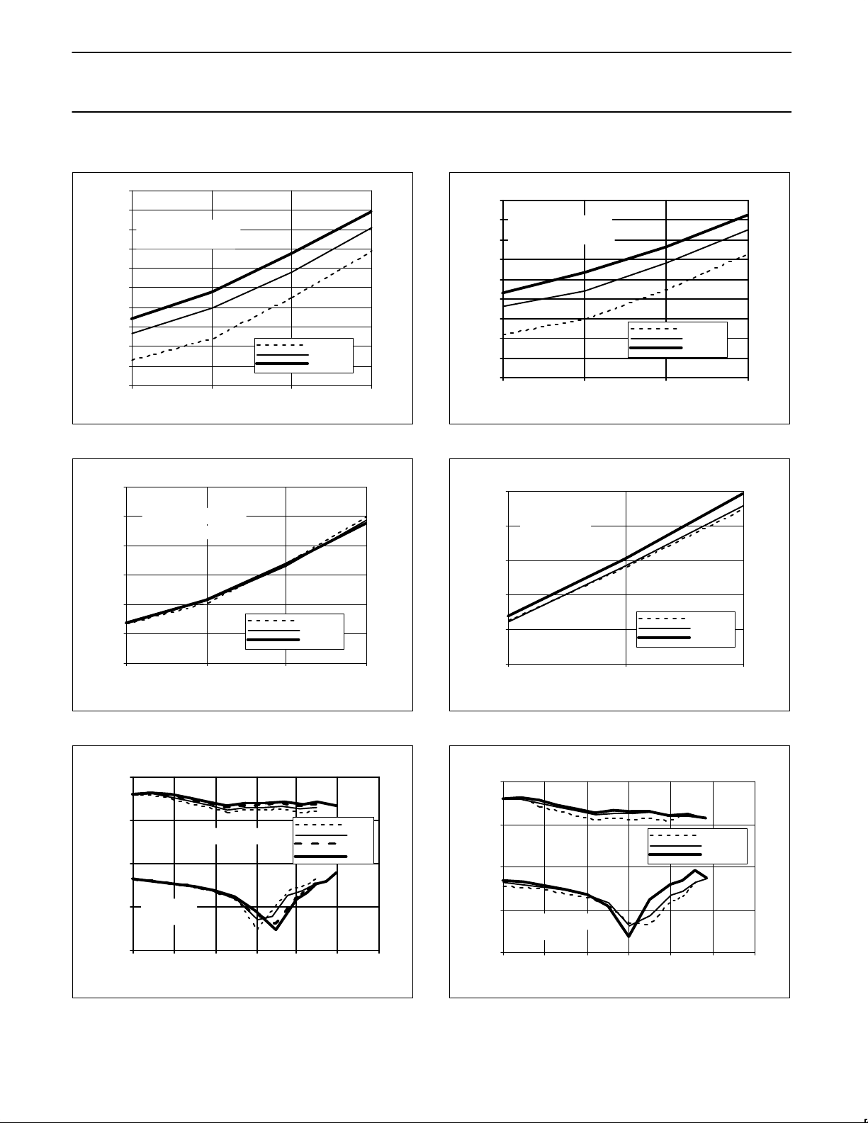
TYPICAL PERFORMANCE CHARACTERISTICS
SUPPLY VOLTAGE (V)
V
CCP
= V
DDA
= V
DD
EA=0, EM=1, Note5
18
2.7 3.5 4.5 5.5
I TOTAL (mA)
t = –40°C
t = 25°C
t = 85°C
17
16
15
14
13
12
11
10
9
8
SR00563
Figure 12. Operational Supply Current vs Supply Voltage and
Temperature
SUPPLY VOLTAGE (V)
V
CCP
= V
DDA
= V
DD
EA=1, EM=0, Note5
7
2.7 3.5 4.5 5.5
I TOTAL (mA)
6
5
4
3
2
1
t = –40°C
t = 25°C
t = 85°C
SR00564
Figure 13. Auxiliary Operational Supply Current vs Supply
Voltage and Temperature
TA = 25°C,
N = 196
2.7V
3.5V
4.5V
5.5V
VDD = V
CCP
FREQUENCY (MHz)
20
1100
INPUT POWER (dBm)
0
–20
–40
–60
1300
1500
1700
1900
2100
2300
SR00565
Figure 14. Main Divider Input Power vs Frequency and Supply
t = –40°C
t = 25°C
t = 85°C
SUPPLY VOLTAGE (V)
15
2.7 3.5 4.5 5.5
I TOTAL (mA)
14
13
12
11
10
9
8
7
6
V
CCP
= V
DDA
= V
DD
EM = 0, EA = 1, Note5
SR00566
Figure 15. Main Operational Supply Current vs Supply Voltage
and Temperature
AUXILIARY INPUT FREQUENCY (MHz)
VDD = 3V, V
DDA
= 5V
Pin = –10dBm,
ref divider halted
3.5
50 100 150
I TOTAL (mA)
3
2.5
2
1.5
1
t = –40°C
t = 25°C
t = 85°C
SR00567
Figure 16. Auxiliary Operational Supply Current vs Frequency
and Temperature
t=–40°C
t=25°C
t=85°C
FREQUENCY (MHz)
20
INPUT POWER (dBm)
0
–20
–40
–60
VDD = V
CCP
= 3V
N = 196
1100
1300
1500
1700
1900
2100
2300
SR00568
Figure 17. Main Divider Input Power vs Frequency and
Temperature
Page 18
Philips Semiconductors Product specification
SA8025A1.8GHz low-voltage Fractional-N synthesizer
1996 Oct 15
18
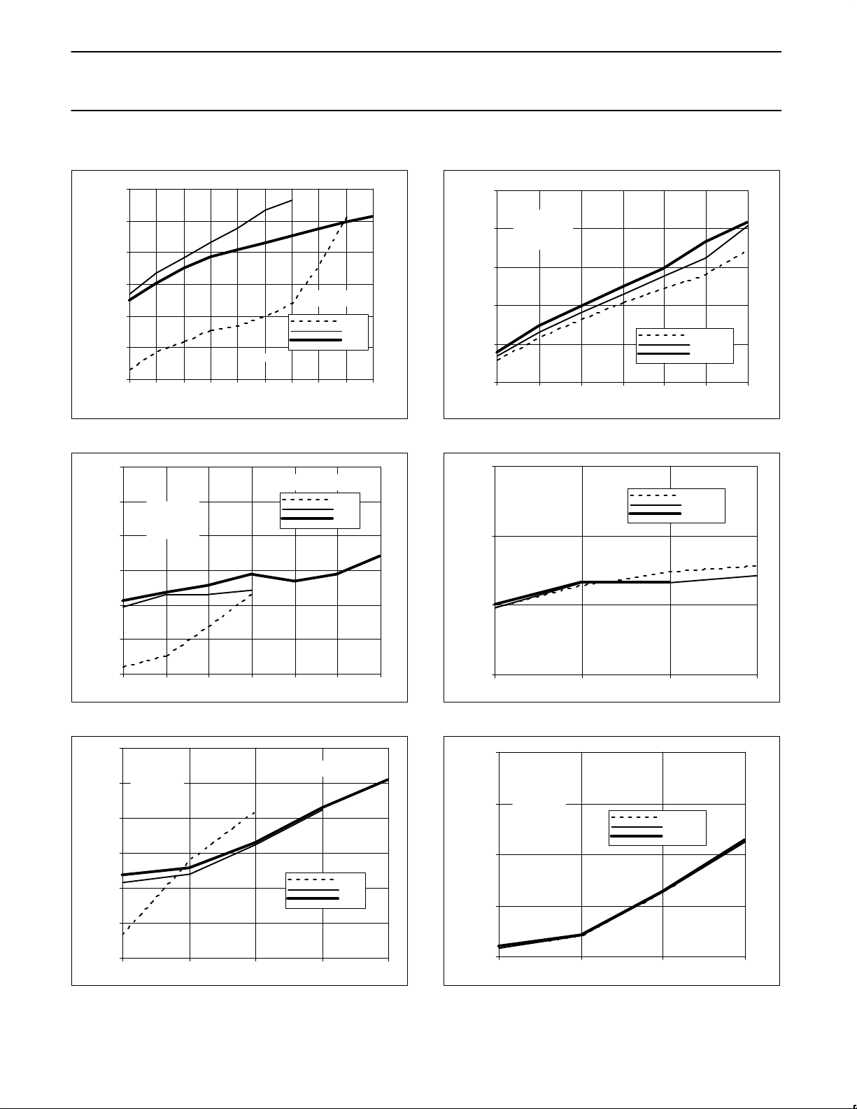
TYPICAL PERFORMANCE CHARACTERISTICS (Continued)
3/3V
3/5V
5/5V
N=100
VDD/V
DDA
10 15 20 25 30 35 40 45 50 55
0
–5
–10
–15
–20
–25
–30
INPUT POWER (dBm)
FREQUENCY (MHz)
SR00569
Figure 18. Reference Divider Minimum Input Power vs
Frequency and Supply
MINIMUM INPUT POWER (dBm)
T
A
=amb,
PA=1,
N=100
30 50 70 90 110 130 150
FREQUENCY (MHz)
0
–5
–10
–15
–20
–25
–30
VDD/V
DDA
3/3V
3/5V
5/5V
SR00570
Figure 19. Auxiliary Divider Minimum Input Power vs
Frequency and Supply
T
A
= amb,
PA=0,
N=25
50 100 150 200 250
FREQUENCY (MHz)
0
VDD/V
DDA
–5
–10
–15
–20
–25
–30
MINIMUM INPUT POWER (dBm)
3/3V
3/5V
5/5V
SR00571
Figure 20. Auxiliary Divider Minimum Input Power vs
Frequency and Supply
10 15 20 25 30 35 40
5
MINIMUM INPUT POWE (dBm)
FREQUENCY (dBm)
0
–5
–10
–15
–20
VDD= 3V,
V
DDA
= 5V,
N = 100
t = –40°C
t = 25°C
t = 85°C
SR00572
VDD =3V,
V
DDA
=5V,
PA=1,
N=100
30 50 70 90
FREQUENCY (MHz)
–10
–15
–20
–25
MINIMUM INPUT POWER (dBm)
t = –40°C
t = 25°C
t = 85°C
SR00573
Figure 22. Auxiliary Divider Minimum Input Power vs
Frequency and Temperature
VDD=3V,
V
DDA
=5V
50 100 150 200
FREQUENCY (MHz)
0
–5
–10
–15
–20
MINIMUM INPUT POWER (dBm)
t = –40°C
t = 25°C
t = 85°C
PA=0,
N=25
SR00574
Figure 23. Auxiliary Divider Minumum Input Power vs
Frequency and Temperature
Figure 21. Reference Divider Minimum Input Power vs
Frequency and Temperature
Page 19
Philips Semiconductors Product specification
SA8025A1.8GHz low-voltage Fractional-N synthesizer
1996 Oct 15
19
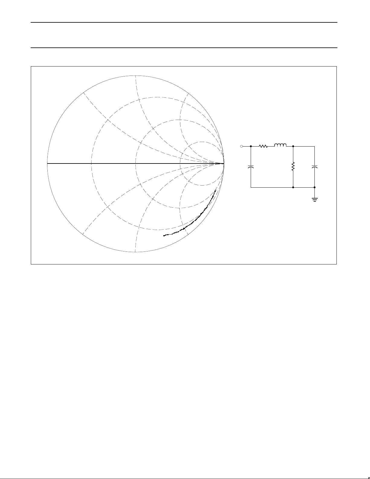
–j1
–j2
j2
j1
j0.5
0
–j0.5
R3 L4
C2
R1
C1
0.1pF
0.8pF
2500Ω
4Ω
2nH
Equivalent Input Impedance
1
V
CCP
= VDD = 3V
T
A
= 25°C
2000
1600
1200
800
500
SR00575
Figure 24. Typical RFIN Input Impedance
Page 20
Philips Semiconductors Product specification
SA8025A1.8GHz low-voltage Fractional-N synthesizer
1996 Oct 15
20
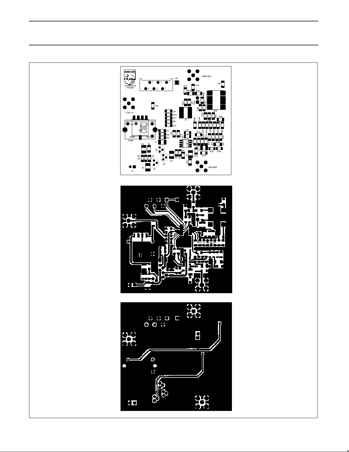
TOP SILK SCREEN
TOP VIEW
BOTTOM VIEW
SR00576
Figure 25. SA8025ADK Demoboard Layout (NOT ACTUAL SIZE)
Page 21
Philips Semiconductors Product specification
SA8025A1.8GHz low-voltage Fractional-N synthesizer
1996 Oct 15
21
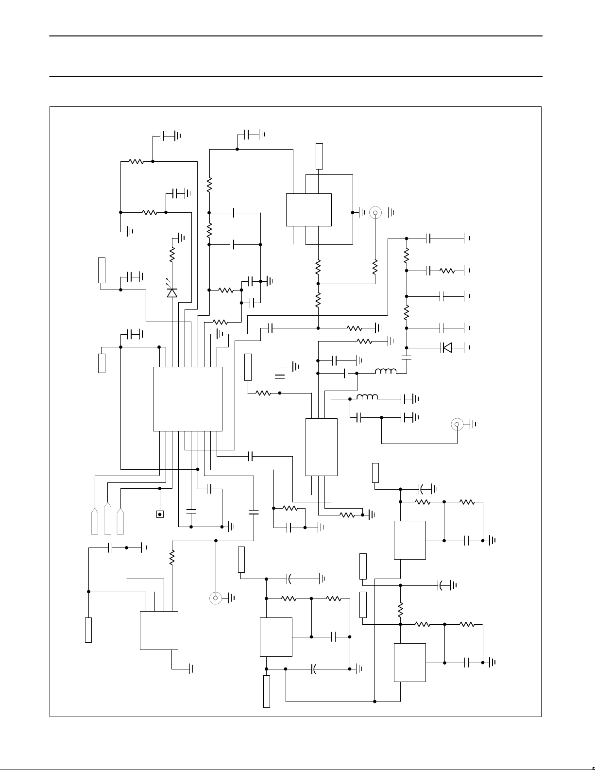
Components values shown as:
PHS (PDC1500)
R21
R24
18k (360k)
36k (56k)
R22
10k (51k)
C35
100nF
C29
100nF
R25
C34
UL
VDDA
C28
100nF
LED
D1
R20
560R
C21
100nF
VDD
R26
NL
R23
10k (13k)
C30
NL
C31
3.9nF (10nF)
C32
390pF (1nF)
C33
150pF (18pF)
G2
VCO
M
G
P
C
G
B
1
2
3
6
5
4
VOSC
MQE530-1667MHz
R14
18R
R15
18R
R16
18R
JP3
RF-OUT
R17
10k
C26
150nF
R19
8.2k
C27
10nF
C24
8.2pF
R18
9.1k
U1
123456789
10
201918171615141312
11
CLK
DATA
STB
VSSD
RF IN+
RF IN–
VCCP
REF IN
RA
AUXIN
VDD
TEST
LOCK
RF
RN
VDDA
PHP
PHI
VSSA
PHA
SA8025
JP1
CLK
DATA
STB
VOSC
G1
5
432
1
VCC
NC
GND
OUT
TEW-TCXO
19.2MHz
C8
100nF
IN-REF
R8
J3
TP
C9
1nF
C10
1nF
C11
10nF
5V
VAUX
C13
1nF
VAUX
R11
27R
C22
C15
1nF
R13
51R
C20
12pF
R12
10k
C18
8.2pF
L1
180nH
C19
1nF
L2
750nH
3.9pF
C23
15pF
VR!
BB215
JP2
AUX-OUT
123
4
876
5
U5
NE602A
INP-A
INP-B
GND
OUTA
VCC
OSCE
OSCB
OUTB
C16
18pF
C17
56pF
+
C3
4.7uF
10V
C12
100nF
R10
10k
R9
130k
3V
VDD
+
C7
4.7uF
10V
R7
4.3k
C6
100nF
R6
3.3k
3
2
1
U3
LM317LZ
IN OUT
ADJ
+
C5
47uF
10V
4V
VOSC
5V
VDDAR50
R3
3.3k
R4
4.3k (9.1k)
U2
LM317LZ
3 2
1
ADJ
IN
C4
100nF
OUT
8V
POWER
R1
3.3k
U3
LM317LZ
3 2
1
ADJ
IN
OUT
+
C1
4.7uF
10V
R2
9.1k
C2
100nF
GND
(MQE060-1619MHz)
SR00577
Figure 26. SA8025ADK Application Circuit
Page 22
Philips Semiconductors Product specification
SA8025A1.8GHz low-voltage Fractional-N synthesizer
1996 Oct 15
22
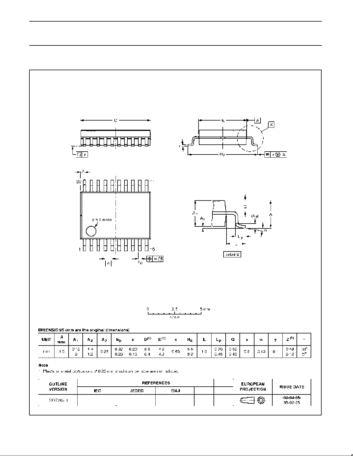
SSOP20: plastic shrink small outline package; 20 leads; body width 4.4 mm SOT266-1
Page 23

Philips Semiconductors Product specification
SA8025A1.8GHz low-voltage Fractional-N synthesizer
1996 Oct 15
23
Philips Semiconductors and Philips Electronics North America Corporation reserve the right to make changes, without notice, in the products,
including circuits, standard cells, and/or software, described or contained herein in order to improve design and/or performance. Philips
Semiconductors assumes no responsibility or liability for the use of any of these products, conveys no license or title under any patent, copyright,
or mask work right to these products, and makes no representations or warranties that these products are free from patent, copyright, or mask
work right infringement, unless otherwise specified. Applications that are described herein for any of these products are for illustrative purposes
only. Philips Semiconductors makes no representation or warranty that such applications will be suitable for the specified use without further testing
or modification.
LIFE SUPPORT APPLICATIONS
Philips Semiconductors and Philips Electronics North America Corporation Products are not designed for use in life support appliances, devices,
or systems where malfunction of a Philips Semiconductors and Philips Electronics North America Corporation Product can reasonably be expected
to result in a personal injury. Philips Semiconductors and Philips Electronics North America Corporation customers using or selling Philips
Semiconductors and Philips Electronics North America Corporation Products for use in such applications do so at their own risk and agree to fully
indemnify Philips Semiconductors and Philips Electronics North America Corporation for any damages resulting from such improper use or sale.
This data sheet contains preliminary data, and supplementary data will be published at a later date. Philips
Semiconductors reserves the right to make changes at any time without notice in order to improve design
and supply the best possible product.
Philips Semiconductors
811 East Arques Avenue
P.O. Box 3409
Sunnyvale, California 94088–3409
Telephone 800-234-7381
DEFINITIONS
Data Sheet Identification Product Status Definition
Objective Specification
Preliminary Specification
Product Specification
Formative or in Design
Preproduction Product
Full Production
This data sheet contains the design target or goal specifications for product development. Specifications
may change in any manner without notice.
This data sheet contains Final Specifications. Philips Semiconductors reserves the right to make changes
at any time without notice, in order to improve design and supply the best possible product.
Philips Semiconductors and Philips Electronics North America Corporation
register eligible circuits under the Semiconductor Chip Protection Act.
Copyright Philips Electronics North America Corporation 1996
All rights reserved. Printed in U.S.A.
 Loading...