

Page 1

Philips Semiconductors RF Communications Products Product specification
SA702
Divide by: 64/65/72 triple modulus low power
ECL prescaler
2
June 17, 1993 853-1709 10044
DESCRIPTION
The SA702 triple modulus (Divide By
64/65/72) low power ECL prescaler is used in
synthesizer systems to achieve low phase
lock time, broad operating range, high
reference frequency and small frequency
step sizes. The minimum supply voltage is
2.7V and is compatible with the CMOS
UMA1005 synthesizer from Philips and other
logic circuits. The low supply current allows
application in battery operated low-power
equipment. Maximum input signal frequency
is 1.1GHz for cellular and other land mobile
applications. There is no lower frequency
limit due to a fully static design. The circuit is
implemented in ECL technology on the
QUBiC process. The circuit will be available
in an 8-pin SO package with 150 mil package
width and in 8-pin dual in-line plastic
package.
FEATURES
•Low voltage operation
•Low current consumption
•Operation up to 1.1GHz
•ESD hardened
APPLICATIONS
•Cellular phones
•Cordless phones
•RF LANs
•Test and measurement
•Military radio
•VHF/UHF mobile radio
•VHF/UHF hand-held radio
PIN CONFIGURATION
IN
V
C
C
MC2
OUT
IN
MC1
1
2
3
4 5
6
78GND
OUT
N, D Package
ORDERING INFORMATION
DESCRIPTION TEMPERATURE RANGE ORDER CODE DWG #
8-Pin Plastic Dual In-Line Package (DIP) -40 to +85°C SA702N 0404B
8-Pin Plastic Small Outline (SO) package (Surface-mount) -40 to +85°C SA702D 0174C
ABSOLUTE MAXIMUM RATINGS
SYMBOL PARAMETER RATING UNITS
V
CC
Supply voltage -0.3 to +7.0 V
V
IN
Voltage applied to any other pin -0.3 to (VCC + 0.3) V
I
O
Output current 10 mA
T
STG
Storage temperature range -65 to +125 °C
T
A
Operating ambient temperature range -55 to +125 °C
θ
JA
Thermal impedance D package
N package
158
108
°C/W
Page 2
Philips Semiconductors RF Communications Products Product specification
SA702
Divide by: 64/65/72 triple modulus low power
ECL prescaler
June 17, 1993
3
BLOCK DIAGRAM
D
Q
D
Q Q
D
Q Q
D
Q
D
Q Q
D
Q
D
Q
D
Q
MODULUS CONTROL
LOGIC
OUT
IN
IN
MC1
MC2
OUT
Page 3
Philips Semiconductors RF Communications Products Product specification
SA702
Divide by: 64/65/72 triple modulus low power
ECL prescaler
June 17, 1993
4
DC ELECTRICAL CHARACTERISTICS
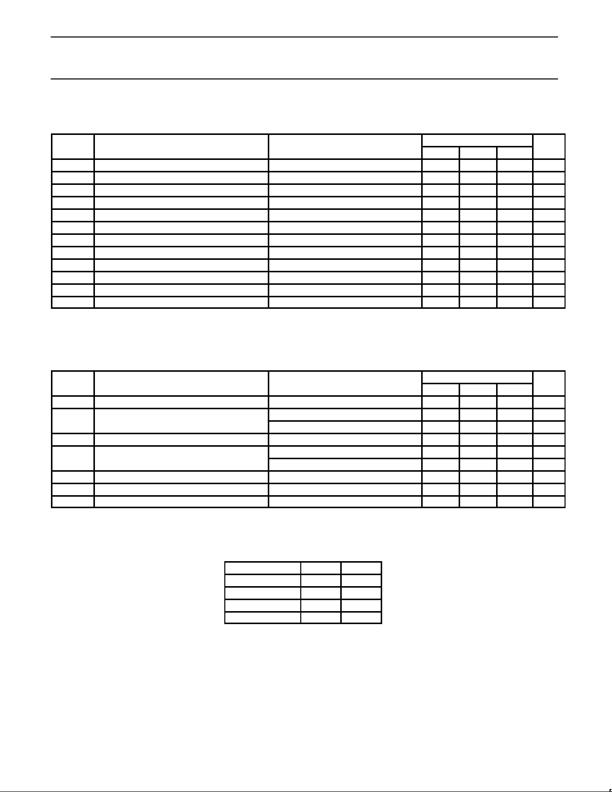
The following DC specifications are valid for TA = 25°C and VCC = 3.0V; unless otherwise stated. Test circuit Figure 1.
SYMBOL
PARAMETER TEST CONDITIONS LIMITS UNITS
MIN TYP MAX
V
CC
Power supply voltage range fIN = 1GHz, input level = 0dBm 2.7 6.0 V
I
CC
Supply current No load 4.5 mA
V
OH
Output high level I
OUT
= 1.2mA VCC-1.4 V
V
OL
Output low level VCC-2.6 V
V
IH
MC1 input high threshold 2.0 V
CC
V
V
IL
MC1 input low threshold –0.3 0.8 V
V
IH
MC2 input high threshold 2.0 V
CC
V
V
IL
MC2 input low threshold –0.3 0.8 V
I
IH
MC1 input high current V
MC1
= VCC = 6V 0.1 50 µA
I
IL
MC1 input low current V
MC1
= 0V, VCC = 6V –100 –30 µA
I
IH
MC2 input high current V
MC2
= VCC = 6V 0.1 50 µA
I
IL
MC2 input low current V
MC2
= 0V, VCC = 6V –100 –30 µA
AC ELECTRICAL CHARACTERISTICS
These AC specifications are valid for fIN = 1GHz, input level = 0dBm, VCC = 3.0V and TA = 25°C; unless otherwise stated. Test circuit Fig. 1.
SYMBOL
PARAMETER TEST CONDITIONS LIMITS UNITS
MIN TYP MAX
V
IN
Input signal amplitude
1
1000pF input coupling 0.05 2.0 V
P-P
f
IN
Input signal frequency Direct coupled input
2
0 1.1 GHz
1000pF input coupling 1.1 GHz
R
ID
Differential input resistance DC measurement 5 kΩ
V
O
Output voltage VCC = 5.0V 1.6 V
P-P
VCC = 3.0V 1.2 V
P-P
t
S
Modulus set-up time
1
5 ns
t
H
Modulus hold time
1
0 ns
t
PD
Propagation time 10 ns
NOTES:
1. Maximum limit is not tested, however, it is guaranteed by design and characterization.
2. For f
IN
< 50MHz, minimum input slew rate of 32V/µs is required.
DESCRIPTION OF OPERATION
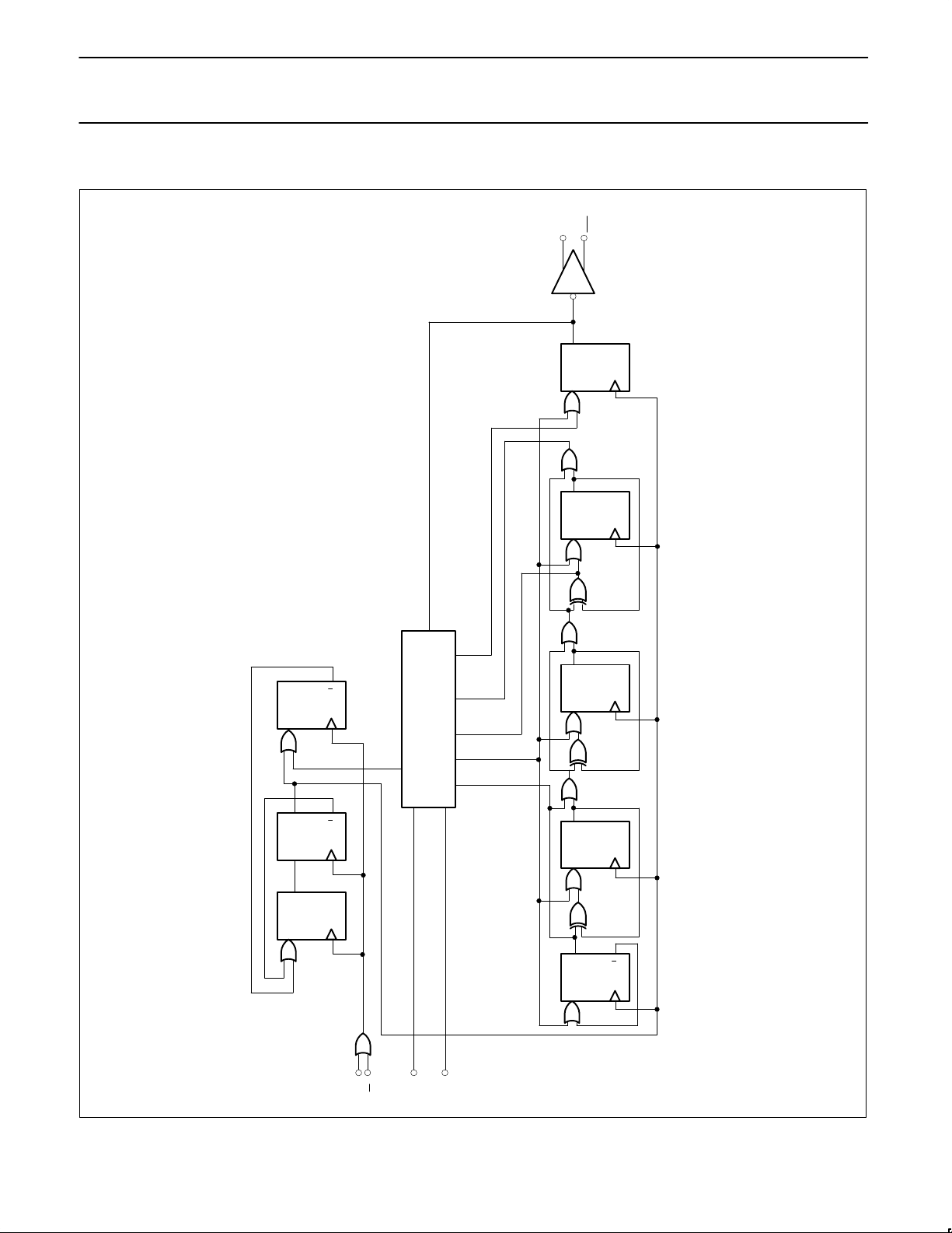
The SA702 comprises a frequency divider
circuit implemented using a divide by 4 or 5
synchronous prescaler followed by a 5 stage
synchronous counter, see BLOCK
DIAGRAM. The normal operating mode is for
MC1 (Modulus Control) to be set high and
MC2 input to be set low in which case the
circuit comprises a divide by 64. For divide
by 65 the MC1 singal is forced low, causing
the prescaler circuit to switch into divide by 5
operation for the last cycle of the
synchronous counter. For divide by 72, MC2
is set high configuring the prescaler to divide
by 4 and the counter to divide by 18. A truth
table for the modulus values is given below:
Table 1.
Modulus MC1 MC2
64 1 0
65 0 0
72 0 1
72 1 1
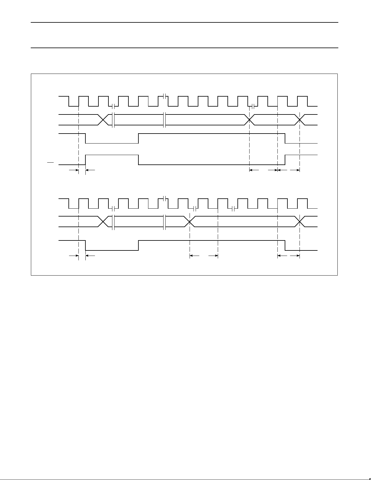
For minimization of propagation delay effects,
the second divider circuit is synchronous to
the divide by 4/5 stage output.
The prescaler input is positive edge sensitive,
and the output at the final count is a falling
edge with propagation delay t
PD
relative to
the input. The rising edge of the output
occurs at the count 32 with delay t
PD
.
The MC1 and MC2 inputs are TTL
compatible threshold inputs operating at a
reduced input current. CMOS and low
voltage interface capability are allowed.
The prescaler input is differential and ECL
compatible. The output is differential ECL
compatible.
Page 4
Philips Semiconductors RF Communications Products Product specification
SA702
Divide by: 64/65/72 triple modulus low power
ECL prescaler
June 17, 1993
5
AC TIMING CHARACTERISTICS
(00) (XX) (10)
64 65 1 32 63 64 1COUNT
IN
MC (2:1)
OUT
64 65 1 32 71 72 1COUNT
IN
MC
OUT
t
P
D
t
S
t
H
SWITCH FROM /65 TO /64
t
P
D
t
S
t
H
SWITCH FROM /65 TO /72
(00) (XX) (01)
OUT
62 63 64
Page 5
Philips Semiconductors RF Communications Products Product specification
SA702
Divide by: 64/65/72 triple modulus low power
ECL prescaler
June 17, 1993
6
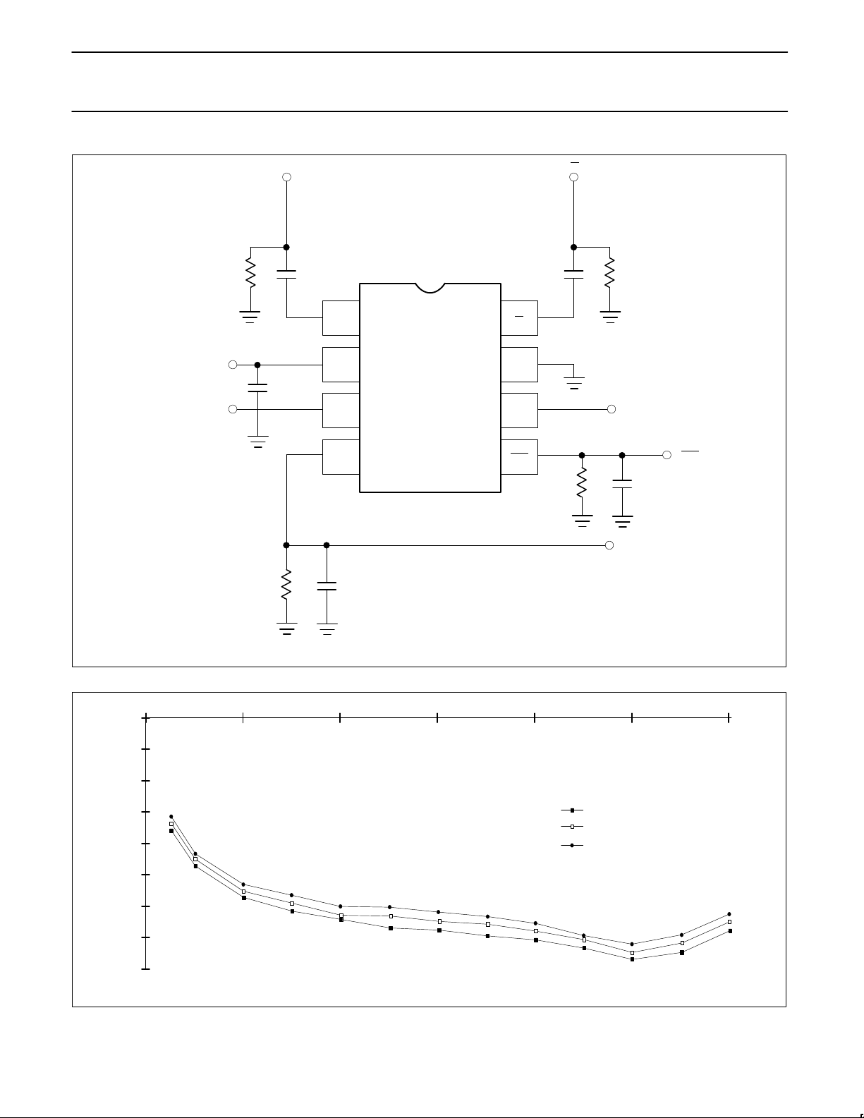
Figure 1. SA702 Test Circuit
IN
V
CC
MC2
OUT OUT
MC1
GND
IN
50Ω 50Ω
IN IN
C1
1000pF
C2
1000pF50Ω
R1
50Ω
R2
MC1
V
CC
MC2
2.2kΩ
R3
C4
5pF
OUT
C3
0.1µF
2.2kΩ
R4
C5
5pF
OUT
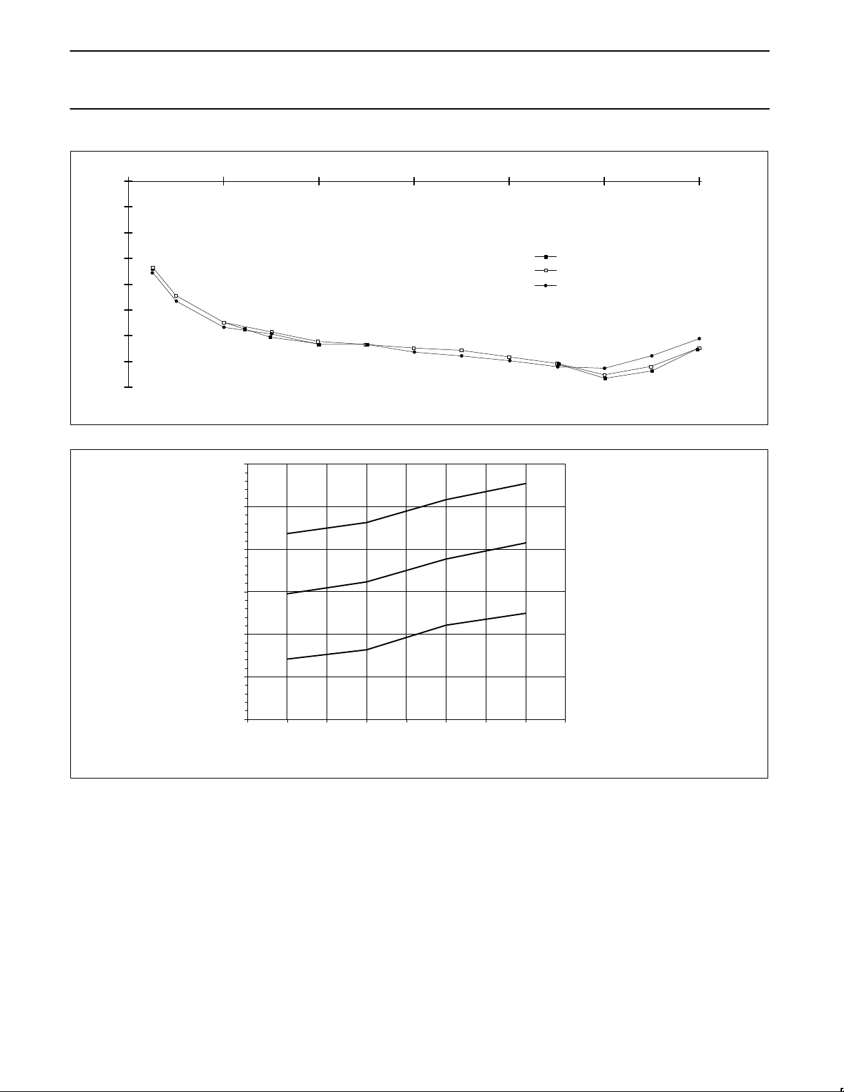
Figure 2. Minimum Input Power vs Frequency and Temperature
0
–5
–10
–15
–20
–25
–30
–35
–40
200 400 600 800 1000 1200
25°C
MINIMUM INPUT POWER (dBm)
FREQUENCY (MHz)
–40°C
85°C
V
CC
= 3.0V
Page 6
Philips Semiconductors RF Communications Products Product specification
SA702
Divide by: 64/65/72 triple modulus low power
ECL prescaler
June 17, 1993
7
Figure 3. Minimum Input Power vs Frequency and V
CC
0
–5
–10
–15
–20
–25
–30
–35
–40
200 400 600 800 1000 1200
TA = 25°C
2.7V
3.0V
6.0V
MINIMUM INPUT POWER (dBm)
FREQUENCY (MHz)
Figure 4. Supply Current vs Supply Voltage and Temperature With No Load
VCC (V)
6
5.5
5
4.5
4
3.5
3
2.7 3 6 7
I (mA)
CC
85°C
–40°C
25°C
Page 7
Philips Semiconductors RF Communications Products Product specification
SA702
Divide by: 64/65/72 triple modulus low power
ECL prescaler
June 17, 1993
8
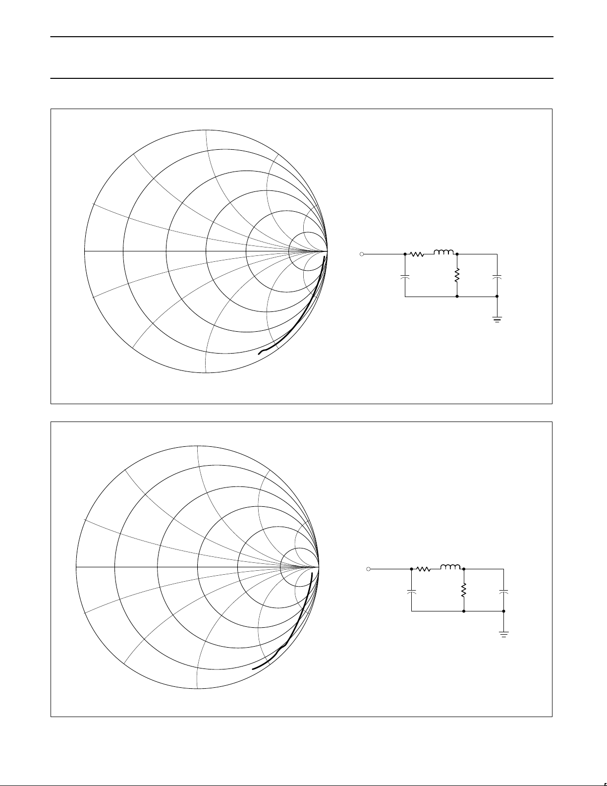
Figure 5. Typical N Package Input Impedance
R3
L4
R1
C2 C1
INPUT
4Ω
6nH
0.4pF
0.9pF
3000Ω
0
j0.2
j0.5
j1
j2
j5
–j5
–j2
–j1
–j0.5
–j0.2
0.2 0.5 1 2
5
V
CC
= 3V
TA = 25°C
EQUIVALENT INPUT IMPEDANCE
50
300
600
900
1200
Figure 6. Typical D Package Input Impedance
R3
L4
R1
C2 C1
INPUT
2Ω
3nH
0.2pF
0.9pF
3000Ω
0
j0.2
j0.5
j1
j2
j5
–j5
–j2
–j1
–j0.5
–j0.2
0.2 0.5 1 2
5
V
CC
= 3V
T
A
= 25°C
EQUIVALENT INPUT IMPEDANCE
50
300
600
900
1200
 Loading...