

Page 1

INTEGRATED CIRCUITS
SA5223
Wide dynamic range AGC
transimpedance amplifier (150MHz)
Product specification 1995 Oct 24
IC19 Data Handbook
Philips
Semiconductors
Page 2
Philips Semiconductors Product specification
SA5223Wide dynamic range AGC transimpedance amplifier(150MHz)
DESCRIPTION
The SA5223 is a wide-band, low-noise transimpedance amplifier
with differential outputs, incorporating AGC and optimized for signal
recovery in wide-dynamic-range fiber optic receivers, such as
SONET. The part is also suited for many other RF and fiber optic
applications as a general purpose gain block.
The SA5223 is the first AGC amplifier to incorporate internal AGC
loop hold capacitor, therefore, no external components are required.
The internal AGC loop enables the SA5223 to effortlessly handle
bursty data over a range of nA to mA of signal current, positive
direction (sinking) only.
FEA TURES
•Extremely low noise:
1.17pA
Hz
•Single 5V supply
•Low supply current: 22mA
•Large bandwidth: 150MHz
•Differential outputs
•Internal hold capacitor
•Low input/output impedances
•High power-supply-rejection ratio: 55dB
•Tight transresistance control
•High input overload: 4mA
•2000V HBM ESD protection
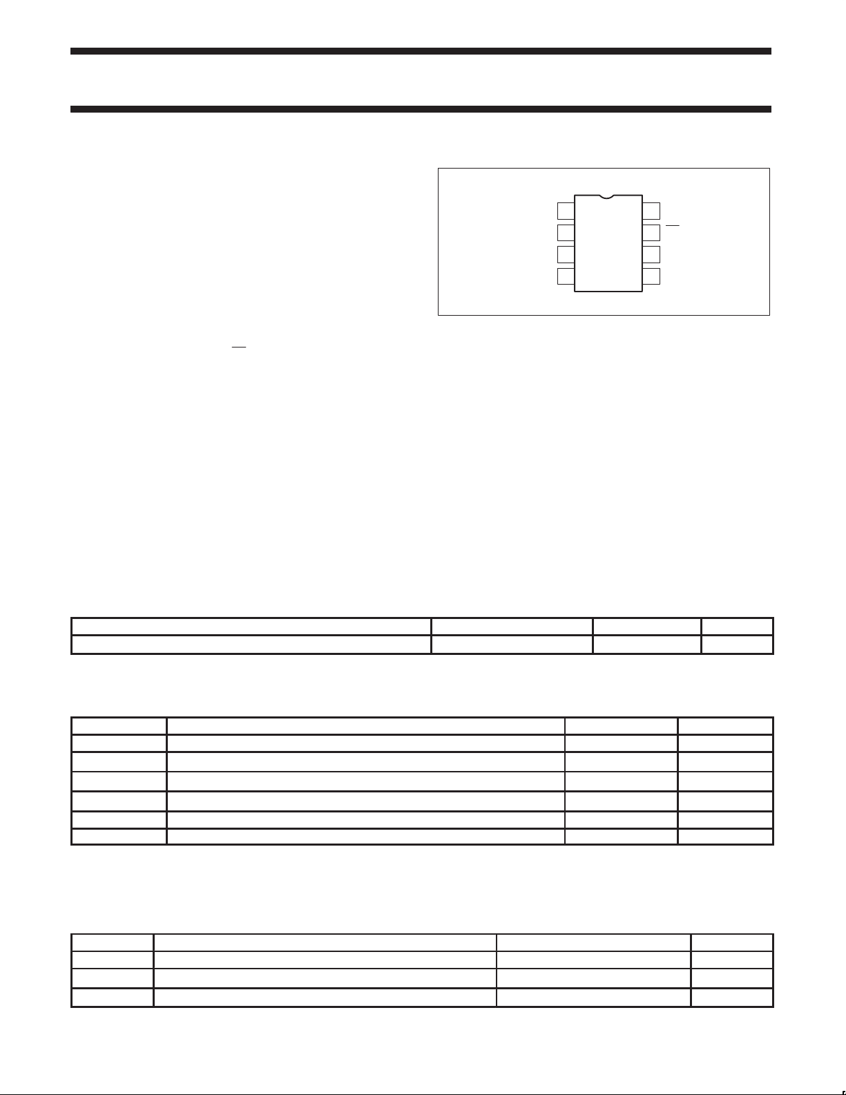
PIN DESCRIPTION
D Package
GND
GND
GND
1
3
2
1
3
IN
4
4
V
8
OUT
7
6
OUT
5
GND
SD00369
CC
2
APPLICATIONS
•OC3 SONET preamp (see AN1431 for detailed analysis
•Current-to-voltage converters
•Wide-band gain block
•Medical and scientific instrumentation
•Sensor preamplifiers
•Single-ended to differential conversion
•Low noise RF amplifiers
•RF signal processing
ORDERING INFORMATION
DESCRIPTION TEMPERATURE RANGE ORDER CODE DWG #
8-Pin Plastic Small Outline
For unpackaged die please contact factory.
-40 to +85°C
SA5223D SOT96-1
ABSOLUTE MAXIMUM RATINGS
SYMBOL PARAMETER RATING UNITS
V
CC
T
A
T
J
T
STG
P
D
I
INMAX
NOTE:
1. Maximum power dissipation is determined by the operating ambient temperature and the thermal resistance θ
6.2mW/
°C above 25°C.
Power supply voltage 6 V
Ambient temperature range -40 to +85
Junction temperature range -55 to +150
Storage temperature range -65 to +150
Power dissipation TA = 25oC (still air)
Maximum input current 5 mA
1
0.78 W
= 158oC/W. Derate
JA
RECOMMENDED OPERATING CONDITIONS
SYMBOL PARAMETER RATING UNITS
V
CC
T
A
T
J
Power supply voltage 4.5 to 5.5 V
Ambient temperature range: SA grade -40 to +85
Junction temperature range: SA grade -40 to +105
°C
°C
°C
°C
°C
1995 Oct 24 853-1816 15939
2
Page 3
Philips Semiconductors Product specification
SYMBOL
PARAMETER
TEST CONDITIONS
UNIT
SYMBOL
PARAMETER
TEST CONDITIONS
UNIT
idth (ref
t)
C
S
1F
T
SA5223Wide dynamic range AGC transimpedance amplifier(150MHz)
DC ELECTRICAL CHARACTERISTICS
Typical data and Min and Max limits apply at TA = 25°C, and VCC = +5V, unless otherwise specified.
SA5223
Min Typ Max
V
V
V
I
I
OMAX
NOTE: Standard deviations are estimated from design simulations to represent manufacturing variations over the life of the product.
AC ELECTRICAL CHARACTERISTICS
Typical data and Min and Max limits apply at TA = 25°C and VCC = +5V, unless otherwise specified.
R
R
R
R
f
3dB
R
C
C
∆R/∆V Transresistance power supply sensitivity V
∆R/∆T
PSRR Power supply rejection ratio (change in VOS) DC Tested, ∆VCC = ±0.5V –55 dB
PSRR Power supply rejection ratio
V
OLMAX
dR
I
INMAX
tr, t
NOTES:
1. Does not include Miller-multiplied capacitance of input device.
2. Noise performance measured differential. Single-ended output noise is higher due to CM noise.
3. PSRR is output referenced and is circuit board layout dependent at higher frequencies. For best performance use a RF filter in VCC line.
4. This implies that the SA5223 gain will change 1dB (10%) in the absence of data for 1ms (i.e., can handle bursty data without degrading Bit
Error Rate (BER) for 100,000 cycles at 100MHz).
Input bias voltage 1.3 1.55 1.8 V
IN
Output bias voltage 2.9 3.2 3.5 V
±
O
Output offset voltage (V
OS
Supply current 15 22 29 mA
CC
PIN6
- V
) -200 80 +200 mV
PIN7
Output sink/source current 1.5 2 mA
SA5223
Min Typ Max
Transresistance (differential output)
T
Transresistance
T
(single-ended output)
Output resistance
O
(differential output)
Output resistance
O
(single-ended output)
DC tested, RL = ∞, IIN = 0-1µA
DC tested, RL = ∞, IIN = 0-1µA
DC tested 140 Ω
DC tested 70 Ω
90 125 160 kΩ
45 62.5 80 kΩ
Bandwidth (-3dB) Test Circuit 1 110 150 MHz
Input resistance DC tested 250
IN
Input capacitance
IN
Input capacitance including Miller multiplied
INT
capacitance
Transresistance ambient temperature sensitivity
RMS noise current spectral density (referred
I
IN
to input)
2
Integrated RMS noise current over the bandw
=
p
= 0.
I
T
1
erred to inpu
0.7
4.0
= V
CC1
∆TA = T
= 5 ±0.5V 3 %/V
CC2
A MAX
- T
A MIN
0.09
Test Circuit 2, f = 10MHz 1.17
Test circuit 2,
∆f = 50MHz
7
∆f = 100MHz 12
∆f = 150MHz 16
∆f = 50MHz 8
CS = 0.4pF ∆f = 100MHz 13
∆f = 150MHz 18
3
f = 1.0MHz, Test Circuit 3 –20 dB
Maximum differential output AC voltage Ii = 0–2mA peak AC 800 mV
T
AGC loop time constant parameter
dt
Maximum input amplitude for output duty
cycle of 50 ±5%
Output rise and fall times 10 – 90% 2.2 ns
f
t
Group delay f = 10MHz 2.2 ns
D
4
10µA to 20µA steps 1 dB/ms
Test circuit 4 +2 mA
Ω
pF
pF
%/oC
pA Hz
nA
1995 Oct 24
3
Page 4
Philips Semiconductors Product specification
SA5223Wide dynamic range AGC transimpedance amplifier(150MHz)
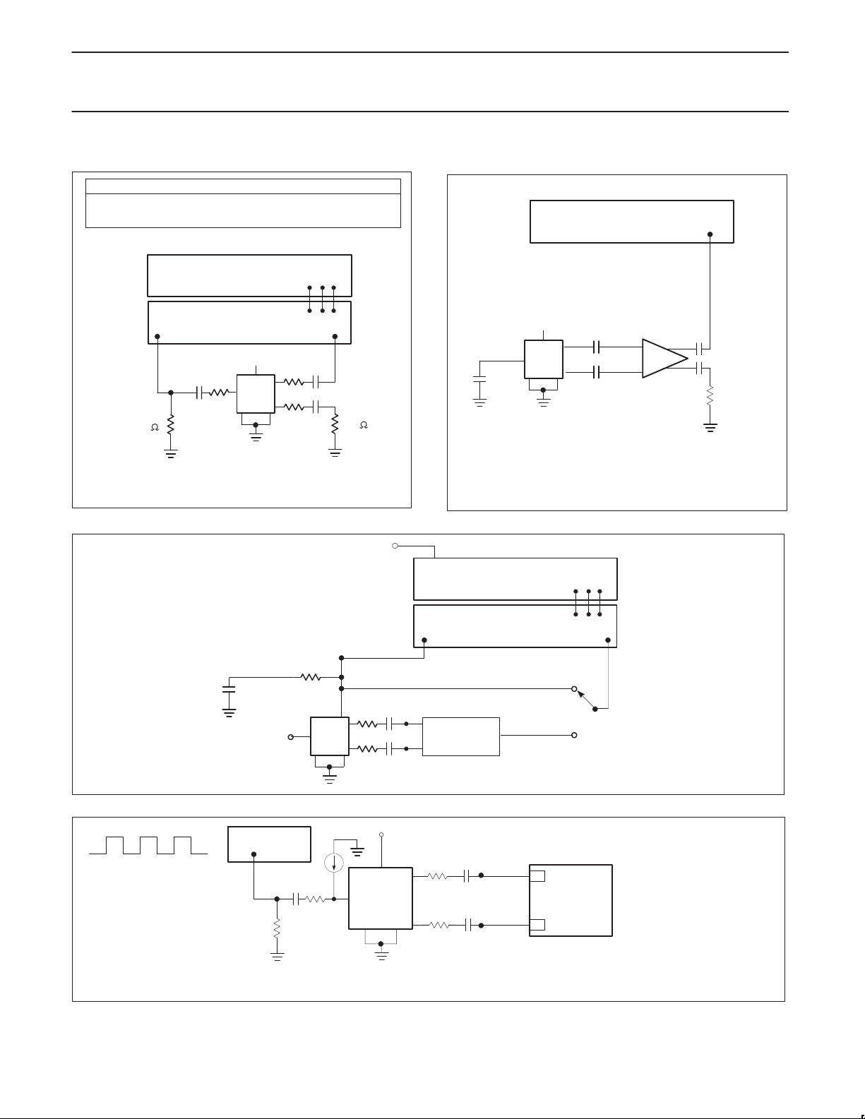
TEST CIRCUITS
SINGLE-ENDED
R
+ 12.4 @ S21@ RIN,RIN+ 1k ) R
TSE
NETWORK ANALYZER
S-PARAMETER TEST SET
PORT1 PORT2
Z
= 50Ω
O
0.1uF
IN DUT
R=1k
GND
50
1
V
CC
500
OUT
500
OUT
GND
2
.1uF
.1uF
INSS
[ 1250
= 50Ω
Z
O
50
SPECTRUM ANALYZER
V
CC
OUT
IN DUT
OUT
GND
C
S
1
GND
.1µF
.1µF
2
50Ω
1.0µF
NE5209
1.0µF
50Ω
50% DUTY CYCLE
Test Circuit 1: Bandwidth
50Ω
0.1uF
NC
GND
PULSE GEN
OFFSET
0.1uF
50Ω
SD00370
1
V
CC
OUT
IN DUT
OUT
GND
5V
.1uF
.1uF
100Ω
2
BAL.
BIAS TEE
NETWORK ANALYZER
S-PARAMETER TEST SET
PORT1 PORT2
NHO300HB
Test Circuit 3: PSRR
5V
.1µF
500Ω
OUT
DUT
GND
IN
OUT
1
GND
2
500Ω
.1µF
1kΩ
Test Circuit 4: Duty Cycle Distortion
Test Circuit 2: Noise
CAL
50Ω
UNBAL.
A
ZO = 50Ω
OSCILLOSCOPE
B
Z
= 50Ω
O
Meaurement done using
differential wave forms
SD00373
SD00371
TRANSFORMER
CONVERSION
LOSS = 9dB
SD00372
1995 Oct 24
4
Page 5

Philips Semiconductors Product specification
SA5223Wide dynamic range AGC transimpedance amplifier(150MHz)
V
GND
G1
IN
1
2
3
NC NC
NC
8
7
6
CC
OUT
OUTB
PAD CENTER LOCATIONS
X(mm) Y(mm)
GND1 -0.400 -0.053
IN -0.400 -0.223
GND2 +0.400 -0.342
OUT +0.400 -0.046
OUTB +0.400 +0.154
V
+0.400 +0.380
CC
DIE SIZE
X(mm) Y(mm)
1.08 1.32
GND
4
Figure 1. SA5223 Bonding Diagram
Die Sales Disclaimer
Due to the limitations in testing high frequency and other parameters
at the die level, and the fact that die electrical characteristics may
shift after packaging, die electrical parameters are not specified and
die are not guaranteed to meet electrical characteristics (including
temperature range) as noted in this data sheet which is intended
only to specify electrical characteristics for a packaged device.
All die are 100% functional with various parametrics tested at the
wafer level, at room temperature only (25°C), and are guaranteed to
be 100% functional as a result of electrical testing to the point of
wafer sawing only. Although the most modern processes are
utilized for wafer sawing and die pick and place into waffle pack
5
G2
SD00507
carriers, it is impossible to guarantee 100% functionality through this
process. There is no post waffle pack testing performed on
individual die.
Since Philips Semiconductors has no control of third party
procedures in the handling or packaging of die, Philips
Semiconductors assumes no liability for device functionality or
performance of the die or systems on any die sales.
Although Philips Semiconductors typically realizes a yield of 85%
after assembling die into their respective packages, with care
customers should achieve a similar yield. However, for the reasons
stated above, Philips Semiconductors cannot guarantee this or any
other yield on any die sales.
1995 Oct 24
5
Page 6

Philips Semiconductors Product specification
SA5223Wide dynamic range AGC transimpedance amplifier(150MHz)
DOUT
DOUT
C12
0.1uF
Ω
R10
130
C11
0.1uF
Ω
R5
5
+3.2V
Ω
R7
82
+5V
Ω
R6
130
C13
0.1uF
R12
R11
Ω
1.8k
Ω
3k
+5V
Ω
R9
82
Ω
R8
5
BOTTOM PLANE
TOP PLANE
16151413121110
VccE
VSET
VREF
D_OUT
D_OUT
U2
CAZN
CAZP
GNDA
D_IN
D_IN
1
2
3
4
5
C5
0.1uF
C6
0.1uF
C4
4.7pF
R3
120Ω
8
7
6
C3
Ω
R2
0
0.1uF
Vcc
OUT
OUT
ST
GND_E
VccACFJAM
6
7
C8
0.1uF
R4
120Ω
5
GND2
C8
9
ST
8
0.1uF
NE5224
C9
0.1uF
L2
10uH
C10
4.7uF
+
+5V
1995 Oct 24
+5V
C1
C2
0.1uF
0.1uF
U1
1
D1*
GND3
GND1INGND4
2
3
SA5223
4
L1
10uH
Ω
R1
100
Figure 2. SONET Test Board — 155Mb/s (1300nm)
6
λ
ABB HAFO 1.5GHz PIN DIODE
*D1: 1A358 – = 1300nm
ANALOG GND
SD00521
DIGITAL GND
Page 7

Philips Semiconductors Product specification
SA5223Wide dynamic range AGC transimpedance amplifier(150MHz)
FO11000
SA5223/5224
GND
+5V
SONET – 155MB/s
C3
R2
L1
C1
R1
C2
U1
D1
GND
+5V
R3
R4
L2
C10
GND
U2
DoutDout
C11
C4
C9
C8
C6
C7
C5
C13
R11
R5
R8
C12
R7
R9
R10
R6
GND
R12
1995 Oct 24
TOP VIEW BOTTOM VIEW
SD00522
Figure 3. SA5223 Board Layout (NOT ACTUAL SIZE)
7
Page 8

Philips Semiconductors Product specification
SA5223Wide dynamic range AGC transimpedance amplifier(150MHz)
28.00
26.00
24.00
22.00
20.00
SUPPLY CURRENT (mA)
18.00
16.00
-50 -25 0 25 50 75 100
TEMPERATURE (°C)
Figure 4. SA5223 ICC vs Temperature
1.900
1.800
1.700
1.600
1.500
1.400
SUPPLY CURRENT (mA)
1.300
1.200
-50 -25 0 25 50 75 100
Figure 5. SA5223 Input V
TEMPERATURE (°C)
BIAS
vs Temperature
VCC = 5.5V
V
= 5.0V
CC
= 4.5V
V
CC
VCC = 5.5V
V
= 5.0V
CC
= 4.5V
V
CC
SD00528
SD00527
100
90
80
70
OS
V (mV)
60
50
40
VOS = (IIN = 0) = V
RL = INFINITY
-50 -25 0 25 50 75 100
– V
OUT
OUT
TEMPERATURE (°C)
VCC = 5.5V
VCC = 4.5V
Figure 7. SA5223 Output VOS vs Temperature
3.500
3.400
3.300
3.200
OUT
V (V)
3.100
3.000
2.900
0123456
RL = INFINITY
V
= 5.0V, Temperature = 25°C
CC
DC INPUT CURRENT (µA)
8910
7
Figure 8. SA5223 Output Voltage vs DC Input Current
(for small input current)
V
CC
SD00530
V
OUT
V
OUT
SD00531
= 5.0V
3.800
3.600
3.400
BIAS
3.200
3.000
OUTPUT V (V)
2.800
2.600
Figure 6. SA5223 Output V
1995 Oct 24
VCC = 5.5V
= 5.0V
V
CC
V
= 4.5V
CC
-50 -25 0 25 50 75 100
TEMPERATURE (°C)
vs Temperature
BIAS
SD00529
4.200
4.000
3.800
3.600
3.400
3.200
3.000
OUT
V (V)
2.800
2.600
2.400
2.200
2.000
RL = INFINITY
VCC = 5.0V, Temperature = 25°C
1 10 100 1000 10000
DC INPUT CURRENT (µA LOG)
V
OUT
V
OUT
SD00532
Figure 9. SA5223 Output Voltage vs DC Input Current
(for large input current)
8
Page 9

Philips Semiconductors Product specification
SA5223Wide dynamic range AGC transimpedance amplifier(150MHz)
0.350
0.300
0.250
0.200
0.150
OD
V (V)
0.100
0.050
0.000
0123456
RL = INFINITY
VCC = 5.0V, Temperature = 25°C
V
= V
– V
OD
OUT
DC INPUT CURRENT (µA)
OUT
– V
OS
7
Figure 10. SA5223 Differential Output vs DC I
(for small input current)
1.800
1.600
RL = INFINITY
1.400
VCC = 5.0V, Temperature = 25°C
1.200
1.000
0.800
OD
V (V)
0.600
0.400
0.200
0.000
= V
– V
V
OD
OUT
1 10 100 1000 10000
– V
OUT
OS
DC INPUT CURRENT (µA, LOG)
Figure 11. SA5223 Differential Output vs DC I
8910
SD00533
IN
SD00534
IN
1000
85°C
100
10
Ω
RT (K , LOG)
1
0
25°C
-40°C
1 10 100 1000 10000
DC INPUT CURRENT (µA LOG)
RL = INFINITY
VCC = 5.0V
Temperature = -40, 25, 85°C
RT = V
/ I
OD
IN
Figure 13. SA5223 Differential RT vs DC I
(for large input current)
160
140
120
100
Ω
80
V
RT (K )
60
40
20
0
0123456
CC
= 4.5V
V
= 5.5V
CC
V
CC
DC INPUT CURRENT (µA)
= 5.0V
RL = INFINITY
VCC = 5.0V
Temperature = 25°C
RT = V
/ I
OD
78910
Figure 14. SA5223 Differential RT vs DC I
(for small input current)
SD00536
IN
IN
SD00537
IN
160
140
120
-40°C
100
Ω
80
RT (K )
60
40
20
0
0123456
85°C
25°C
DC INPUT CURRENT (µA)
Figure 12. SA5223 Differential RT vs DC I
(for small input current)
1995 Oct 24
RL = INFINITY
VCC = 5.0V
Temperature = -40, 25, 85°C
RT = V
/ I
OD
IN
78910
IN
SD00535
1000
RL = INFINITY
100
25°C
10
Ω
RT (K , LOG)
1
0
1 10 100 1000 10000
DC INPUT CURRENT (µA LOG)
Figure 15. SA5223 Differential RT vs DC I
VCC = 4.5, 5.0, 5.0V
Temperature = 25°C
/ I
RT = V
OD
IN
85°C
-40°C
IN
SD00538
(for large input current)
9
Page 10

Philips Semiconductors Product specification
SA5223Wide dynamic range AGC transimpedance amplifier(150MHz)
16
14
12
10
8
6
21
S (dB)
4
2
0
-2
-4
1 10 100 300
VCC = 5.0V
SINGLE-ENDED OUTPUT
FREQUENCY (MHz)
Figure 16. Insertion Gain vs Frequency
16
14
12
10
8
21
6
S (dB)
4
2
0
-2
-4
1 10 100 300
TEMPERATURE = 25°C
SINGLE-ENDED OUTPUT
FREQUENCY (MHz)
VCC = 5.5V
VCC = 5.0V
V
= 4.5V
CC
Figure 17. Insertion Gain vs Frequency
-40°C
0°C
25°C
70°C
85°C
SD00539
SD00540
9
8
7
6
5
4
3
2
21
S GROUP DELAY (ns)
1
0
-1
START = 1MHz STOP = 200MHz
SINGLE-ENDED OUTPUT
TEMPERATURE = 25°C
VCC = 5.0V
FREQUENCY (MHz, LINEAR)
SD00541
Figure 18. Group Delay vs Frequency
10.0
9.0
VCC = 5.0V
8.0
Temperature = 25°C
7.0
√
INPUT NOISE (PA/ Hz)
CS = 0pF
6.0
5.0
4.0
3.0
2.0
1.0
0.0
1 10 100 300
FREQUENCY (MHz)
SD00542
Figure 19. SA5223 Input Current RMS Noise Spectral Density
1995 Oct 24
10
Page 11

Philips Semiconductors Product specification
SA5223Wide dynamic range AGC transimpedance amplifier (150MHz)
SO8: plastic small outline package; 8 leads; body width 3.9mm SOT96-1
1995 Oct 24
11
Page 12

Philips Semiconductors Product specification
SA5223Wide dynamic range AGC transimpedance amplifier (150MHz)
Data sheet status
Data sheet
status
Objective
specification
Preliminary
specification
Product
specification
Product
status
Development
Qualification
Production
Definition
This data sheet contains the design target or goal specifications for product development.
Specification may change in any manner without notice.
This data sheet contains preliminary data, and supplementary data will be published at a later date.
Philips Semiconductors reserves the right to make chages at any time without notice in order to
improve design and supply the best possible product.
This data sheet contains final specifications. Philips Semiconductors reserves the right to make
changes at any time without notice in order to improve design and supply the best possible product.
[1]
[1] Please consult the most recently issued datasheet before initiating or completing a design.
Definitions
Short-form specification — The data in a short-form specification is extracted from a full data sheet with the same type number and title. For
detailed information see the relevant data sheet or data handbook.
Limiting values definition — Limiting values given are in accordance with the Absolute Maximum Rating System (IEC 134). Stress above one
or more of the limiting values may cause permanent damage to the device. These are stress ratings only and operation of the device at these or
at any other conditions above those given in the Characteristics sections of the specification is not implied. Exposure to limiting values for extended
periods may affect device reliability.
Application information — Applications that are described herein for any of these products are for illustrative purposes only. Philips
Semiconductors make no representation or warranty that such applications will be suitable for the specified use without further testing or
modification.
Disclaimers
Life support — These products are not designed for use in life support appliances, devices or systems where malfunction of these products can
reasonably be expected to result in personal injury . Philips Semiconductors customers using or selling these products for use in such applications
do so at their own risk and agree to fully indemnify Philips Semiconductors for any damages resulting from such application.
Right to make changes — Philips Semiconductors reserves the right to make changes, without notice, in the products, including circuits, standard
cells, and/or software, described or contained herein in order to improve design and/or performance. Philips Semiconductors assumes no
responsibility or liability for the use of any of these products, conveys no license or title under any patent, copyright, or mask work right to these
products, and makes no representations or warranties that these products are free from patent, copyright, or mask work right infringement, unless
otherwise specified.
Philips Semiconductors
811 East Arques Avenue
P.O. Box 3409
Sunnyvale, California 94088–3409
Telephone 800-234-7381
Copyright Philips Electronics North America Corporation 1998
All rights reserved. Printed in U.S.A.
print code Date of release: 08-98
Document order number:
1995 Oct 24
12
 Loading...