

Datasheet SA25C512LN, SA25C512LNX, SA25C512HMN, SA25C512HMNX, SA25C512HN Datasheet (SAIFUN)
...Page 1
Features
•= Saifun NROM™ Flash Cell
•= Serial Peripheral Interface (SPI) Compatible
•= Supports SPI Modes 0 (0,0) and 3 (1,1)
•= Byte and Page Write Modes (up to 128 bytes)
•= Single Supply Voltage:
– 2.7V to 3.6V (L)
– 4.5V to 5.5V (H)
•= 10MHz Clock Rate
•= Block Write Protection:
– Protect ¼, ½, or Entire Array
•= Write Protect Pin and Write Disable Instructions of both Hardware and
Software Data Protection
•= Self-timed Write Cycle (10mS max)
•= 100,000 Write Cycles (Minimum)
•= 20 Year Data Retention
•= Low-power Standby Current (less than 1µµµµA)
•= 8-SOIC Narrow Package (0.150” Wide Body, JEDEC SOIC)
•= Temperature Range:
– Industrial: -40°C to +85°C
– Commercial: 0°C to +70°C
General Description
SA25C512
Data Sheet
512Kb EEPROM SPI
with 10MHz and
Low Standby
SA25C512 is a 512Kb CMOS non-volatile serial EEPROM,
organized as a 64K x 8-bit memory. The SA25C512 is
available in a space-saving, 8-lead narrow SOIC package. In
addition, it is available in a wide range of voltages – 2.7-3.6 V
and 4.5-5.5 V.
The SA25C512 is enabled through the Chip Select (CSb) pin
and is accessed via a 3-wire interface consisting of Serial Data
Input (SI), Serial Data Output (SO) and Serial Data Clock
(SCK). All write cycles are completely self-timed, and no
separate ERASE cycle is required before write.
(continued)
http://www.saifun.com
Saifun NROMTM is a trademark of Saifun Semiconductors Ltd.
This Data Sheet states Saifun's current technical specifications regarding the Products described herei n. This Data Sheet
may be revised by subsequent versions or modifications due to changes in technical specifications.
Publication# 1909 Rev: 1.1 Amendment: 1
Issue Date: January 27, 2003
Page 2

SA25C512 Data Sheet
SAIFUN
2
Table of Contents
Features......................................................................... 1
General Description ...................................................... 1
Ordering Information .................................................... 5
Product Specifications ................................................. 6
Absolute Maximum Ratings..................................... 6
Latch Up Specifications........................................... 6
ESD Specifications.................................................. 6
Operating Conditions............................................... 6
DC Characteristics ........................................................ 7
AC Test Conditions ....................................................... 8
Serial Interface Description.......................................... 9
Master..................................................................... 9
Slave....................................................................... 9
Transmitter/Receiver ............................................... 9
Serial Opcode ......................................................... 9
Invalid Opcode ........................................................ 9
Chip Select (CSb).................................................... 9
HOLDb.................................................................... 9
Write Protect ........................................................... 9
Functional Description ............................................... 10
Write Enable (WREN) ........................................... 10
Write Disable (WRDI)............................................ 10
Read Status Register (RDSR)............................... 11
Write Status Register (WRSR).............................. 11
Read Sequence (READ) ....................................... 11
Write Sequence (WRITE)...................................... 12
Timing Diagrams......................................................... 13
Physical Dimensions .................................................. 16
Life Support Policy...................................................... 19
List of Figures
Figure 1. SOIC 8 – Narrow/PDIP Package (Top View) .... 4
Figure 2: SA25C512 Ordering Information ...................... 5
Figure 3. AC Measurements I/O Waveform..................... 8
Figure 4. SPI Serial Interface ........................................ 10
Figure 5. SPI Mode 0 (0,0) Timing................................. 13
Figure 6. SPI Mode 0 (0,0) and 3 (1,1) Timing............... 13
Figure 7. HOLDb Timing ............................................... 14
Figure 8. Read Timing................................................... 14
Figure 9. Write Timing................................................... 14
Figure 10. Write Status Register Timing........................ 15
Figure 11. Read Status Register Timing........................ 15
Figure 12. 8-pin SOIC Package..................................... 16
Figure 13. 8-pin Molded Small Outline Package (MN),
0.150” Wide Body, JEDEC SOIC......................... 17
Figure 14. Molded Dual-in-line Package (N) Package
Number N08E...................................................... 18
List of Tables
Table 1. Pin Names......................................................... 4
Table 2. DC Characteristics............................................. 7
Table 3. AC Measurements............................................. 8
Table 4. AC Characteristics............................................. 8
Table 5. Instruction Set ................................................. 10
Table 6. Status Register Format.................................... 10
Table 7. Block Write Protect Bits................................... 11
Table 8. WPBEN Operation .......................................... 11
Table 9. Read Status Register Definition....................... 12
Page 3

SA25C512 Data Sheet
SAIFUN
General Description
(continued)
Programming the status register with top
¼, top ½ or entire array write protection
enables BLOCK WRITE protection.
Separate program enable and program
disable instructions are provided for
additional data protection. Hardware data
protection is provided via the WPb pin to
protect against inadvertent write attempts
to the status register. The HOLDb pin may
be used to suspend any serial
communication without resetting the serial
sequence.
3
Page 4
SA25C512 Data Sheet
SAIFUN
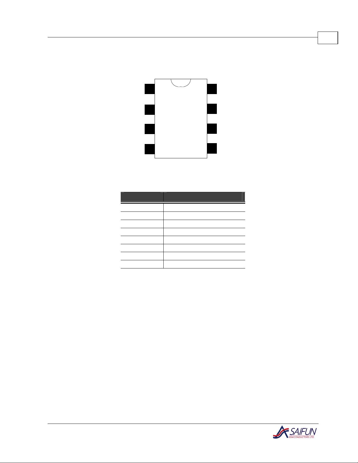
Connection Diagrams
4
CSb
SO
1
2
8
7
V
CC
HOLD
SA25C512
WPb
GND
Figure 1. SOIC 8 – Narrow/PDIP Package (Top View)
Pin Name Function
CSb Chip Select
SCK Serial Data Clock
SO Serial Data Output
GND Ground
VCC Power Supply
WPb Write Protect
HOLDb Suspend Serial Input
3
4
Table 1. Pin Names
SI Serial Data Input
6
5
SCK
SI
Page 5
SA25C512 Data Sheet
SAIFUN
Ordering Information
5
XYYELXXC25SA Letter
Blank
X
Package
Temp. Range
Voltage Operating Range
Density
Interface
Figure 2: SA25C512 Ordering Information
N
MN
Blank
E
L
H
512
C
25
SA
Description
Tube
Tape and Reel
8-pin DIP
8-pin SOIC (SO8, 150 mil width)
o
C
0 to 70
-40 to +85
2.7 V to 3.6 V
4.5 V to 5.5 V
512 Kb with Write Protect
CMOS Technology
SPI-2 Wires
Saifun Non-Volatile
Memory
o
C
Page 6

SA25C512 Data Sheet
SAIFUN
Product Specifications
Absolute Maximum Ratings
6
Ambient Storage Temperature
All input or output voltages with
respect to Ground
Lead Temperature
(Soldering, 10 seconds)
-65 °C to +150 °C
4.5 V to -0.3 V (L)
6.5 V to -0.3 V (H)
+235 °C
Latch Up Specifications
Latch Up
100 mA on all pins, +125°C
ESD Specifications
Human Body Model Per MIL-STD 883 Method 3015.7
Voltage Levels
Machine Model Per JEDEC standard JESD22-A115
Voltage levels
500 V to 5 KV, in increments of 500 V;
proceed to 8000 V or until failure
50 V to 300 V, in increments of 50 V;
proceed to 500 V or until failure
Operating Conditions
Ambient Operating Temperature:
SA25C512
SA25C512E
Positive Power Supply:
SA25C512L
SA25C512H
0 °C to +70 °C
-40 °C to +85 °C
2.7 V to 3.6 V
4.5 V to 5.5 V
Page 7

SA25C512 Data Sheet
SAIFUN
DC Characteristics
Applicable over recommended operating range from:
7
• T
• T
= -40 ºC to 85 ºC, VCC = 2.7-3.6 V/4.5-5.5 V
AI
= 0 ºC to 70 ºC, VCC = 2.7-3.6 V/4.5-5.5 V
AC
Table 2. DC Characteristics
Symbol Parameter Test Conditions
VCC
Supply Voltage
Limits
Min Typ* Max
Unit Comments
2.7 3 3.6 V L
4.5 5 5.5 V H
F
= 5 MHz, VCC = 5.0 V 4 8 mA L
SCK
F
= 2 MHz, VCC = 5.0 V 4 mA L
I
I
Active Power Supply
CC1
Current (Read)
Active Power Supply
CC2
Current (Write)
ISB Standby Current
IIL Input Leakage Current VIN = GND to VCC 1
IOL Output Leakage Current VIN = GND to VCC 1
SCK
F
= 5 MHz, VCC = 3.0 V 4 8 mA H
SCK
F
= 2 MHz, VCC = 3.0 V 4 mA H
SCK
Fwrite = 5 MHz,
Twrite = 10 ms
Fwrite = 2 MHz,
Twrite = 10 ms
Fwrite = 5 MHz,
Twrite = 10 ms
Fwrite = 2 MHz,
Twrite = 10 ms
VCC = 3.0 V,
CSb = V
V
CC
CSb = V
CC
= 5.0 V
CC
10 15 mA L
10 mA L
10 15 mA H
10 mA H
1
10
µA
µA
µA
µA
VIL Input Low Voltage -0.3 0.3 VCC V
V
+
VIH Input High Voltage 0.7 V
CC
CC
0.5
V
VOL Output Low Voltage IOL = 0.15 mA 0.2 V L
VOH Output High Voltage
IOH = -0.1 mA
V
CC
0.2
V L
VOL Output Low Voltage IOL = 3.0 mA 0.4 V H
VOH Output High Voltage
IOH = -1.6 mA
V
CC
0.8
V H
*Typical values are at TAI = 25 ºC and 3 V/5 V.
L
H
Page 8

SA25C512 Data Sheet
SAIFUN
AC Test Conditions
8
Input Levels
0.8Vcc
0.2Vcc
Input and Output
Timing Reference Levels
0.7Vcc
0.3Vcc
Figure 3. AC Measurements I/O Waveform
Table 3. AC Measurements
Symbol Parameter Min Max Unit
C
L
Load Capacitance 30 PF
Input Rise and Fall Times 5 NS
Input Pulse Voltage 0.2 VCC to 0.8 VCC V
Input and Output Timing
Reference Voltages
0.3 V
to 0.7 VCC
CC
V
Table 4. AC Characteristics
Symbol Parameter
F
SCK Clock Frequency 10 MHz
SCK
Min Typ Max
10 MHz
Unit
tWH SCK High Time 40 ns
tWL SCK Low Time 40 ns
tCS CSb High Time 50 ns
t
CSb Setup Time 50 ns
CSS
t
CSb HOLD Time 50 ns
CSH
tHD HOLD Time 25 ns
tCD HOLDB HOLD Time 25 ns
tV Output Valid 0 40 ns
tHO Output HOLD Time 0 ns
t
Data in HOLD Time 15 ns
HD:DAT
t
Data in Setup Time 12 ns
SU:DAT
tR Input Rise Time 2 ns
tF Input Fall Time 2 ns
tLZ HOLDb to Output Low Z 100 ns
tHZ HOLDb to Output High Z 100 ns
t
Output Disable Time 100 ns
DIS
tWC* 128-byte Page 8 ms
Endurance 100K Write cycles
* 128 bytes in the checkerboard programming formation; a maximum of 50% of the array is
programmed.
Page 9

SA25C512 Data Sheet
SAIFUN
9
Serial Interface Description
Master
The device that generates the SCK.
Slave
As the SCK pin is always an input, the
SA25C512 always operates as a slave.
Transmitter/Receiver
The SA25C512 has separate pins
designated for data transmission and
reception.
Serial Opcode
The first byte is received after the device is
selected. This byte contains the opcode
that defines the operation to be performed
(for more details, refer to Table 5,
page 10).
Invalid Opcode
If an invalid opcode is received, no data is
shifted into the SA25C512, and the serial
output pin remains in a high impedance
state until a CSb falling edge is detected
again, which reinitializes the serial
communication.
Chip Select (CSb)
HOLDb
The HOLDb pin is used in conjunction with
the CSb pin to select the SA25C512. When
the device is selected and a serial
sequence is underway, HOLDb can be
used to pause the serial communication
with the master device without resetting the
serial sequence. To pause, the HOLDb pin
must be brought low while the SCK pin is
low. To resume serial communication, the
HOLDb pin is brought high while the SCK
pin is low (SCK may still toggle during
HOLDb). Inputs to the SI pin are ignored
while the SO pin is in the high impedance
state.
Write Protect
The WPb pin enables write operations to
the Status register when held high. When
the WPb pin is brought low and the
WPBEN bit is 1, all write operations to the
status register are inhibited (for more
details, refer to Table 8, page 11). If WPb
goes low while CSb is still low, the write to
the status register is interrupted. If the
internal write cycle has already been
initiated, WPb going low has no effect on
any write operation to the status register.
The WPb pin function is blocked when the
WPBEN bit in the status register is 0,
which enables the user to install the
SA25F020 in a system with the WPb pin
tied to ground but still able to write to the
status register. All WPb pin functions are
enabled when the WPBEN bit is set to 1.
The SA25C512 is selected when the CSb
pin is low. When the device is not selected,
data is not accepted via the SI pin, and the
SO pin remains in a high impedance state.
Page 10

SA25C512 Data Sheet
SAIFUN
10
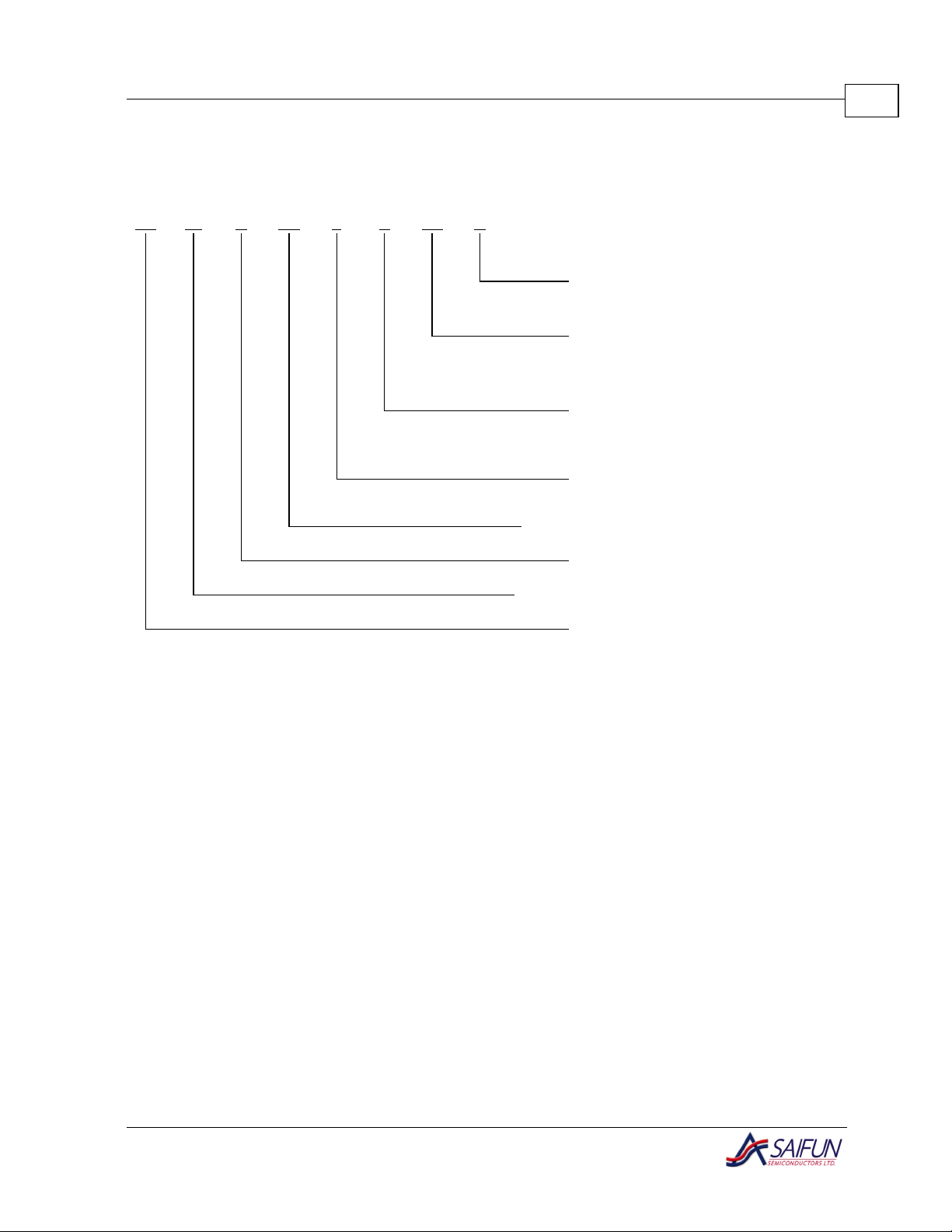
Functional Description
Figure 4 presents a schematic diagram of
the SPI serial interface.
MASTER:
MICROCONTROLL ER
DATA OUT
DATA IN
SERIAL CLOCK
SSO
SS1
SS2
SS3
SLAVE:
SA25C512
SI
SO
SCK
CS
SI
SO
SCK
CS
SI
SO
SCK
CS
Table 5. Instruction Set
Instruction
Name
Instruction
Format
Operation
WREN 0000X110 Set Write Enable Latch
WRDI 0000X100
Reset Write Enable
Latch
RDSR 0000X101 Read Status Register
WRSR 0000X001 Write Status Register
READ 0000X011
WRITE 0000X010
Read Data from
Memory Array
Write Data to Memory
Array
In addition to the instruction register, the
device also contains an 8-bit status register
that can be accessed by RDSR and WRSR
instructions. The byte defines the Block
Write Protection (BP1 and BP0) levels,
Write Enable (WEN) status, Busy/Rdy
(/RDY) status and Hardware Write Protect
(WPBEN) status of the device. Table 6
illustrates the format of the status register.
SI
SO
SCK
CS
Figure 4. SPI Serial Interface
The SA25C512's SPI consists of an 8-bit
instruction register that decodes a specific
instruction to be executed. Six different
instructions (called opcodes) are
incorporated in the device for various
operations. Table 5 lists the instructions set
and the format for proper operation. All
opcodes, array addresses and data are
transferred in an MSB-first-LSB-last
fashion. Detailed information about each of
these opcodes is provided under individual
instruction descriptions in the sections that
follow.
Table 6. Status Register Format
Bit 7 Bit 6 Bit 5 Bit 4 Bit 3 Bit 2 Bit1 Bit 0
WPBEN X X X BP1 BP0 WEN /RDY
Write Enable (WREN)
The device powers up in the Write Disable
state when V
is applied. All programming
CC
instructions must be preceded by a WREN
instruction.
Write Disable (WRDI)
To protect the device against inadvertent
writes, the WRDI instruction disables all
programming modes. The WRDI
instruction is independent of the WP pin's
status.
Page 11

SA25C512 Data Sheet
SAIFUN
11
Read Status Register (RDSR)
The RDSR instruction provides read
access to the status register. The
BUSY/RDY and WREN statuses of the
device can also be determined by this
instruction. In addition, the Block Write
Protection bits indicate the extent of
protection employed. In order to determine
the status of the device, the value of the
/RDY bit can be continuously polled before
sending any write instruction.
Write Status Register (WRSR)
The WRSR instruction enables the user to
select one of four levels of protection. The
SA25C512 is divided into four array
segments. The top quarter, top half or all of
the memory segments can be protected
(for more details, refer to Table 7). The
data within a selected segment is therefore
read-only.
Table 7. Block Write Protect Bits
Status Register Bits
Level
BP1 BP0
0 0 0 None
1/4 0 1 C000 - FFFF
1/2 1 0 8000 - FFFF
All 1 1 0000 - FFFF
The WRSR instruction (as shown in
Table 8) also allows the user to enable or
disable the WPb pin via the WPBEN bit.
Hardware write protection is enabled when
the WPb pin is low and the WPBEN bit is
1, and disabled when either the WP pin is
high or the WPBEN bit is 0. When the
device is hardware write protected, writes
to the status register are disabled.
Array Addresses
Protected
NOTE:
When the WPBEN bit is hardware write
protected, it cannot be changed back
to 0 as long as the WPb pin is held low.
Table 8. WPBEN Operation
WPb WPBEN WEN
X 0 0 Protected Protected Protected
X 0 1 Protected Writable Writable
Low 1 0 Protected Protected Protected
Low 1 1 Protected Writable Protected
High X 0 Protected Protected Protected
High X 1 Protected Writable Writable
Protected
Blocks
Un-
protected
Blocks
Status
Register
Read Sequence (READ)
Reading the SA25C512 via the SO pin
requires the following sequence (for more
details, see Table 9, page 12):
1. After the CSb line is pulled low to select
the device, the READ opcode is
transmitted via the SI line, followed by
the byte address to be read. Upon
completion, any data on the SI line is
ignored.
2. The data (D7-D0) at the specified
address is then shifted out onto the SO
line.
If only one byte is to be read, the CSb line
should be driven high after the data comes
out. The READ sequence can be
continued, as the byte address is
automatically incremented and data
continues to shift out. When the highest
address is reached, the address counter
rolls over to the lowest address, enabling
the entire memory to be read in one
continuous READ cycle.
Page 12

SA25C512 Data Sheet
SAIFUN
12
Table 9. Read Status Register Definition
Bit Definition
Bit 0 = 0 (/RDY) indicates that the
Bit 0 (/RDY)
Bit 1 (WEN)
Bit 2 (BP0) Block Write Protect Bit 0
Bit 3 (BP1) Block Write Protect Bit 1
Bit 7
(WPBEN)
Bits 4-6 are 0s when the device is not in an internal
write cycle; bits 0-7 are 1s during an internal write
cycle.
device is READY.
Bit 0 = 1 indicates that a write cycle
is in progress.
Bit 1 = 0 indicates that the device is
not write enabled.
Bit 1 = 1 indicates that the device is
write enabled.
Write Protect Mode Enable Bit
Write Sequence (WRITE)
Two separate instructions must be
executed in order to write to the
SA25C512. The device must first be write
enabled via the WREN instruction, and
then a WRITE instruction may be
executed. The address of the memory
locations to be written must be outside the
protected address field location selected by
the Block Write Protection level. During an
internal write cycle, all commands are
ignored except the RDSR instruction.
A WRITE instruction requires the following
sequence:
1. After the CSb line is pulled low to select
the device, the WRITE opcode is
transmitted via the SI line, followed by
the byte address and the data (D7-D0)
to be written.
2. Programming starts after the CSb pin is
brought high. The CSb pin's low-to-high
transition must occur during the SCK
low time, immediately after clock in the
D0 (LSB) data bit.
The SA25C512 is capable of up to a
128-byte (from 1 to 128 bytes) PAGE write
operation. After each byte is received, the
eight low-order address bits are internally
incremented by one. If more than 128
bytes of data are transmitted, the address
counter rolls over and the previously
written data is overwritten. The SA25C512
is automatically returned to the write
disable state at the completion of a write
cycle.
NOTE:
If the device is not write enabled, the
device ignores the WRITE instruction
and returns to the standby state when
CSb is brought high. A new CSb falling
edge is required to re-initiate the serial
communication.
Page 13

SA25C512 Data Sheet
SAIFUN
Timing Diagrams
All timing diagrams are based on SPI protocol modes 0 and 1.
t
CS
t
DIS
HI-ZHI-Z
CS
SCK
SO
v
IH
v
IL
t
CSS
v
IH
v
IL
t
v
IH
SI
v
IL
v
OH
v
OL
SU
VALID IN
t
WH
t
H
t
WL
t
V
t
HO
t
CSH
13
CS
SCK(0,0)
SCK(1,1)
SI
Figure 5. SPI Mode 0 (0,0) Timing
Figure 6. SPI Mode 0 (0,0) and 3 (1,1) Timing
Page 14

SA25C512 Data Sheet
SAIFUN
CS
SCK
HOLD
t
CD
t
HD
t
HD
t
HZ
t
CD
14
CS
SCK
SO
CS
SCK
SO
t
LZ
Figure 7. HOLDb Timing
1 3210987654023222120
Instruction 16-Bit Address
1314
SI
High Impedance
15
132 0
76543210
MSB
2827262524 313029
DATA OUT 1 DATA OUT 2
7
MSB
Figure 8. Read Timing
1 3210987654023222120
2827262524 313029
Instruction 16-Bit Address
SI
MSB MSB
1314
15 132 0 576 4 132 0
Data Byte 1
Figure 9. Write Timing
Page 15

SA25C512 Data Sheet
SAIFUN
CSb
1 32109876540 14131211 15
SCK
Instruction Status Register In
15
SI
SO
CS
SCK
SI
SO
13210987654014131211
Instruction
High Impedance
MSB
High Impedance
Figure 10. Write Status Register Timing
7 6 5 4 3 2 1 0
MSB
132 07654
Data Out
Figure 11. Read Status Register Timing
Page 16

SA25C512 Data Sheet
SAIFUN
Physical Dimensions
All measurements are in inches (millimeters), unless otherwise specified.
16
Figure 12. 8-pin SOIC Package
Page 17

SA25C512 Data Sheet
SAIFUN
17
Figure 13. 8-pin Molded Small Outline Package (MN), 0.150” Wide Body, JEDEC SOIC
Page 18

SA25C512 Data Sheet
SAIFUN
18
Figure 14. Molded Dual-in-line Package (N) Package Number N08E
Page 19

SA25C512 Data Sheet
SAIFUN
Saifun Semiconductors Ltd. Headquarters
ELROD Building
45 Hamelacha St.
Sappir Industrial Park
Netanya 42505
Israel
Tel.: +972-9-892-8444
Fax: +972-9-892-8445
Email: tech_support@saifun.com
http://www.saifun.com
Revision History
Rev Date Description of Change Amendment
1.0 1-Sep-02 Initial Release 0
19
1.1 27-Jan-03 Document promoted from “Advanced
Information” to “Data Sheet”, ESD scheme
modification, Figure 8 modified
1
Prepared by Approved by Approved by Signature
Golan M. Shalhov
Product Line Manager
© Saifun Semiconductors Ltd. 2003
Saifun reserves the right, without notice, to change any of the products described in this guide, in order to improve functionality,
reliability or design. Saifun assumes no liability arising from the application or use of any product described in this guide; and
under its patent rights, gives no authorization for the use of this product or associated products. The Buyer will not hold Saifun
responsible for direct or indirect damages and expenses, as well as any claim of injury or death, associated with the
unauthorized use, including claims of manufacture or design negligence.
Other company and brand products and service names are trademarks or registered trademarks of their respective holders.
Shai Eisen
Design Project Manager
Doron Vertesh
Director EEPROM SBU
27-Jan-03
Date
Life Support Policy
Saifun's products are not authorized for use as critical components in life support devices or systems without the express written
approval of the President of Saifun Semiconductors Ltd. As used herein:
1. Life support devices or systems are devices or
systems which, (a) are intended for surgical implant
into the body, or (b) support or sustain life, and whose
failure to perform, when properly used in accordance
with instructions for use provided in the labeling, can
be reasonably expected to result in a significant injury
to the user.
2. A critical component is any component of a life
support device or system whose failure to perform can
be reasonably expected to cause the failure of the life
support device or
effectiveness.
system, or to affect its safety or
 Loading...