

Page 1

SA2531 A/B/C/E/G/U
sames
VERSATILE SINGLE CHIP TELEPHONE
WITH 14 NUMBER REPERTORY DIALLER
FEATURES
■ Speech circuit, LD/MF Repertory Dialler
and Tone Ringer on one 28 pin CMOS
chip
■ Net 4 compatible
■ Soft clip to avoid harsh distortion
■ Line Loss Compensation selectable by
pin option
■ Power down mode
■ Versatile applications for different PTT
demands
■ 31 digit last number redial
■ Sliding Cursor protocol with comparison
■ 2 Flash keys, 100 ms and 280 ms (option
600 ms)
■ Ring frequency discrimination
SA2531 A/B/C/D/E/F/G/J/U
■ Operating range from 13 to 100 mA
(down to 5 mA with reduced performance)
■ Volume control of receive signalExcept
"D")
■ Low noise (max. -72dBmp)
■ Real or Complex impedance on chip pro-
grammable
■ LD/MF switchable dialling
■ 14 memories, 4 direct/10 indirect or 10
direct
■ Pause key for 2, 3 or 6 sec Auto Pause or
Wait function
■ On chip MF filter (CEPT CS 203 compat-
ible)
■ 3-tone melody generator
GENERAL DESCRIPTION
The SA2531 is a CMOS integrated circuit that contains all the functions needed to form a high
performance electronic telephone.
The device incorporates LD/MF repertory dialling, melody generation, ring frequency
discrimination and a high quality speech circuit.
A RAM is on chip for a 31 digit last number redial and 14 memories each containing up to 21
digits. The sliding cursor procedure makes Last Number Redial easy behind a PABX.
The SA2531 (exept the SA2531D) incorporates a volume control for the earpiece. The receive
volume can be controlled by the VOL key (+4dB) or by the +/- keys (+6dB/-4dB in 5 steps).
The versatility of the circuit is provided by on chip programmability and a few external
components. This allows easy adaption to different PTT requirements without changing the
PCB of the telephone.
sames
M82-2013 PDS039-SA2531-001 Rev.D 15-05-97
1/24
Page 2
SA2531 A/B/C/E/G/U
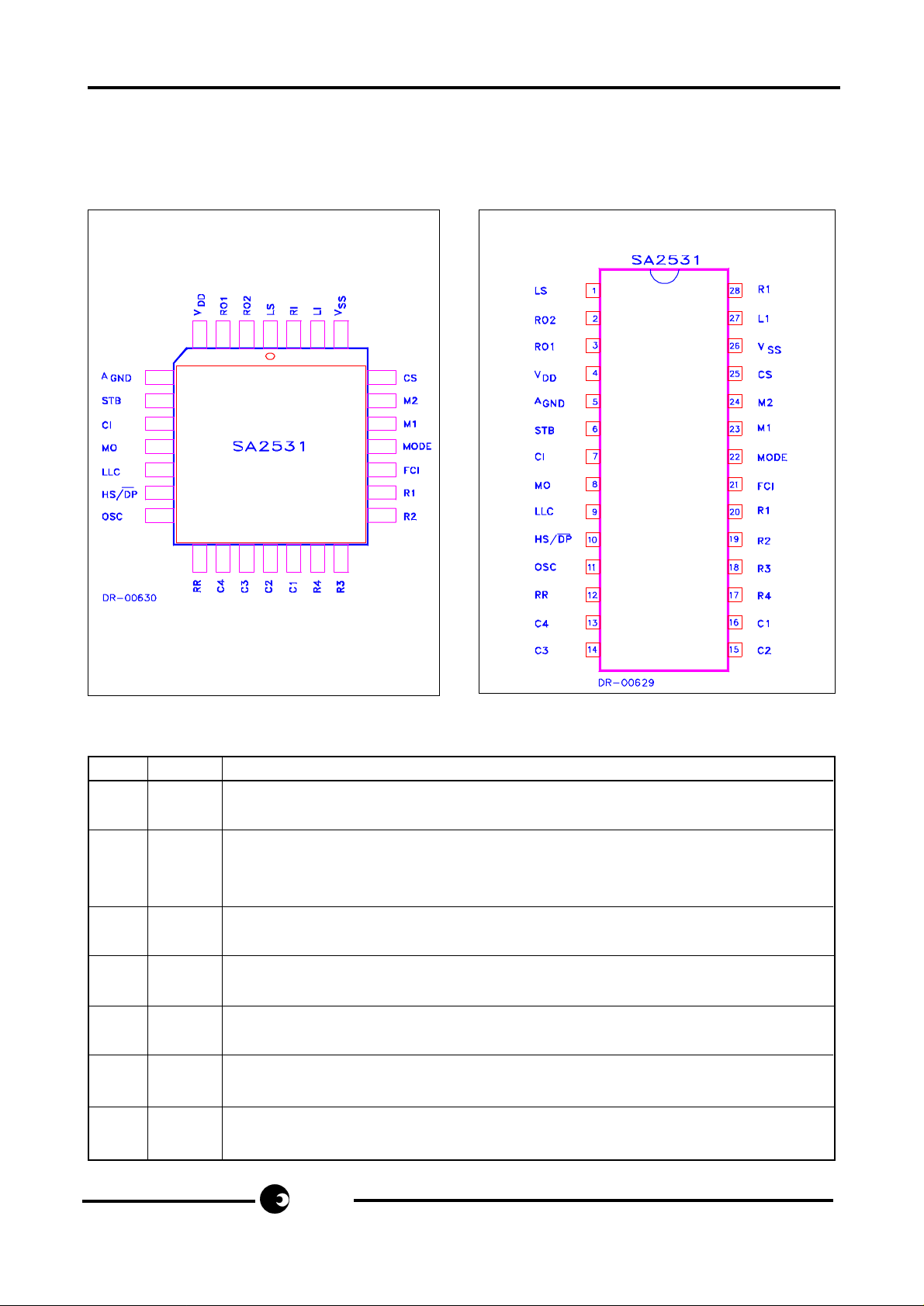
PACKAGE
Available in 28 pin DIP and PLCC
PIN CONFIGURATIONS
28 Pin PLCC
28 Pin DIP
PIN DESCRIPTION
Pin# Symbol Function
23 M1 Microphone Inputs
24 M2 Differential inputs for the microphone (electret).
3 RO1 Receiver Outputs
2 RO2 These are the outputs for driving a dynamic earpiece with an impedance
of 150 to 300Ω
5A
GND
Analogue Ground
This is the analog ground for the amplifiers.
28 RI Receive Input
This is the input for the receive signal.
6 STB Side Tone Balance Input
This is the input for side tone cancellation.
1LS Line Current Sense Input
This is the input for sensing the line current.
27 LI Line Input
This input is used for power extraction and line current sensing.
2/24
sames
Page 3

Pin# Symbol Function
25 CS Current Shunt Control Output
This N-channel open drain output controls the external high power shunt
transistor for the modulation of the line voltage and for shorting the line
during make period of pulse dialling.
4V
DD
Positive Voltage Supply
This is the supply pin for the circuit.
26 V
SS
Negative Power Supply
8MOMelody Output
Pulse Density Modulated output of the melody generator for tone ringer. At
high impedance when not active.
21 FCI Frequency Comparator Input
This is a Schmitt trigger input for ring frequency discrimination. Disabled
during off-hook.
10 HS/DP Hook Switch Input and Dial Pulse Output
This is an I/O that is pulled high by the hook switch when off- hook. An open
drain pulls it low during break periods of pulse dialling and flash.
11 OSC Oscillator Input
Oscillator pin for Xtal or ceramic resonator (3.58 MHz). Recommended part
is the Murata CSA3.5MG312AM.
9 LLC Line Loss Compensation
Select pin for the loss compensation.
OPEN = None V
= 45-75mA VDD = 20-50mA
DD
12 RR Repetition Rate
Select pin for repetition rate of melody for the Tone rinser.
22 MODE Signalling Mode Select Input
Mode pin Function
High LD mode, 10pps, M:B = 33:66 (J:20pps)
Open MFonly
Low LD mode, 10pps, M:B = 40:60 (J:20pps, M:B = 33:66)
SA2531 A/B/C/E/G/U
20 R1 Keyboard Rows
19 R2
18 R3
17 R4
16 C1 Keyboard Columns
15 C2
14 C3
13 C4
7CI Complex Impedance Input
Input pin for the capacitor in the complex impedance
sames
3/24
Page 4

SA2531 A/B/C/E/G/U
FUNCTIONAL DESCRIPTION
Power On Reset
The on chip power on reset circuit monitors the supply voltage (VDD). When VDD rises above
approx. 1.2V, a power on reset occurs to assure correct start-up and the RAM is cleared.
DC Conditions
The normal operating range is from 13mA to 100 mA. Operating range with reduced
performance is from 5mA to 13mA. In the operating range all functions are operational.
At line currents below 13mA the SA2531 provided an additional scope below 4.5V to allow
parallel operation. (See Figure 12).
The dc characteristic (excluding diode bridge and Pulsing transistors) is determined by the
voltage at LI and the resistor R1 as follows:
VLS = VLI + I
Line
.R1
The voltage at LI is 4.5V.
During pulse dialling the speech circuit and other parts of the device not required are in a
power down mode to save current. The CS pin is pulled to V
in order to turn the external
SS
shunt transistor on to keep a low voltage drop at the LS pin during make periods.
AC Impedance
The Characteristic or Output impedance of the SA2531 is set within the IC and adjusted by
Mask Options. Available options are for 600Ω and 1000Ω. When the 1000Ω option is selected
then a capacitor may be added to the circuit at pin CI to add a reactive element and make the
output impedance complex.
Oscillator
All the Timing Functions of the SA2531 are based on a Clock Frequency of 3.58MHz. A crystal
or ceramic resonator of this frequency should be connected to the OSC pin. In practise minor
deviations from the nominal frequency may occur due to the characteristics of the frequency
reference device used and so it is recommended that care is taken in the selection of
components.
Typically a small value capacitor ( ≤47pF) should be connected in parallel with the Frequency
Reference to ensure start-up and/or operation at the nominal frequency.
Speech Circuit
The speech circuit consists of a transmit and a receive path born with soft clip, mute, line loss
compensation and side tone cancellation.
Transmit
The gain of the transmit from M1/M2 to LS is 35dB for 600Ω versions and 37dB for 1000Ω
versions (see test circuit figure 5). The microphone input is differential with an input
impedance of 25 kΩ.
The soft clip circuit limits the output voltage at LI to 2.0V
(see figures 8 & 9). The attack
PEAK
time is 30µs/6dB and the decay time is 20 ms/6 dB. When mute is active, during dialling
4/24
sames
Page 5
SA2531 A/B/C/E/G/U
or after pressing the MUTE key, the gain is reduced by > 60 dB.
Receive
The receive input is the differential signal of RI and STB. The gain of the receive path
is 2 dB (test circuit figure 5) with differential outputs, RO1/RO2 (0dB on 1000Ω versions).
When mute is active during dialling the gain is reduced by > 60dB. During DTMF dialling
a MF comfort tone is applied to the receiver. The comfort tone is the DTMF signal with
a level that is -30dB relative to the line signal.
The receive gain can be adjusted under user control by using the volume control keys (not
on SA2531D). The VOL key gives a 4dB increase or returns the gain to normal in a Toggle
Function. Alternatively the + and - keys may be used. The + key increases the gain to
a maximum of +6dB while the - key reduces the gain to a minimum of -4dB. Each press
of the keys changes the gain by approximately 2dB.
The gain is reset by the next on-hook.
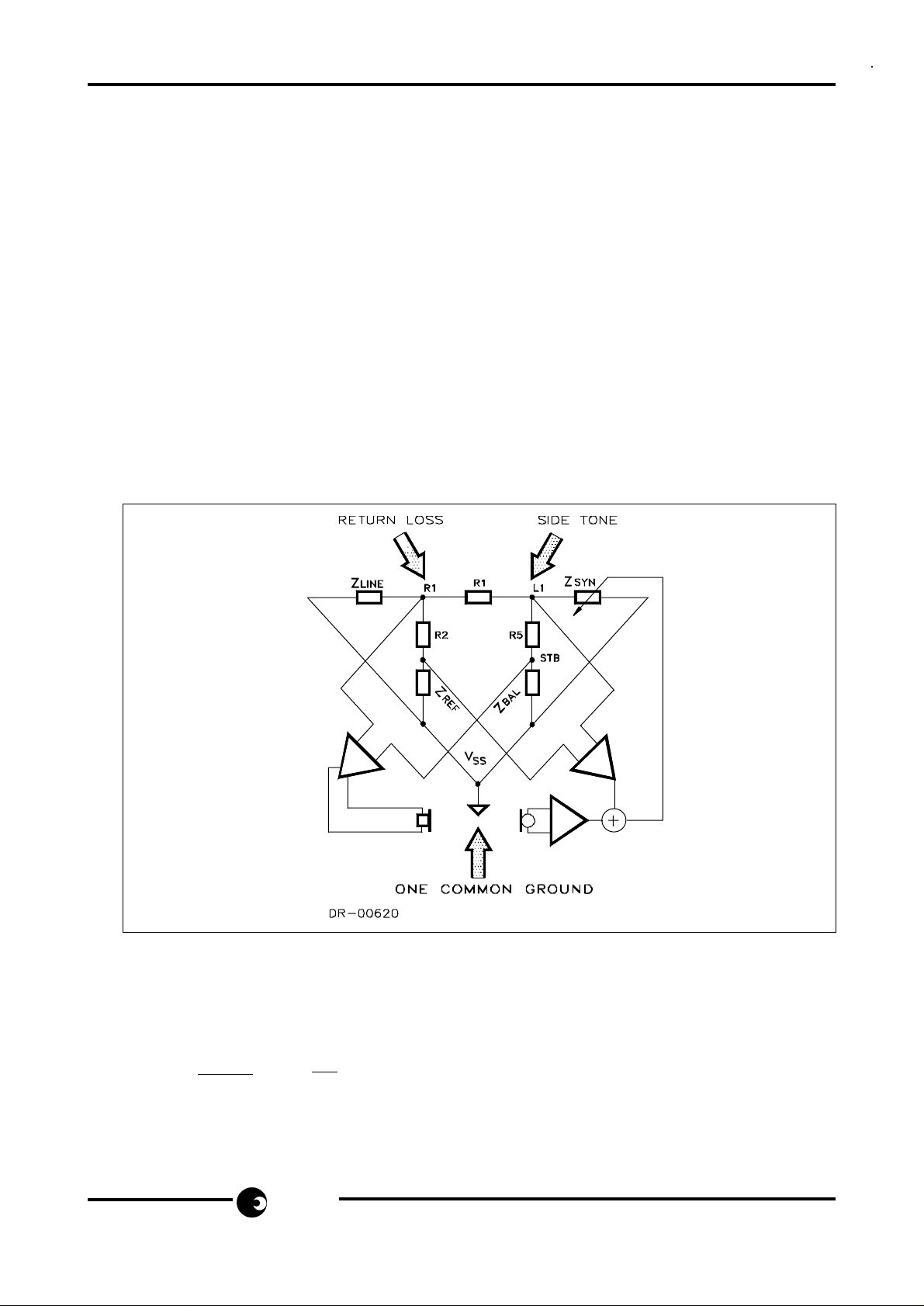
Side Tone
Side Tone is controlled along with Return Loss by a Double Balance Bridge as shown in
Fig. 1.
Figure 1
Double balance bridge (return loss and side tone) with one common ground
A good side tone cancellation is achieved by using the following equation:
ZBAL = R5
ZLINE R1
sames
5/24
Page 6

SA2531 A/B/C/E/G/U
The side tone cancellation signal is applied to the STB input.
Line Loss Compensation
When Line Loss Compensation is active the gain of the Transmit and Receive amplifiers
are changed by 6dB in accordance with the DC conditions as measured at Pins LI and
LS. When the LLC Pin is Low this adjustment in gain occurs over the range I
50 mA. When LLC is High the range is 45 to 75mA. Note that these figures apply for R1
= R30Ω.
When the LLC Pin is open the amplifier gains remain fixed regardless of the Line Current
(see figures 6 & 7).
Dialling Functions
Valid Keys
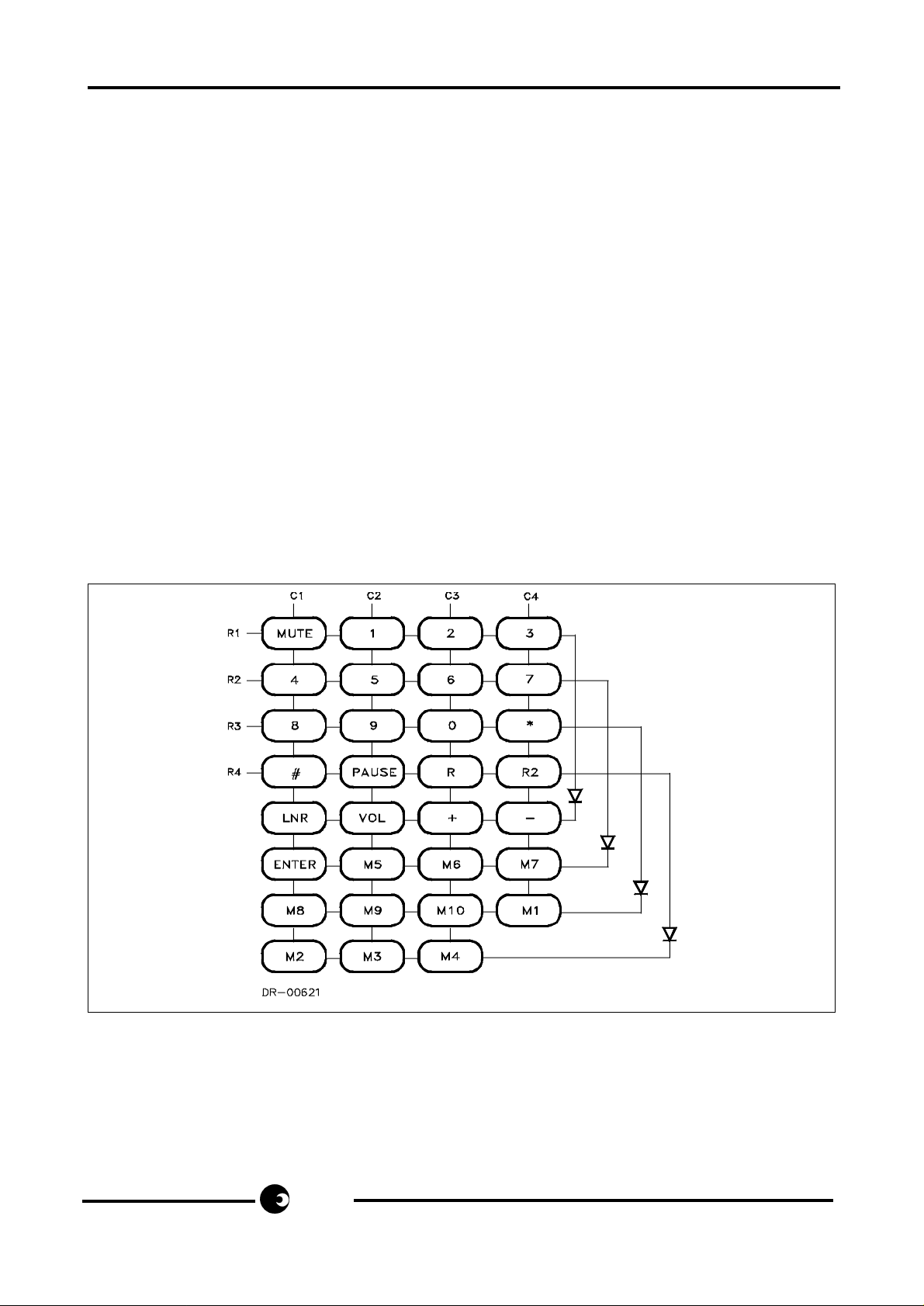
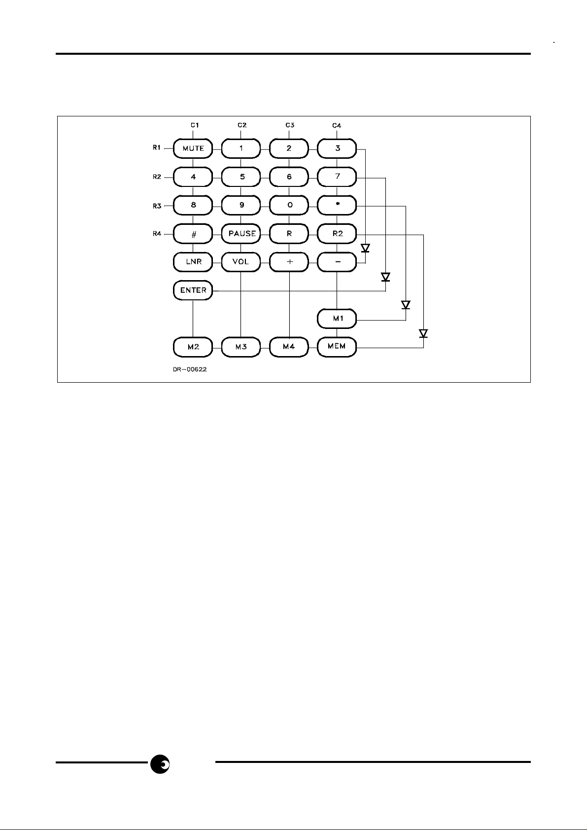
The keypad of the SA2531 comprises a maximum of 32 keys some of which are provided
to cater for options (such as the two Recall/Flash periods). A Bi-polar scan technique is
used so that the 32 keys are scanned in a 4 x 8 matrix using only 8 pins. Two explanatory
keypad arrangements are illustrated in Figures 2 & 3.
= 20 to
LINE
A valid key is detected when one and only one contact closure is detected between a Row
and Column Pin. Key contacts are debounced to avoid incorrect detection.
It is also possible to drive the keypad inputs with a micro controller.
Dial Mode Selection
The default mode (LD or MF) can be selected by the Mode pin. When default LD mode
is selected, a temporary change to MF can be invoked by pressing the * key. The circuit
will revert to LD by pressing the R (or R2) key or by next on-hook.
When MF mode is selected by the mode pin, the circuit can not be changed temporary
to LD but will remain in MF.
Last Number Redial
LNR is a facility that allows resignalling of the last manually dialled number without keying
in all the digits again. The LNR is repeatable.
The current contents of the RAM are overwritten by new entries.
A manually entered number is automatically stored in the LNR RAM. The capacity of the
RAM is 31 digits. If a number greater than 31 digits is entered, the LNR facility will be
inhibited (Until new entries < 32 digits) and further entries will be buffered in a First In First
Out Memory (FIFO).
6/24
sames
Page 7

SA2531 A/B/C/E/G/U
Post dialled digits, i.e. digits manually entered after LNR has been invoked, are not stored
in RAM but buffered in FIFO.
Pauses can be inserted by pressing the PAUSE key. (Further details of the Pause
Function are included in the Memory Keys section.)
Recall Function
A Recall (R key or R2 key) activation will invoke a Flash (Timed Loop Break).
If Recall is the first entry in a digit string, it will be stored in LNR RAM when digit(s) are
entered after the Recall.
If the recall key is depressed after a digit string has been entered or dialled out, the recall
will not be stored but buffered in the FIFO together with subsequently entered digits.
If pressing the recall key is not followed by digit entries, the LNR RAM remains intact.
After a recall a pause of 27ums or 3 seconds will automatically be executed.
On versions C/C/E/G a recall cannot be executed in LD mode.
Memory Keys
The keys M1 to M10 are direct memory access keys and the MEM key is used for indirect
or abbreviated dialling.
In the on chip RAM, 14 numbers can be stored. Each number can contain up to 21 digits
(including pauses).
During programming multiple pauses can be inserted by pressing the PAUSE key or the
LNR key. Each pause is 3 seconds (optionally 6 or 2 seconds) when inserted within the
first 5 digits otherwise a wait function that will halt dialling until the PAUSE key or the LNR
key is depressed.
Memory dialling is cascadable. However, the content of one memory must be dialled out
before a new one can be invoked.
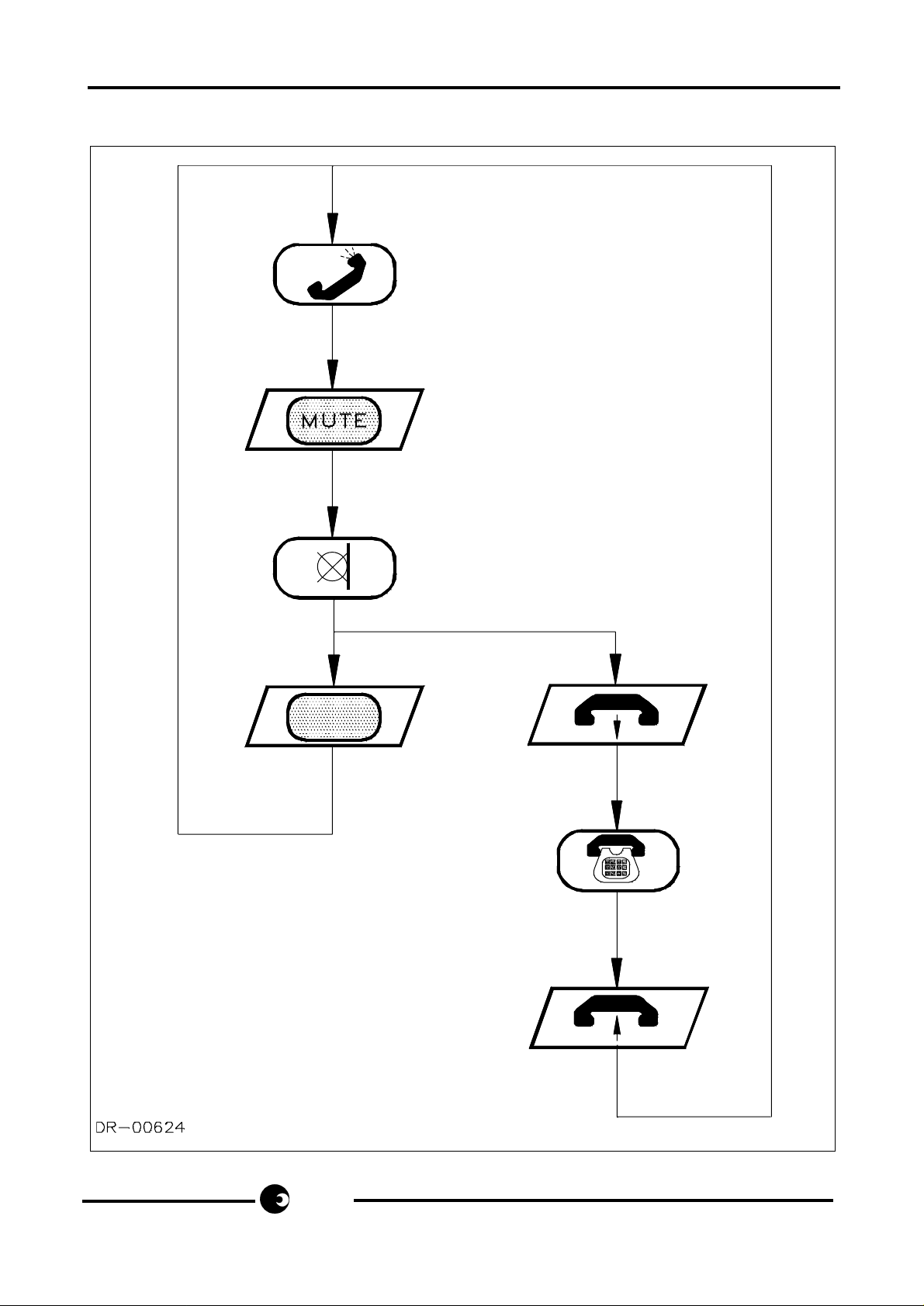
Mute Function
The MUTE key is enabled in speech mode only. Depressing the MUTE key mutes the
microphone amplifier. Repressing the MUTE key deactivates the mute (toggle function).
Any key entry overwrites a mute activated by the MUTE key and mute will be deactivated.
When privacy mute is activated a reminder tone is applied to the earpiece.
Sliding Cursor Procedure
To accommodate easy and uncomplicated redialling (LNR) behind a PABX, a sliding
cursor protocol is implemented. If new entries match the previous RAM contents, pressing
the LNR key will dial out the remaining digits.
If there is an error in matching, the LNR will be inhibited until next on-hook, and the RAM
will contain the new number.
sames
7/24
Page 8
SA2531 A/B/C/E/G/U
Tone Generator
The tone generator incorporates the DTMF tones and 3 basic frequencies for the tone
ringer.
DTMF Tones
The DTMF Tone Generator creates 12 Tones in compliance with CCITT Recommendation Q23. Signal levels are altered by Mask Option. High group frequencies have a level
2.6dB higher than those of the Low Group.
Details of the DTMF Tones are:
Low group
Digit 1-2-3 697Hz (Error = -.074%)
Digit 4-5-6 770Hz (Error = -.679%
Digit 7-8-9 852Hz (Error = -.621%)
Digit *-0-# 941Hz (Error = +.139%)
High group
Digit 1-4-7-* 1209Hz (Error = +.533%)
KEYBORD ARRANGEMENT 1
10 Direct memories (either VOL or +/- keys)
8/24
Figure 2
sames
Page 9
SA2531 A/B/C/E/G/U
KEYBORD ARRANGEMENT 2
4 Direct and 10 Indirect memories
(either VOL or +/- keys)
Figure 3
Tone Ringer
The Tone Ringer of the SA2531 incorporates a Discriminator Circuit and adjustable Melody
Generator
Ring Frequency Discrimination
The Ring Frequency Discriminator assures that only signals with a frequency between
20Hz and 60Hz (option 13 Hz to 70 Hz) are regarded as valid ring signals.
When a valid ring signal is present for 73 ms continuously, the melody generator is
activated and remains active as long as the ring signal is present.
Once the melody generator has been started, the ring signal is continuously monitored
and the melody generator is instantly turned on or off according to the momentary
presence of a valid or unvalid ring signal respectively (until next POR of off-hook).
Melody Generator
When a Valid Ring Signal is detected the Melody generator is activated and creates a
ringing Signal comprising 3 frequencies F1 (800Hz), F2 (1067Hz) and F3 (1333Hz).
These frequencies are repeated in a sequence of 6 time slots constructed by the
frequencies
F1 F2 F3 F1 F2 F3
This seqeunce is repeated 1, 4, 7 or 10 times per second as indicated by the connection
of the RR Pin to one of the four rows of the keyboard.
sames
9/24
Page 10
SA2531 A/B/C/E/G/U
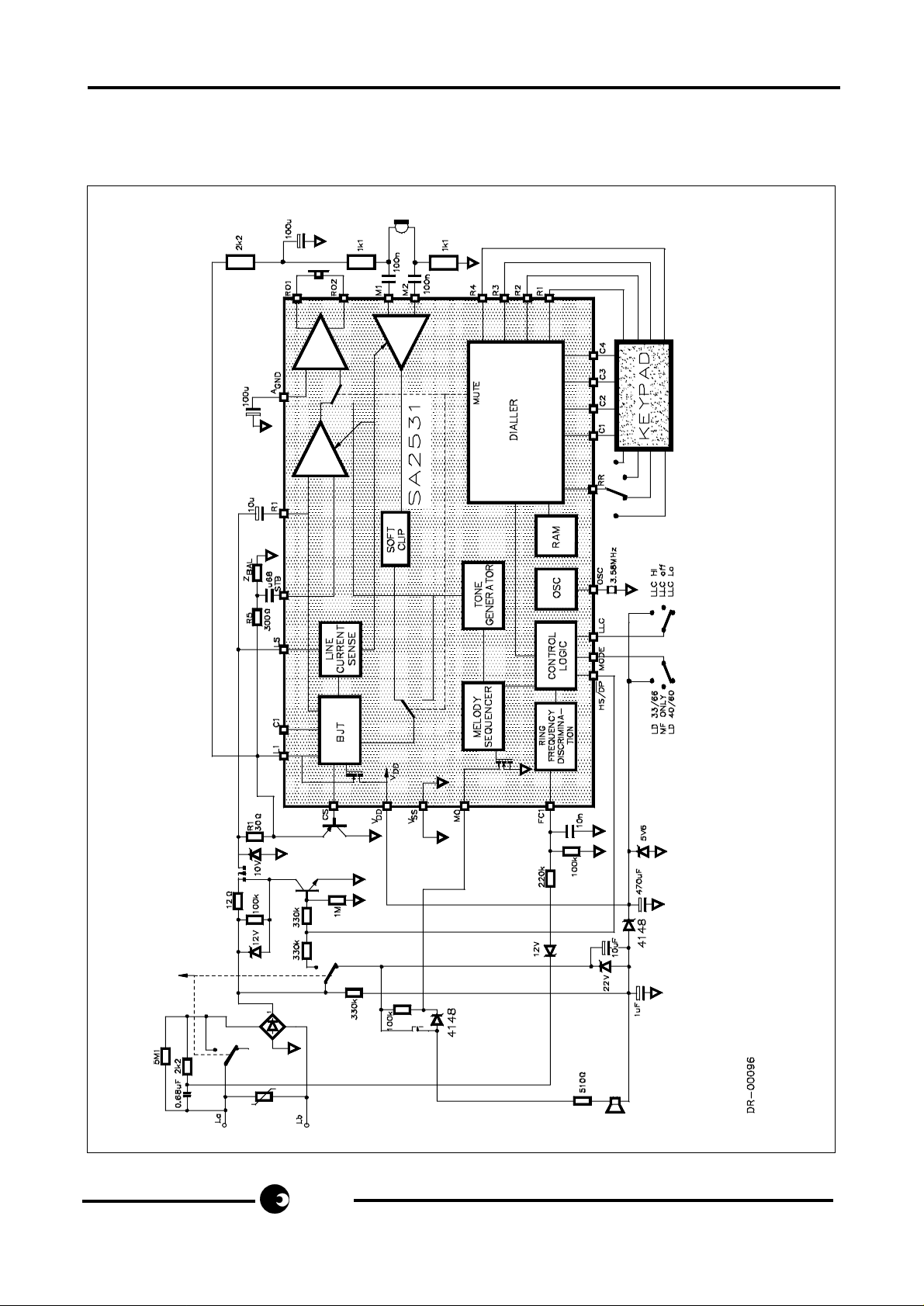
TYPICAL APPLICATION
Only the components necessary for presenting the complete functions of
the SA2531 are included.
10/24
sames
Page 11
SA2531 A/B/C/E/G/U
Digit 2-5-8-0 1336 Hz (Error = +.176%)
Digit 3-6-9-# 1477Hz (Error = -.141%)
Errors are calculated with reference to a base clock of 3.58MHz and at ambient
temperature of 24°C. They exclude tolerance errors in the base frequency.
OPERATING PROCEDURES
Procedure Principles
The procedures for utilizing the features of the SA2531 are optimized out of consideration for
the human factor in order to:
- meet the user’s expectations
- be easy to learn and relearn
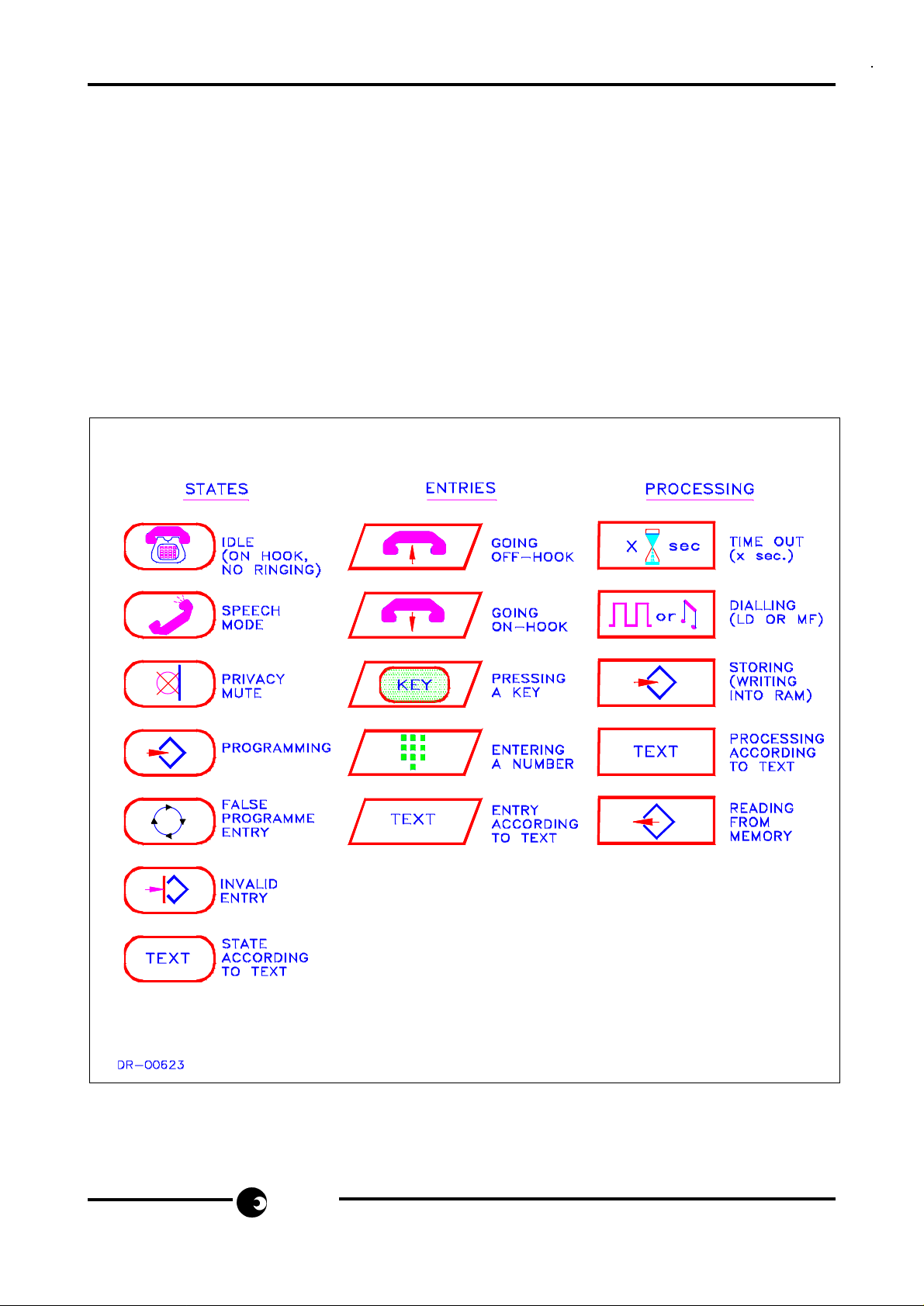
SYMBOLS
sames
11/24
Page 12
SA2531 A/B/C/E/G/U
Privacy Mute
12/24
sames
Page 13
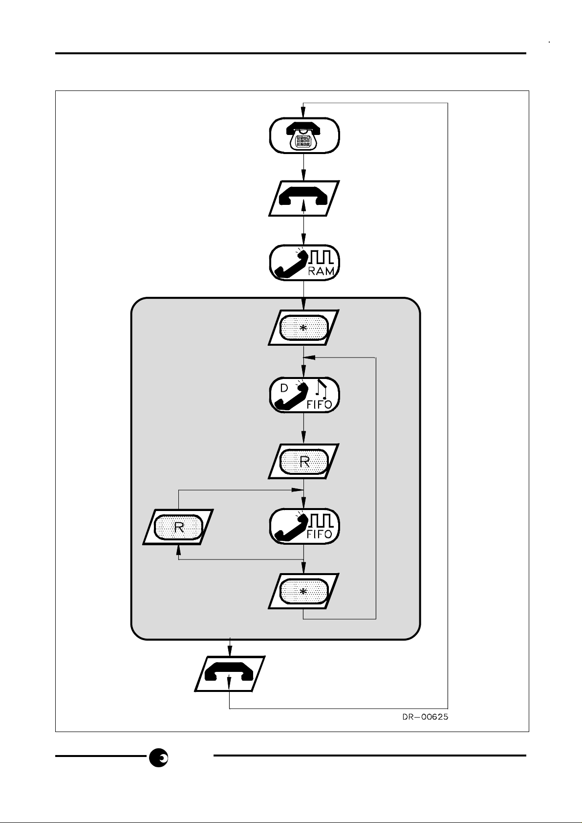
Temporary MF
SA2531 A/B/C/E/G/U
FIFO
Pressing any other
key does not
change the state.
EXIT FIFO
sames
13/24
Page 14
SA2531 A/B/C/E/G/U
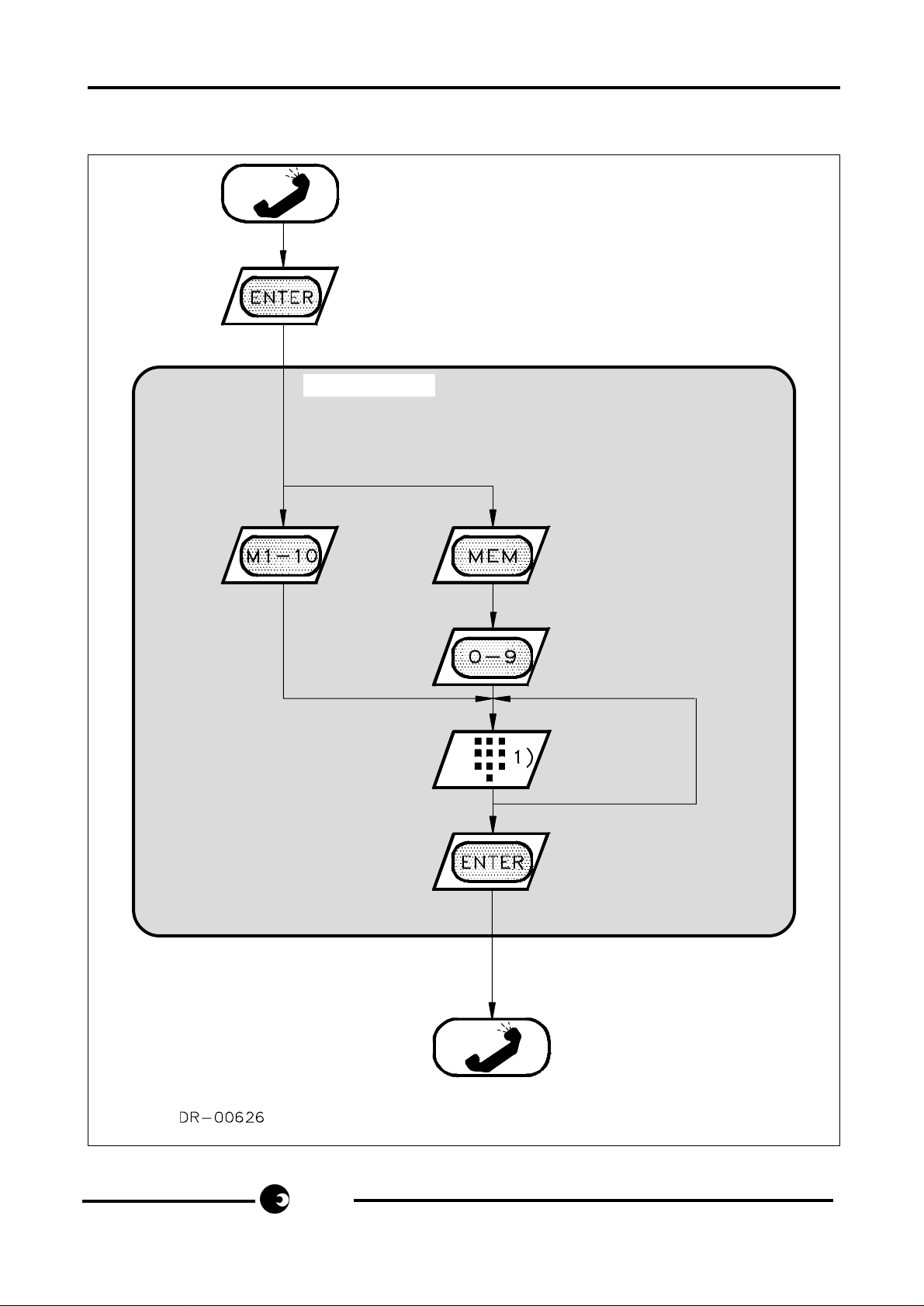
Storing Numbers
Key entries different to the procedure will be ignored.
Exit programme mode from each state with on-hook
or ENTER.
Programme State
1) Entries (0 - 9, *, #, PAUSE, R, R2) will be stored
immediately into the selected memory.
14/24
sames
Page 15
Automatic Dialling
SA2531 A/B/C/E/G/U
sames
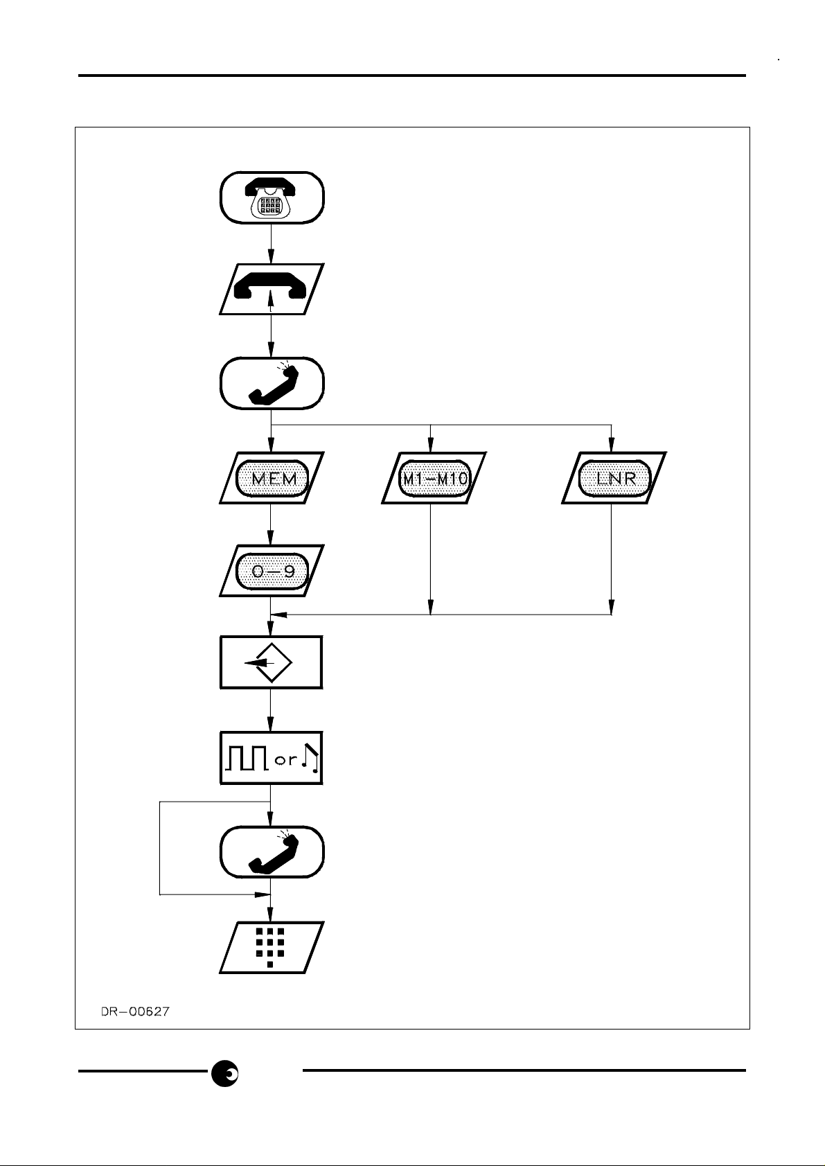
Postdailled digits are not stored
but buffered in FIFO
15/24
Page 16
SA2531 A/B/C/E/G/U
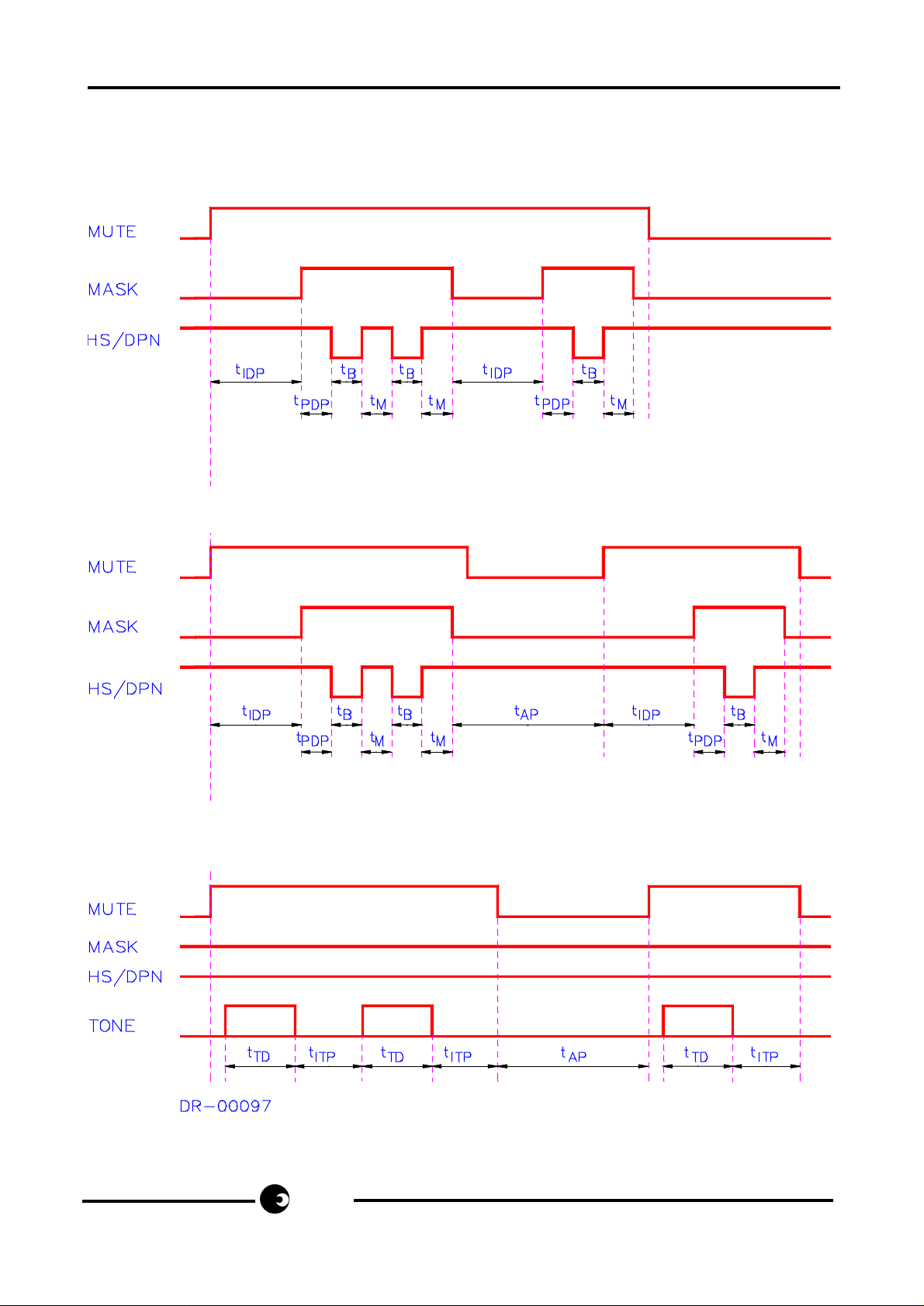
TIMING DIAGRAMS
LD Dialling
LD Dialling with Access Pause
MF Dialling
16/24
sames
Page 17
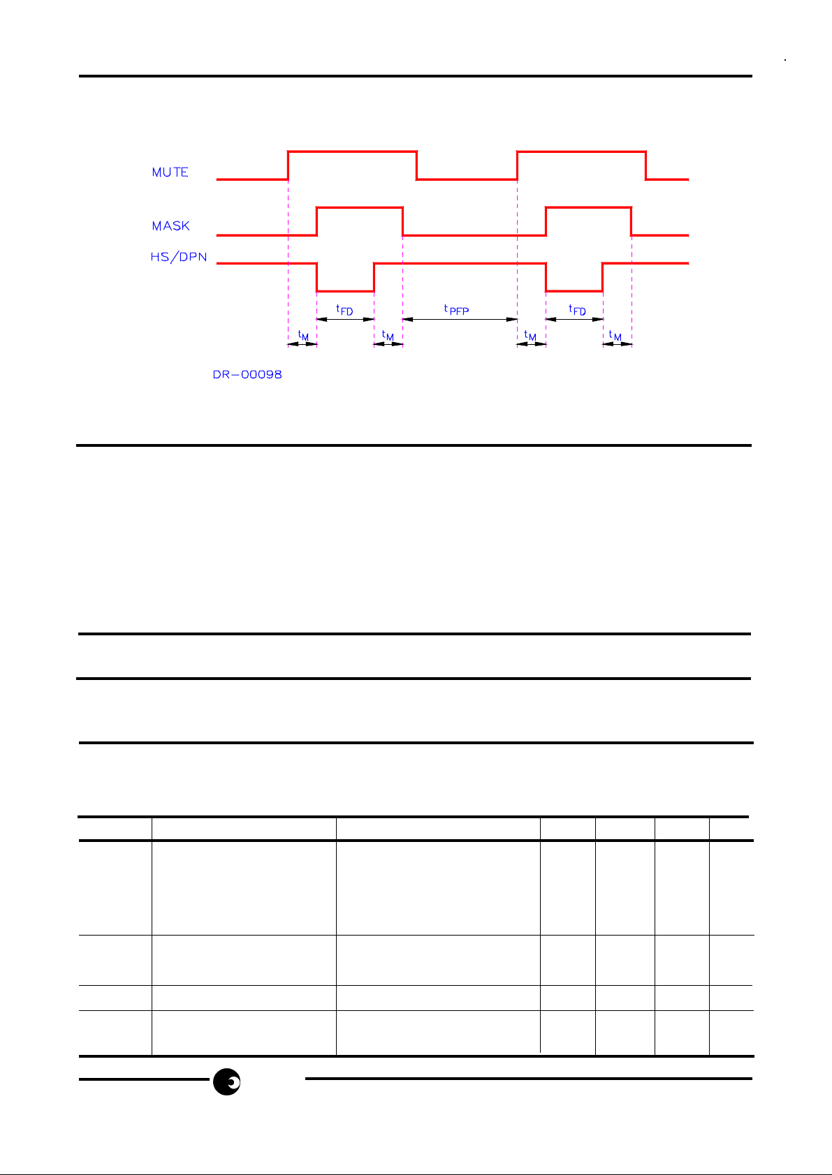
Flash
ELECTRICAL CHARACTERISTICS
Absolute Maximum Ratings
SA2531 A/B/C/E/G/U
Positive Supply Voltage ....................................................................................... -0.3V≤V
DD
≤7V
Input current .................................................................................................................. ±25mA
Input Voltage (LS) .............................................................................................. -0.3V≤VIN≤10V
Input Voltage (LI, CS) ........................................................................................... -0.3V≤V
Input Voltage (STB, RI) .............................................................................. -2V≤V
VIN≤VDD
Input Voltage (MO) ............................................................................................. -0.3V≤V
Digital Input Voltage ................................................................................... -0.3V≤V
IN≤VDD
≤8V
IN
+0.3V
≤35V
IN
+0.3V
Electrostatic Discharge ................................................................................................... ±800V
Storage Temperature ...................................................................................... -65°C to +125°C
Recommended Operating Conditions
Supply Voltage * (Speech Mode).......................................................................... 4V
≤≤
≤V
≤≤
DD
≤5V
Oscillator Frequency (Resonator: Murata CSA 3.58M G312AM).......................... 3.58 MHz
Operating Temperature ................................................................................... -25°C to +70°C
* This voltage is generated internally
DC Characteristics (I
= 15 mA unless otherwise specified)
LINE
Symbol Parameter Conditions Min Typ Max Units
I
DD
Operating Current Speech mode 3 5 m A
MF dialling 4 mA
I
DDO
V
I
OL
LD dialling V
Ring mode V
= 2.5V 200 µA
DD
= 2.5V 300 µA
DD
Retention Current Idle mode VDD = 2V, 0.05 µA
= 25°C
T
AMB
LI
Line Voltage (default) 13mA≤I
≤100mA 4.5 V
LINE
Output Current, Sink VOL = 0.4V 1.5 mA
CS,HS/DP,MO
sames
17/24
Page 18
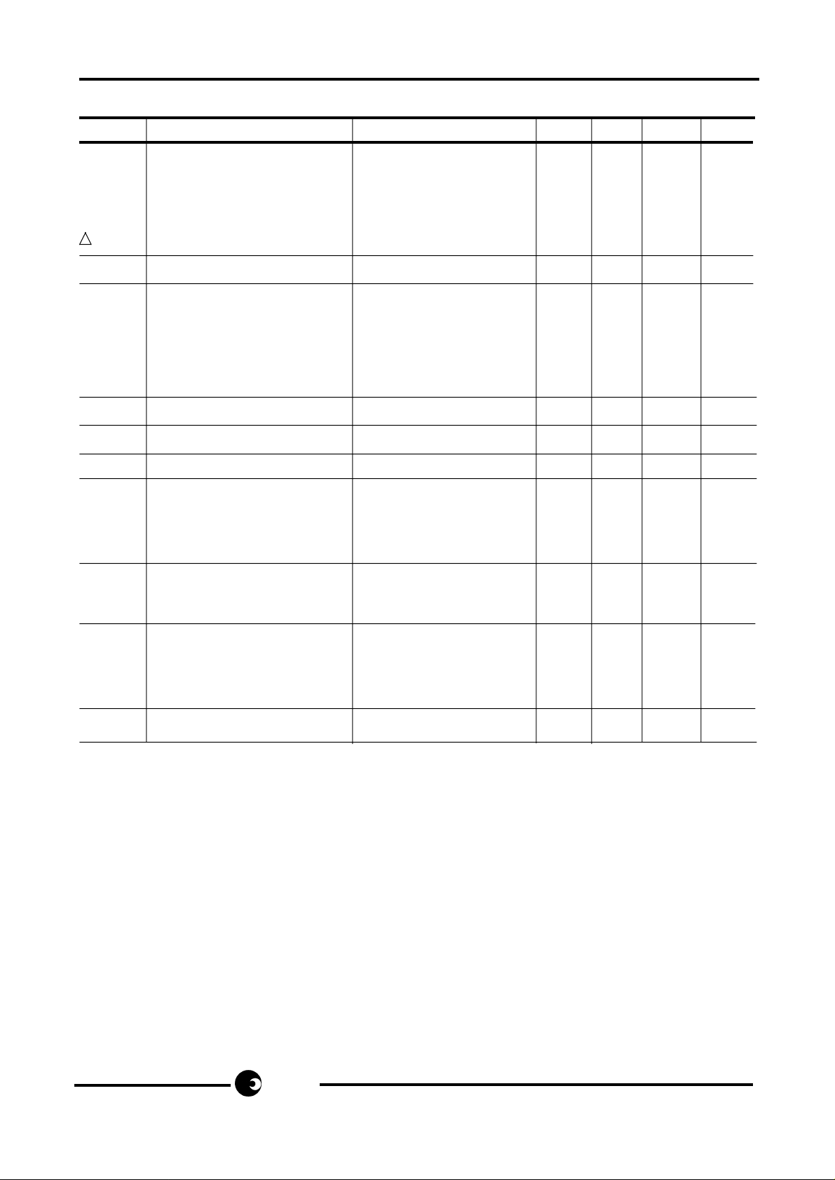
SA2531 A/B/C/E/G/U
AC Characteristics (I
=15mA;f=800Hz unless otherwise specified)
LINE
Symbol Parameter Conditions Min Typ Max Units
TX Transmit Test Circuit Fig.5
A
TX
A
TX/F
THD Distortion V
V
AGC
A
SCO
t
ATTACK
t
DECAY
Z
IN
A
MUTE
V
NO
V
FC
Gain (M1/M2) ZRL=600Ω (Α/Β/Ε/F/J) 34 35 36 dB
Z
= 1000Ω (C/D/G/v) 36.5
RL
Variation with Frequency f=500Hz to 3.4kHz ±0.8 dB
Soft Clip Level V
≤0.5V
LI
LI
RMS
=2V
2%
PEAK
Soft Clip Overdrive 20 dB
Attack Time 30 µs/6dB
Decay Time 20 ms/6dB
Input Impedance (M1/M2) 20 kΩ
Mute Attenuation Mute activated 60 dB
Noise Output Voltage -72 dBmp
Unwanted Frequency 50...300 Hz -43 dBm
Components 4.3...28 kHz note 6
above 28 kHZ -70 dBm
V
IN MAX
Input Voltage Range Differential ±1 V
(M1/M2) Single Ended ±0.5 V
PEAK
PEAK
BJT Output Driver
V
IN MAX
V
TX
Input Voltage Range (LI) ±2 V
Dynamic Range ±2 V
PEAK
PEAK
RL Return Loss ZRL = 600Ω and 1000Ω 18 dB
18/24
sames
Page 19
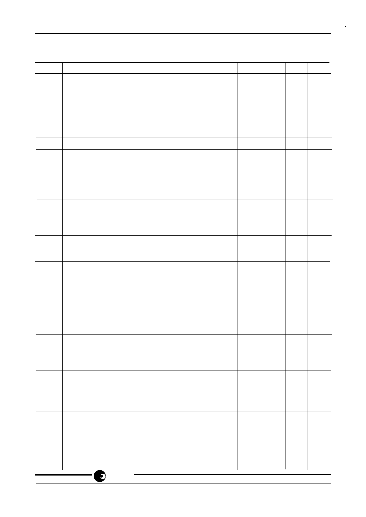
SA2531 A/B/C/E/G/U
AC Characteristics (cont’d) (I
= 15 mA;f=800Hz unless otherwise specified)
LINE
Symbol Parameter Conditions Min Typ Max Units
RX Receive Test Circuit Fig.5
A
RX
Receive Gain (RO1/RO2) ZRL=600Ω (Α/Β/Ε/F/J) 12 3dB
Z
=1000Ω (C/G/U) 0
RL
(D) 6
∆A
THD Distortion V
V
AGC
A
SCO
t
ATTACT
6dB
t
DECAY
V
NO
V
FC
Variation with Frequency f=500 Hz to 3.4 kHz ±0.8 dB
RX/F
≤0.5V
RI
RMS
Soft Clip Level VRI=1V
2%
PEAK
Soft Clip Overdrive 1 0 dB
Attact Time VRI>0.8V 30
Decay Time 20
ms/6dB
Noise Output Voltage -72 dBmp
Unwanted Frequency 50 Hz...20 kHz -60 dBm
Components
µs/
Z
V
IN RI
IN
Input Impedance (RI) 8 kΩ
Input Voltage Range(RI) ±2 V
PEAK
ST Sidetone Test Circuit Fig.5
A
V
IN ST
Z
IN
ST
Sidetone Cancellation VRI≤0.5V
RMS
Input Voltage Range (STB)
Input Impedance (STB) 80 kΩ
26 dB
±2 V
PEAK
Keyboard
t
D
Key Debounce Time 15 ms
HS Input
t
HS-L
t
HS-H
Low to High Debounce Going off-hook 15 ms
High to Low Debounce Line breaks/on-hook 240 ms
DTMF
∆ F Frequency deviation Note 5 1.2 %
V
MF
MF Tone Level(Low group)
SA2531B/D/G/U -12.5 -11 -9.5 dB
SA2531A/C/E/F/J -9.5 -8 -6.5 dB
V
V
Preemphasis Low to High SA2531A/B/C/E/F/J/U 2 .0 2.6 3.0 dB
L-H
Preemphasis Low to High SA2531D/G 2.0 2 . 6 3.2 dB
L-H
sames
19/24
Page 20
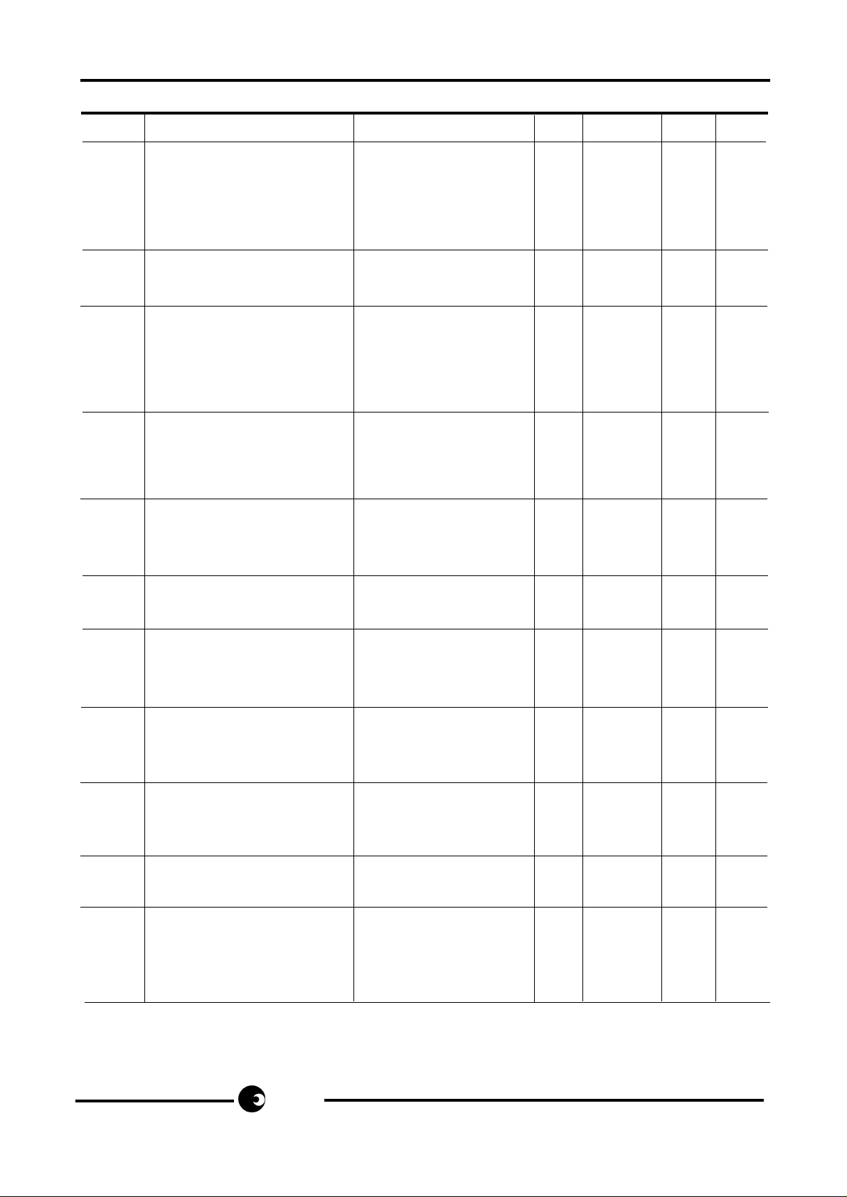
SA2531 A/B/C/E/G/U
AC Characteristics Cont'd
Symbol Parameter Conditions Min Typ Max Units
t
TD
t
ITP
t
ITP
t
TR
t
TF
t
DR
t
M/B
t
PDP
t
IDP
t
MO
t
FD
Tone Duration Note 1 80 82.3 85 ms
Inter Tone Pause SA2531A/B/C/D/F/
G/J/U Note 1 80 82.3 85 ms
Inter Tone Pause SA2531E; Note 1 160 165 170 ms
Tone Rise Time Note 2 5 ms
Tone Fall Time Note 2 5 ms
LD
Dial Rate ±5% 10 p ps
Make/Break Period ±5%, MODE=low 40.8/61.2 ms
±5%, MODE=high 33/66 ms
Pre-Digit Pause 35 ms
Inter Digit Pause 800 840 880 ms
Mute Overhang t
M
Flash Duration 1 100 102 ms
Flash Duration 2 SA2531B/CD//E/F/G 270 300 ms
Flash Duration 2 SA2531A/J/U 600 650 ms
t
PFP
Post Flash Pause SA2531 A/B/F 2.74 ms
SA2531 C/D/E/G/J/U 2.9 3.0 3.1 sec.
t
AP
t
AP
Access Pause SA2531A/B/F 2.0 2.05 2.12 sec
Access Pause SA2531C 5.8 6.0 6.2 sec
SA2531D/E/G/J/U 2.9 3.0 3.1 sec
Tone Ringer
V
t
MO
MD
Melody Output Level PDM
Melody Delay 10 ms
F1 Frequency 1 770 800 830 Hz
F2 Frequency 2 1025 1067 1110 Hz
F3 Frequency 3 1280 1333 1385 Hz
t
DT
t
TO
f
MIN
f
MIN
f
MAX
Detection Time Initial 70 80 ms
Detection Time-out note 4 ms
Min. Detection Frequency SA2531D/G 19 20 2 1 Hz
Min. Detection Frequency SA2531A/B/C/E/F/J/U 12 13 14 Hz
Max. Detection Frequency SA2531D/G 58 59 60 Hz
Max. Detection Frequency SA2531A/B/C/E/F/J/U 68 70 75 Hz
20/24
sames
Page 21
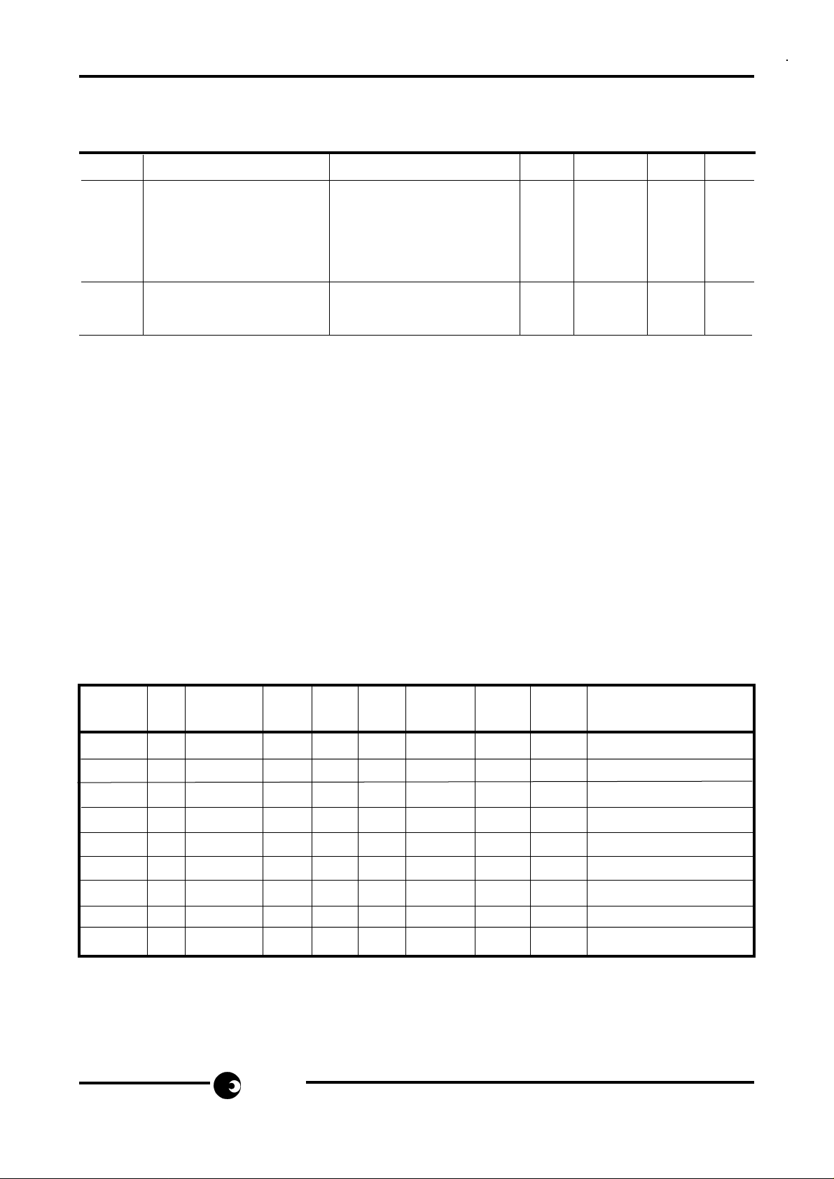
SA2531 A/B/C/E/G/U
AC Characteristics Cont'd
Symbol Parameter Conditions Min Typ Max Units
Reminder Tone
V
t
RTD
t
RTI
RT
Level (RO1/RO2) Relative to LS -30 dBr
Duration 82.3 ms
Interval 3 sec
Comfort Tone (DTMF)
V
CT
Level (RO1/RO2) Relative to LS -30 dBr
Note 1: The values are valid during automatic dialling and are minimum values during
manual dialling, i.e. the tones will continue as long as the key is depressed.
Note 2: The rise time is the time from 10% of final value till the tone amplitude has reached
90% of its final value.
Note 3: Relative to high group.
Note 4: The FCI circuit is reset by POR and HS/DP pulled high (off-hook). After a reset the
FCI circuit is in a standby state. A positive edge on FCI will start a 73 ms timer and
the frequency discrimination is initiated. Whenever a period of the ring signal is
missing, the timer is reset. When a valid ring signal is present for ≥ 73 ms, the
melody generator is started and is directly controlled by the ring signal. This
condition will remain until a new reset.
Note 5: This does not include the frequency deviation of the ceramic resonator.
Note 6: -37 dBm at 4.3 kHz and decreasing 12 dB/octave till 28 kHz.
Ordering information:
Versions ZRL DTMF FCI ITP R2 Flash in Flash Access Remarks
(W) Level (Hz) (ms) (ms) LD Mode Pause Pause
SA2531A 600 -6/-8dBm 13-70 82 600 yes 274ms 2 sec
SA2531B 600 -9/-11dBm 13-70 82 280 yes 274ms 2 sec
SA2531C 1000 -6/-8dBm 13-70 82 280 no 3 sec 6 sec
SA2531D 1000 -9/-11dBm 20-60 82 280 no 3 sec 3 sec Rx gain + 6dB, no VOL
SA2531E 600 -6/-8dBm 13-70 165 280 no 3 sec 3 sec
SA2531F 600 -6/-8dBm 13-70 82 280 yes 274 ms 2 sec MF select (*) with tone
SA2531G1000 -9/-11dBm 20-60 82 280 no 3 se c 3 s ec
SA2531J 600 -6/-8dBm 13-70 82 600 yes 3 sec 3 sec Mode pin: 10/20 pps
SA2531U 1000 -9/-11dBm 13-70 82 600 yes 3 sec 3 se c
Package styles: DIP "P" SOIC "S" PLCC "F"
Example: SA2531U in PLCC Package = SA2531UAFA
Application support:
For application support, contact your nearest SAMES Sales Office.
sames
21/24
Page 22
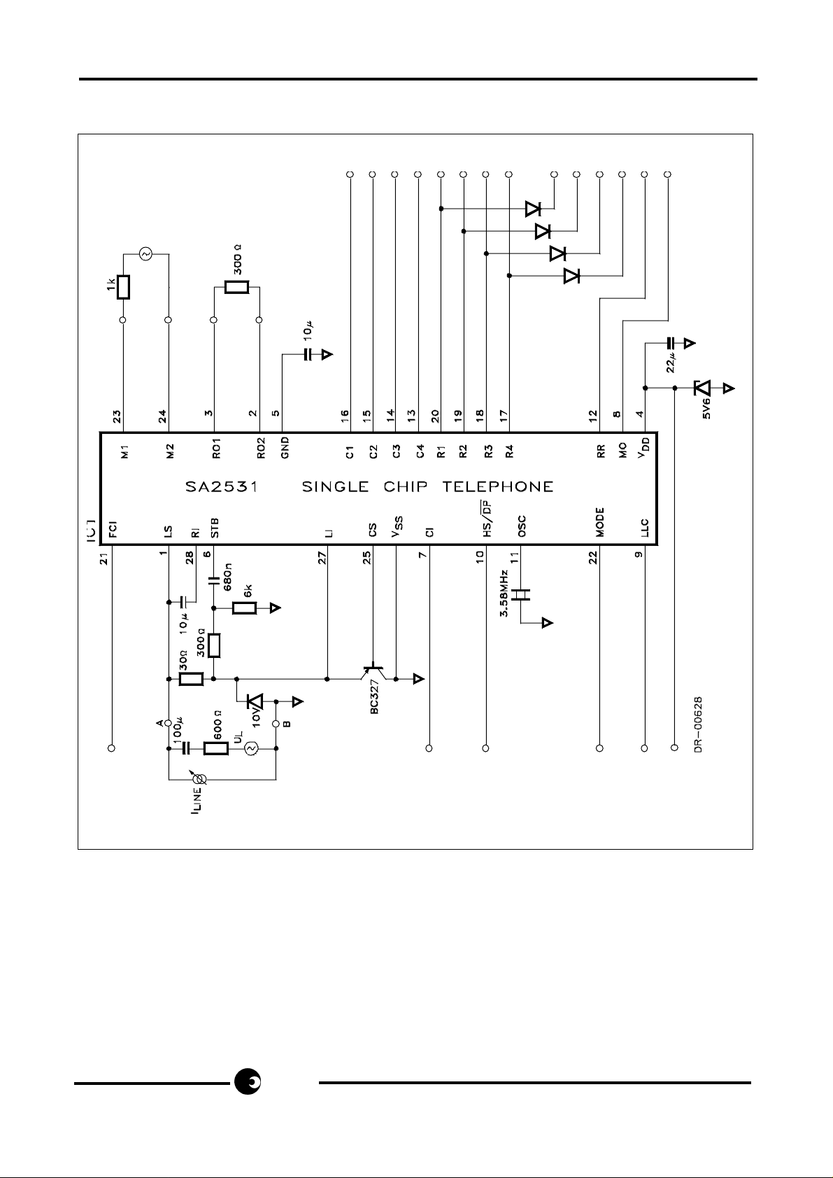
SA2531 A/B/C/E/G/U
Test Circuit
22/24
Figure 5
sames
Page 23

NOTES:
SA2531 A/B/C/E/G/U
sames
23/24
Page 24

SA2531 A/B/C/E/G/U
Disclaimer: The information contained in this document is confidential and proprietary to South African Micro-
Electronic Systems (Pty) Ltd ("SAMES) and may not be copied or disclosed to a third party, in whole or in part,
without the express written consent of SAMES. The information contained herein is current as of the date of
publication; however, delivery of this document shall not under any circumstances create any implication that
the information contained herein is correct as of any time subsequent to such date. SAMES does not undertake
to inform any recipient of this document of any changes in the information contained herein, and SAMES
expressly reserves the right to make changes in such information, without notification,even if such changes would
render information contained herein inaccurate or incomplete. SAMES makes no representation or warranty that
any circuit designed by reference to the information contained herein, will function without errors and as intended
by the designer.
South African Micro-Electronic Systems (Pty) Ltd
P O Box 15888, 33 Eland Street,
Lynn East, Koedoespoort Industrial Area,
0039 Pretoria,
Republic of South Africa, Republic of South Africa
Tel: 012 333-6021 Tel: Int +27 12 333-6021
Fax: 012 333-8071 Fax: Int +27 12 333-8071
24/24
sames
 Loading...