

Page 1
INTEGRATED CIRCUITS
SA2420
Low voltage RF transceiver — 2.45GHz
Product specification 1997 May 23
Page 2
Philips Semiconductors Product specification
SA2420Low voltage RF transceiver — 2.45 GHz
DESCRIPTION
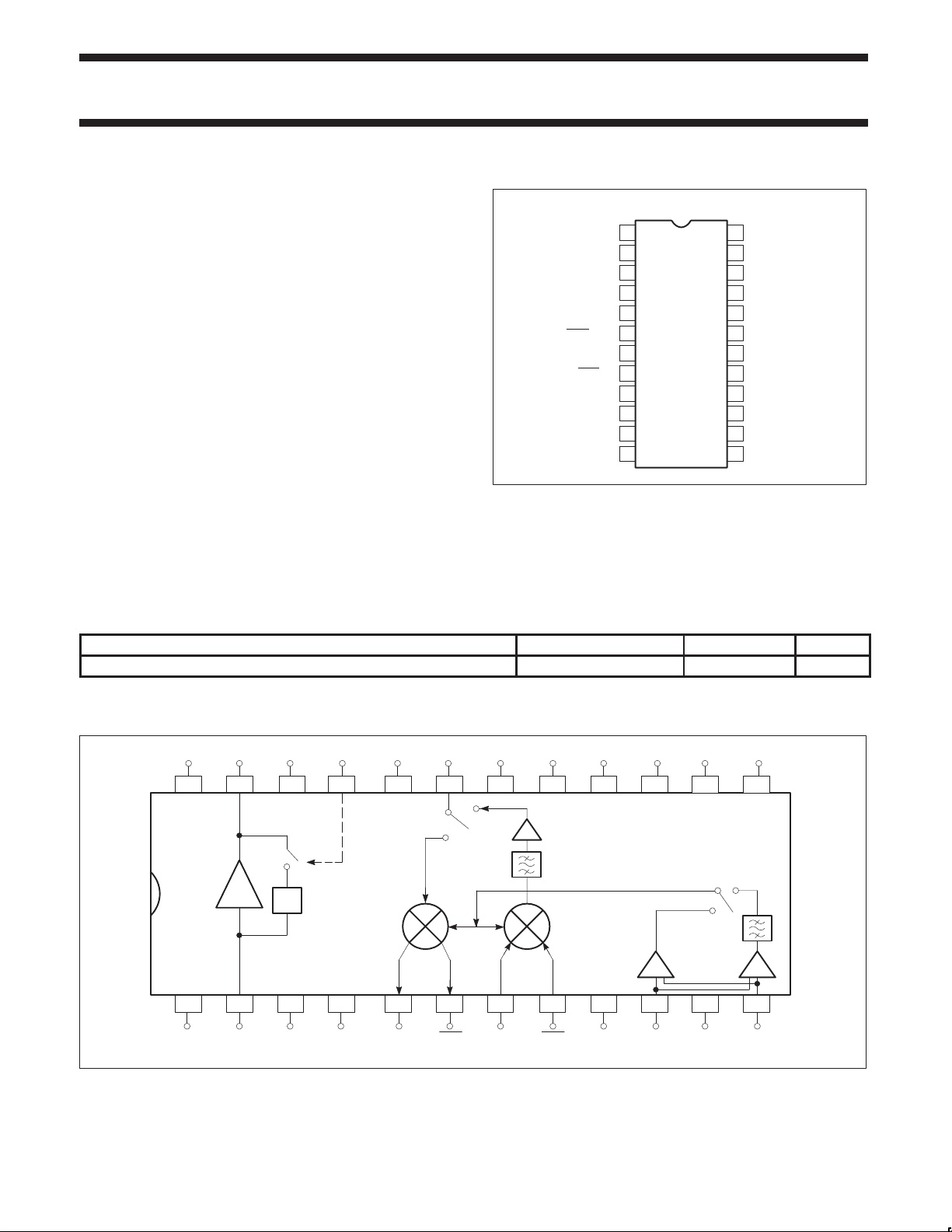
The SA2420 transceiver is a combined low-noise amplifier, receive
mixer, transmit mixer and LO buf fer IC designed for
high-performance low-power communication systems for
2.4-2.5GHz applications. The LNA has a 2.5dB noise figure at
2.45GHz with 14dB gain and an IP3 intercept of -3dBm at the input.
The gain is stabilized by on-chip compensation to vary less than
±0.2dB over the -40 to +85°C temperature range. The
wide-dynamic-range receive mixer has a 10.9dB noise figure and an
input IP3 of +2.8dBm at 2.45GHz. The nominal current drawn from
a single 3V supply is 37mA in transmit mode and 22mA in receive
mode.
FEATURES
•Low current consumption: 37mA nominal transmit mode and
22mA nominal receive mode
•Fabricated on a high volume, rugged BiCMOS technology
•High system power gain: 22.5dB (LNA + Mixer) at 2.45GHz
•TSSOP24 package
•Excellent gain stability versus temperature and supply voltage
•-10dBm LO input power can be used to drive the mixer
•Operates with either full or half frequency LO
•Wide IF range: 50–500MHz
ORDERING INFORMATION
DESCRIPTION TEMPERATURE RANGE ORDER CODE DWG #
24-Pin Plastic Thin Shrink Small Outline Package (Surface-mount, TSSOP)
PIN CONFIGURATION
DH Package
GND
1
LNA IN
2
GND
3
4
GND
OUT
GND
LOP
LO SW
LOM
5
6
7
IN
8
9
10
11
12
Rx IF OUT
Rx IF
Tx IF IN
Tx IF
Figure 1. Pin Configuration
APPLICATIONS
•2.45GHz WLAN front-end (802.11, ISM)
-40 to +85°C
SA2420DH SOT355-1
24
V
LNA OUT
23
GND
22
ATTEN SW
21
GND
20
19
RF IN/OUT
GND
18
Tx/Rx SW
17
GND
16
GND
15
14
V
CHIP EN
13
SR00164
CC
CC
LO
BLOCK DIAGRAM
V
CC
24 23 22 21 20
GND GND
LNA
OUT
LNA
LNA
IN
GND
ATTENUATOR
ATTEN
SW
GND
RF IN/
OUT GND
GND
Tx/Rx
SW GND
19 18 17 16 15
TX
PRE-DRIVER
BPF
RX
RX TX
43215
GND
Rx IF
OUT
Rx IF
OUT
761098
Tx IFINTx IF
IN
Figure 2. SA2420 Block Diagram
BUFFER
V
LO
CHIP
CC
14 13
BPF
FREQ.
DBLER
1211
LOGND LOP
SW
LOM
EN
X2X1
SR00165
1997 May 23 853–1984 18069
2
Page 3
Philips Semiconductors Product specification
SYMBOL
PARAMETER
TEST CONDITIONS
UNITS
SA2420Low voltage RF transceiver — 2.45 GHz
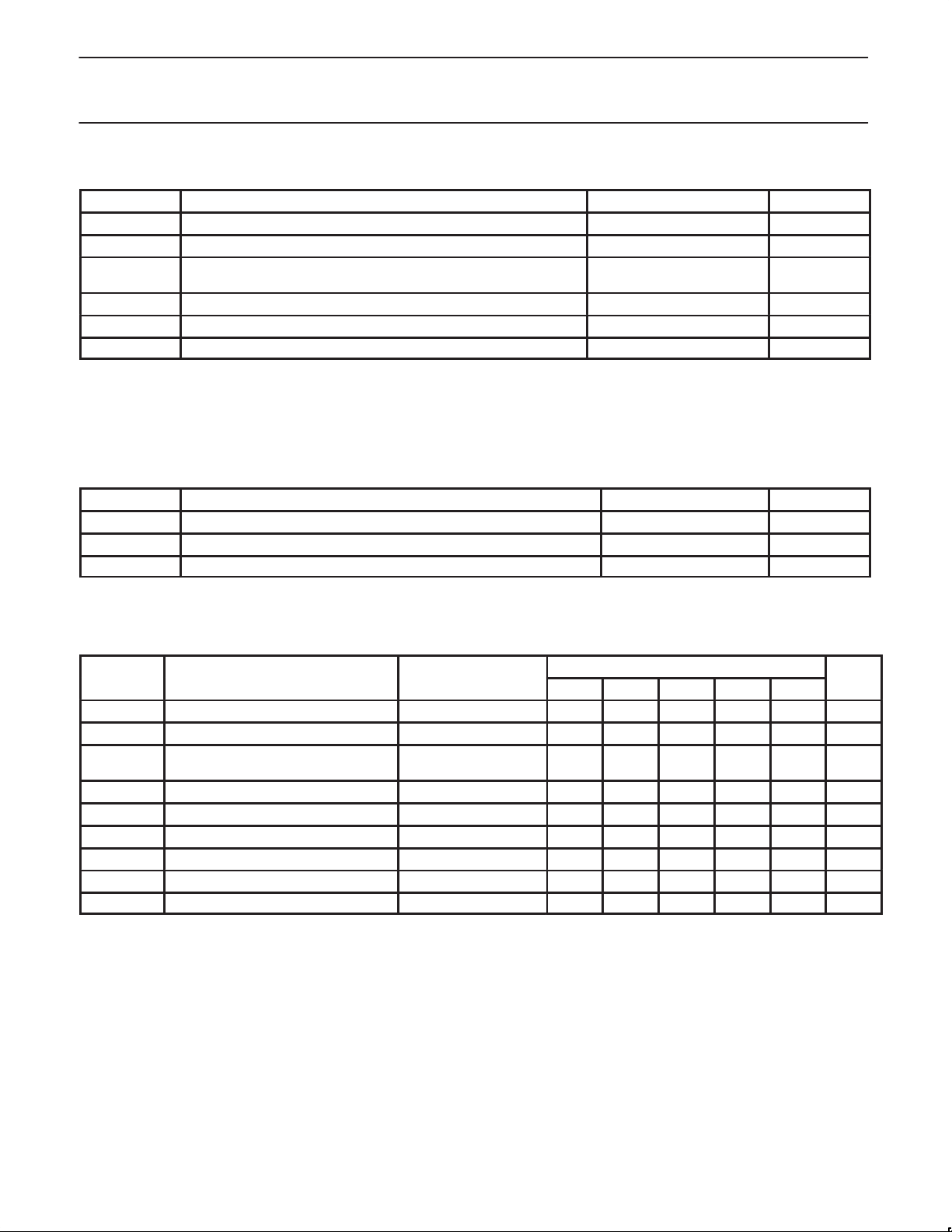
ABSOLUTE MAXIMUM RATINGS
SYMBOL PARAMETER RATING UNITS
V
CC
V
IN
P
D
T
JMAX
P
MAX
T
STG
NOTE:
1. Transients exceeding these conditions may damage the product.
2. Maximum dissipation is determined by the operating ambient temperature and the thermal resistance, and absolute maximum ratings may
impact product reliability θ
3. IC is protected for ESD voltages for 2000V , excepts pins 10 and 12, which are protected up to 500V.
RECOMMENDED OPERATING CONDITIONS
SYMBOL PARAMETER RATING UNITS
V
CC
T
A
T
J
Supply voltage -0.3 to +6 V
Voltage applied to any pin -0.3 to (VCC + 0.3) V
Power dissipation, TA = 25°C (still air)
24-Pin Plastic TSSOP
555
mW
Maximum operating junction temperature 150 °C
Maximum power (RF/IF/LO pins) +20 dBm
Storage temperature range –65 to +150 °C
: 24-Pin TSSOP = 117°C/W
JA
Supply voltage 2.7 to 5.5 V
Operating ambient temperature range -40 to +85 °C
Operating junction temperature -40 to +105 °C
DC ELECTRICAL CHARACTERISTICS
VCC = +3V, TA = 25°C; unless otherwise stated.
I
CCTX
I
CCRX
I
CC OFF
V
LNA-IN
I
LNA-OUT
V
LO 2.1 GHz
V
LO 1.05 GHz
V
TX IF
V
TX IFB
Supply current, Transmit LO mode = Hi 25 37 45 mA
Supply current, Receive LO mode = Hi 15 22 28 mA
Power down mode (Tx/Rx SW = Low)
LNA input voltage Receive mode 0.855 V
LNA output bias current Receive mode 4.0 mA
LO buffer DC input voltage LO mode = Hi 2.1 V
LO buffer DC input voltage LO mode = Low 2.1 V
Tx Mixer input voltage Transmit mode 1.7 V
Tx Mixer input voltage Transmit mode 1.7 V
LO mode = Hi,
LNA gain = Hi
LIMITS
MIN -4σ TYP +4σ MAX
0 10 µA
1997 May 23
3
Page 4
Philips Semiconductors Product specification
SYMBOL
PARAMETER
TEST CONDITIONS
UNITS
SA2420Low voltage RF transceiver — 2.45 GHz
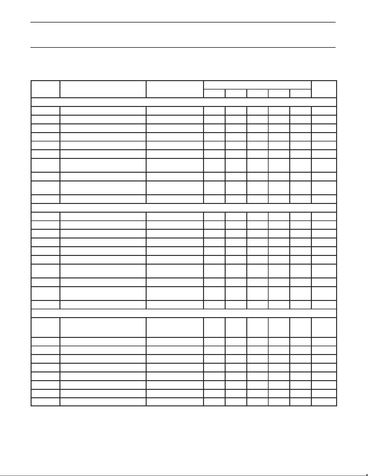
AC ELECTRICAL CHARACTERISTICS
VCC = +3V, TA = 25°C; LOIN = -10dBm @ 2.1GHz; fRF = 2.45GHz; unless otherwise stated.
LIMITS
MIN -4σ TYP +4σ MAX
Low Noise Amplifier (In = Pin 2; Out = 23)
S
∆S21/∆T Gain temperature sensitivity LNA gain = Hi -0.002 dB/°C
∆S21/∆VCCGain VCC drift LNA gain = Hi 0.3 dB/V
S
S
S
ISO Isolation: LO1 to LNA
P
-1dB
IP3 Amplifier input third order intercept
NF Amplifier noise figure (50Ω) LNA gain = Hi 2.3 2.5 2.7 dB
LNA High Overload Mode
S
∆S21/∆T Gain temperature sensitivity LNA gain = Low -0.01 dB/°C
∆S21/∆VCCGain VCC drift LNA gain = Low 0.3 dB/V
S
S
S
ISO Isolation: LO1 to LNA
P
-1dB
IP3 Amplifier input third order intercept
NF Amplifier noise figure (50Ω) LNA gain = Low 17 dB
Rx Mixer (RF = Pin 19, IF = Pins 5 and 6, LO = Pin 10 or 12, PLO = -10dBm)
PG
∆GC/∆T Gain temperature drift -0.016 dB/°C
∆GC/∆VCCGain VCC drift 0.34 dB/V
S
11–RF
NF
P
-1dB
IP3 Input third order intercept f1 - f2 = 1MHz 1.7 2.8 3.9 dBm
f
RF
f
Amplifier gain LNA gain = Hi 12.7 14.0 15.3 dB
21
Amplifier reverse isolation LNA gain = Hi -22 dB
12
Amplifier input match
11
Amplifier output match
22
1
1
IN
LNA gain = Hi -8 dB
LNA gain = Hi -8 dB
LO mode = Hi,
LNA gain = Hi
-45 dB
Amplifier input 1dB gain compression LNA gain = Hi -15 dBm
f1 - f2 = 1MHz,
LNA gain = Hi
Amplifier gain LNA gain = Low –14.0 -13.3 –12.0 dB
21
Amplifier reverse isolation LNA gain = Low -16 dB
12
Amplifier input match
11
Amplifier output match
22
1
1
IN
LNA gain = Low -8 dB
LNA gain = Low -8 dB
LO mode = Hi,
LNA gain = Low
-3 dBm
-45 dB
Amplifier input 1dB gain compression LNA gain = Low +6 dBm
f1 - f2 = 1MHz,
LNA gain = Low
Power conversion gain into 50Ω :
matched to 50W using external balun
C
circuitry.
Input match at RF (2.45GHz)
SSB noise figure (2.45GHz) (50Ω) 10.2 10.9 11.6 dB
M
1
fS = 2.45GHz,
fLO = 2.1GHz,
f
= 350MHz
IF
7.9 8.5 9.1 dB
17 dBm
-15 dB
Mixer input 1dB gain compression –11.4 -10.3 –9.2 dBm
RF frequency range
IF frequency range
IF
3
3
2.4 2.45 2.5 GHz
300 350 400 MHz
1997 May 23
4
Page 5

Philips Semiconductors Product specification
SYMBOL
PARAMETER
TEST CONDITIONS
UNITS
SA2420Low voltage RF transceiver — 2.45 GHz
AC ELECTRICAL CHARACTERISTICS (continued)
LIMITS
MIN -4σ TYP +4σ MAX
Rx Mixer Spurious Components (PIN = P
P
P
RF-IF
LO-IF
RF feedthrough to IF CL = 2pF per side -35 dBc
LO feedthrough to IF CL = 2pF per side -35 dBc
Tx Mixer (RF = Pin 19, IF = Pins 7 and 8, LO = Pin 10 or 12, PLO = -10dBm)
PG
Power conversion gain: RL = 50Ω
C
RS = 50Ω
∆GC/∆T Gain temperature drift -0.032 dB/°C
∆GC/∆VCCGain voltage drift 0.4 dB/V
S
NF
P
11–RF
-1dB
Output match at RF (2.45GHz)
SSB noise figure (2.45GHz) (50Ω) 13.2 dB
M
Output 1dB gain compression 1.5 2.9 4.3 dBm
IP3 Output third order intercept f1 - f2 = 1MHz 10.1 +11.5 12.9 dBm
f
RF
f
RF frequency range
IF frequency range
IF
Tx Mixer Spurious Components (P
P
IF-RF
P
LO-RF
P
2LO-RF
P
IMAGE-RF
IF feedthrough to RF -29 dBc
LO feedthrough to RF -20 dBc
2*LO feedthrough to RF -25 dBc
Image feedthrough to RF -0 dBc
3
3
OUT
LO Buffer: Full and Half Frequency inputs
P
S
11-LO1
S
11-LO2
f
LO2G
f
LO1G
Switching
t
Rx-Tx
t
Tx-Rx
t
POWER UP
t
PWR DWN
LO drive level (see figure 16) -10 -7 5 dBm
LO
Mixer input match (LO = 2.1GHz) LO mode = Hi -10 dB
Mixer input match (LO = 1.05GHz) LO mode = Low -10 dB
LO2G frequency range
LO1G frequency range
2
3
3
Receive-to-transmit switching time 1 µs
Transmit-to-Receive switching time 1 µs
Chip enable time 1 µs
Chip disable time 1 µs
NOTES:
1. With simple external matching
2. With 50pF coupling capacitors on all RF and IF parts
3. This part has been optimized for the frequency range at 2.4–2.5 GHz. Operation outside this frequency range may yield performance other
than specified in this datasheet.
= P
-1dB
1
-1dB
)
fS = 2.45GHz,
fLO = 2.1GHz,
15.0 17 19.9 dB
fIF = 350MHz
-10 dB
2.4 2.45 2.5 GHz
300 350 400 MHz
)
LO mode = Hi 1.9 2.1 2.3 GHz
LO mode = Low 0.85 1.05 1.25 GHz
1997 May 23
5
Page 6
Philips Semiconductors Product specification
SA2420Low voltage RF transceiver — 2.45 GHz
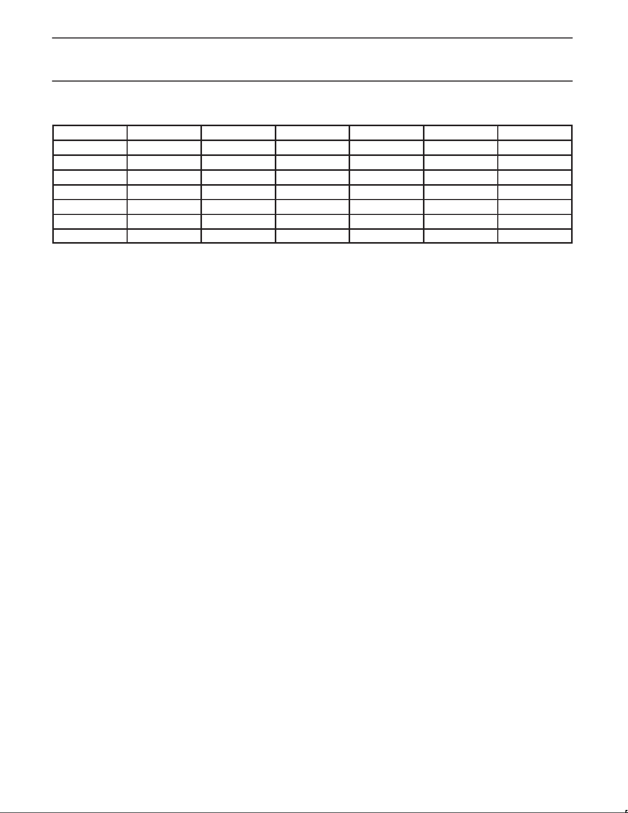
Table 1. Truth Table
Chip-En TxRx-SW LNA-SW LO-SW Mode LNA Gain LO Freq. (Typ)
0 X X X Sleep N/S N/S
1 0 1 1 Receive +14dB 2.1GHz
1 0 0 1 Receive -8dB 2.1GHz
1 0 1 0 Receive +14dB 1.05GHz
1 0 0 0 Receive -8dB 1.05GHz
1 1 X 1 Transmit N/S 2.1GHz
1 1 X 0 Transmit N/S 1.05GHz
FUNCTIONAL DESCRIPTION
The SA2420 is a 2.45GHz transceiver front-end available in the
TSSOP-24 package. This integrated circuit (IC) consists of a low
noise amplifier (LNA) and up- and down-converters. The injection of
the local oscillator (LO) signal has two options: 1) direct injection of
the LO signal at approximately 2GHz, or 2) injection of an LO signal
at approximately 1GHz through an on-chip doubler. The SA2420
functions with a supply voltage range of 3 – 5 V (nominally). There
is an enable/disable switch available to power up/down the entire
chip in 1µs, typically. This transceiver has several unique features.
The LNA has two operating modes: 1) high gain mode with a gain =
+14dB; and 2) low gain mode with a gain <-10dB. The switch for
this option is internal and is controlled externally by high and low
logic to the pin. When the LNA is switched into the attenuation
mode, active matching circuitry (on-chip) is switched in (reducing the
number of off-chip components required). To reduce power
consumption when the chip is transmitting, the LNA is automatically
switched into a “sleep” mode (internally) without the use of external
circuitry.
The up and down frequency converters are single-ended at the RF
port of the mixers. The up and down converters share the same
(RF) pin and use an internal switch for transmitting (up-converting)
or receiving (down-converting) modes. The switch is controlled
externally by high and low logic states. The RF port is matched to
50Ω and has an input IP3 of +2.8dBm (mixer only). The
down-convert mixer is buffered and has open collectors at the pins
to allow for matching to common SAW filters. The up-convert mixer
has differential inputs (IF port) and single-ended output (RF port),
with an input pin to output pin gain of 17dB. The output of the
up-converter is designed for a power level = +3dBm (P
mixers are fed by the two LO options.
The available LO options are: direct injection (2.1GHz at the pin) or
through an on-chip doubler . The doubler has a simple LC bandpass
filter (internal) at its output which passes the second harmonic to the
mixers. Through an internal switch (controlled externally), either LO
can be used depending on the designer’s application. If an
application requires the use of a 1.05GHz VCO, then the doubler
option would be used to double the frequency (2 × 1.05GHz =
2.1GHz) before being injected into the mixers. For a 2.1GHz VCO,
the direct option would be used. With this option, the signal passes
through an on-chip buffer and is then injected into the mixers.
-1dB
). The
1997 May 23
6
Page 7
Philips Semiconductors Product specification
SA2420Low voltage RF transceiver — 2.45 GHz
50
Vcc = 3V
40
30
CURRENT (mA)
20
10
–50 0 50
TEMPERATURE (°C)
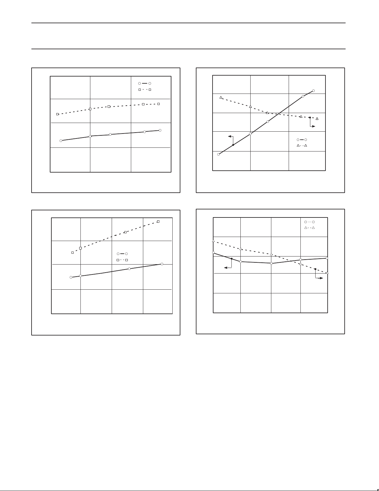
Figure 3. Rx & Tx Currents VS Temperature
50
T = 25°C
40
30
CURRENT (mA)
20
NF
GAIN
14.8
14.4
14.0
13.6
13.2
12.8
100
SR01460
GAIN (dB)
R
X
T
X
SR01458
100
3.0
Vcc = 3V
2.8
2.6
2.4
NOISE FIGURE (dB)
2.2
2.0
–50 0 50
TEMPERATURE (°C)
Figure 5. LNA Gain & 50W NF VS Temperature
3.0
Vcc = 3V
2.8
R
X
T
X
2.6
2.4
NOISE FIGURE (dB)
2.2
NF
GAIN
14.8
14.4
14.0
13.6
13.2
GAIN (dB)
10
23 5
4
VOLTS (V)
Figure 4. Rx & Tx Currents VS Voltage Supply
1997 May 23
SR01459
2.0
6
2.400 2.425 2.450
FREQUENCY (GHz)
2.475
12.8
2.500
SR01461
Figure 6. LNA Gain & 50W NF VS Frequency
7
Page 8
Philips Semiconductors Product specification
SA2420Low voltage RF transceiver — 2.45 GHz
3.0
T = 25°C
2.8
2.6
2.4
NOISE FIGURE (dB)
2.2
2.0
23 4
VOLTS (V)
5
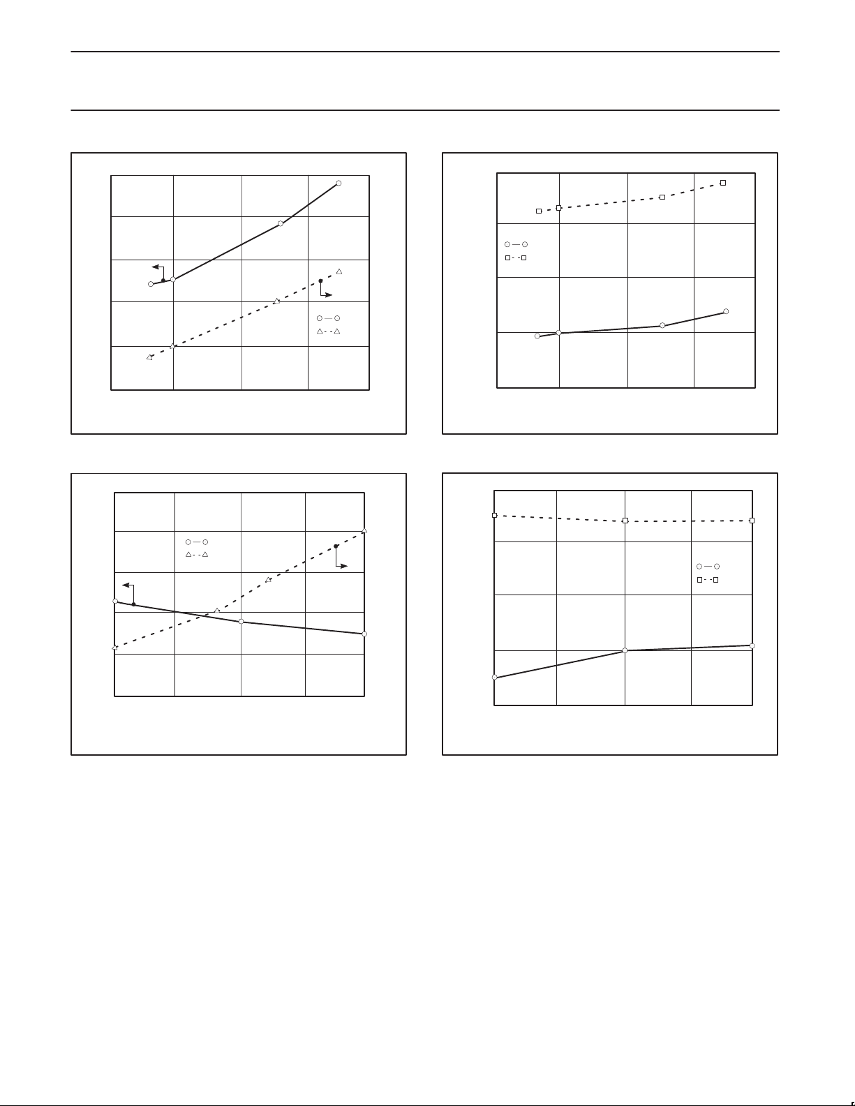
Figure 7. LNA Gain & 50W NF VS Supply Voltage
–12.0
T = 25°C
V
= 3V
cc
–12.4
–12.8
–13.2
S21 LOSS (dB)
LOSS
S12
NF
GAIN
18
17
16
15
14
13
6
SR01462
–23.0
–23.8
–24.6
–25.4
GAIN (dB)
S12(dB)
0
T = 25°C
–5
P–1dB
IP3
–10
–15
INPUT IP3 AND 1 dB GAIN COMPRESSION (dBm)
–20
23 4
VOLTS (V)
5
SR01464
Figure 9. LNA Input IP3 and P–1dB VS Supply Voltage
0
–5
P–1dB
IP3
–10
6
–13.6
–14.0
2.400 2.425 2.450
FREQUENCY (GHz)
2.475
Figure 8. LNA Loss Mode & S12 VS Frequency
–26.2
–27.0
2.500
SR01463
–15
Input IP3 and 1 dB Gain compression (dBm)
–20
2.400 2.425 2.450
FREQUENCY (GHz)
Vcc = 3VT = 25°C
2.475
Figure 10. LNA Input IP3 and P–1dB VS Frequency
2.500
SR01465
1997 May 23
8
Page 9
Philips Semiconductors Product specification
SA2420Low voltage RF transceiver — 2.45 GHz
20
15
P–1dB
IP3
10
5
LNA LOSS MDOE INPUT IP3 AND P–1dB (dBm)
0
23 4
VOLTS (V)
T = 25°C
5
6
SR01466
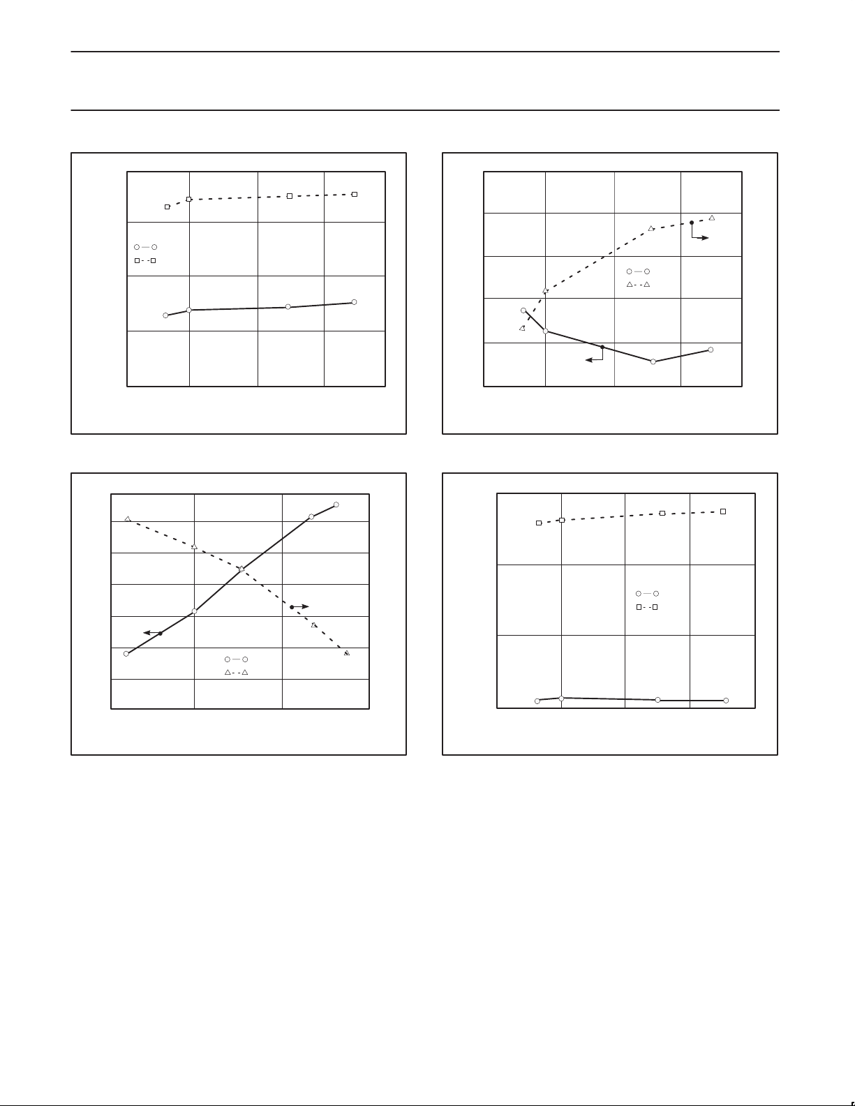
Figure 11. LNA Loss Mode Input IP3 and P–1dB VS Voltage
11.8
11.4
11.0
10.6
10.2
9.8
SSB NOISE FIGURE (dB)
9.4
9.0
–50 0
VCC = 3V
NF
GAIN
50
TEMPERATURE (°C)
9.8
9.4
9.0
8.6
8.2
7.8
7.4
7.0
100
SR01467
Figure 12. Rx Mixer Conv. Gain & SSB NF VS Temperature
11.5
11.3
11.1
10.9
SSB NOISE FIGURE (dB)
10.7
10.5
23 4
Figure 13. Rx Mixer Conv. Gain & SSB NF VS Supply Voltage
–5
CONVERSION GAIN (dB)
INPUT IP3 AND 1 dB GAIN COMPRESSION (dBm)
–10
Figure 14. Rx Mixer Input IP3 and P–1dB VS Supply Voltage
T = 25°C
VOLT (V)
5
T = 25°C
0
23 4
VOLTS (V)
NF
GAIN
P–1dB
IP3
10.0
9.6
9.2
8.8
CONVERSION GAIN (dB)
8.4
5
5
8.0
6
SR01468
SR01469
6
1997 May 23
9
Page 10
Philips Semiconductors Product specification
SA2420Low voltage RF transceiver — 2.45 GHz
5
0
V
3V
CC =
T = 25°C
–5
INPUT IP3 AND 1 dB GAIN COMPRESSION (dBm)
–10
2.400 2.425 2.450
FREQUENCY (GHz)
P–1dB
IP3
2.475
2.500
SR01470
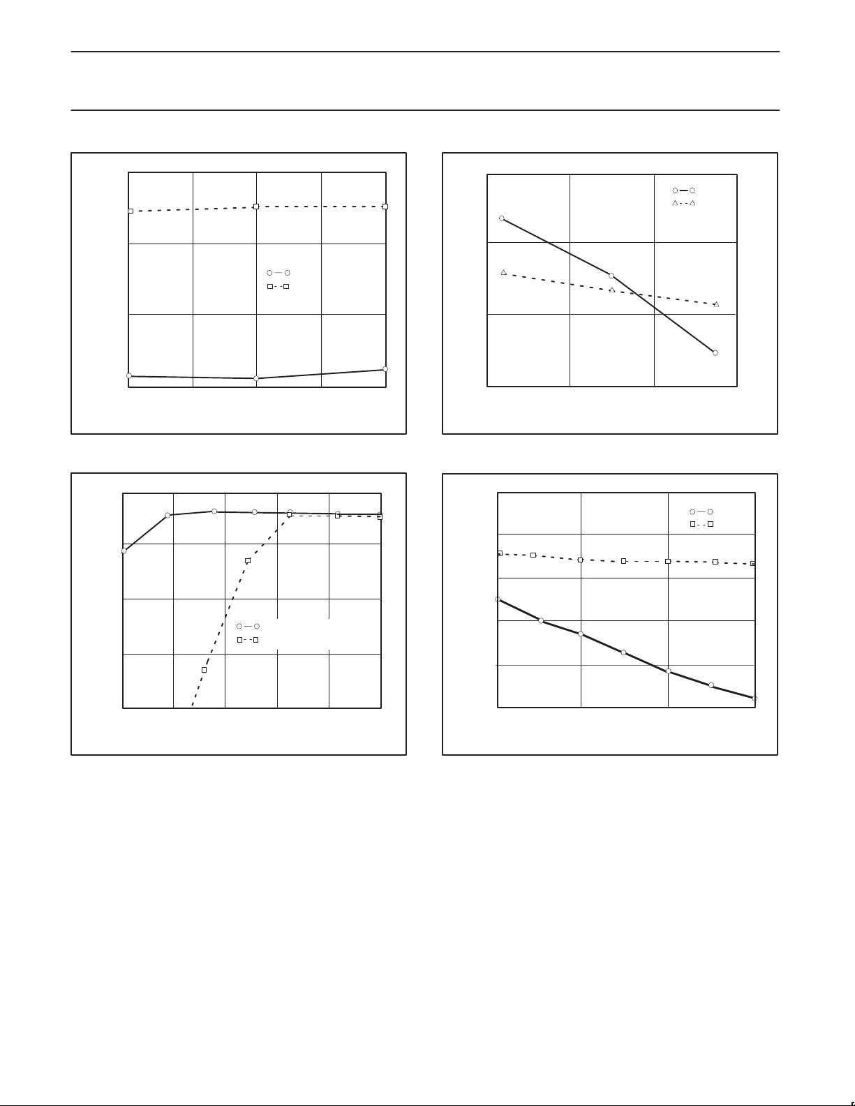
Figure 15. Rx Mixer Output IP3 and P–1dB VS Frequency
10
5
0
FULL (LO = 2.1 GHZ)
DOUBLER (LO = 1.05 GHZ
–5
Rx MIXER CONVERSION GAIN (dB)
22
20
CURRENT (mA)
18
VCC = 3V
16
–50 0 50
TEMPERATURE (°C)
12
GAIN
POWER
6
0
–6
100
SR01472
Figure 17. Tx Mx conv . Gain and Output Pwr VS Temp.
0
LO
–6
–12
–18
–24
LO AND IMAGE SUPPRESSION (dbc)
IMAGE
SATURATED OUTPUT POWER (dB)
–10
–30 –24 –18
LO POWER (dBM)
–12
Figure 16. Rx Mixer Conversion Gain VS LO Power
1997 May 23
–30
–6
0
SR01471
–30 –20
LO POWER (dBM)
–10
0
SR01473
Figure 18. Tx Mixer LO and Image Suppression
10
Page 11
Philips Semiconductors Product specification
SA2420Low voltage RF transceiver — 2.45 GHz
13.8
13.6
T = 25°C
13.4
13.2
NF
SSB NOISE FIGURE (dB)
13.0
12.8
23
4
VOLTS (V)
GAIN
5
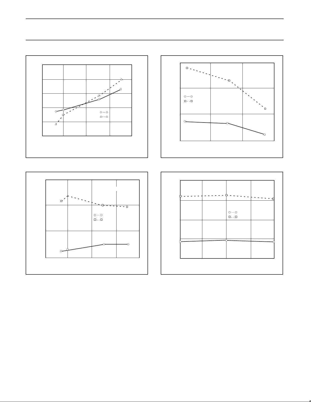
Figure 19. Tx Mixer Gain & NF VS Supply Voltage
15
T = 25°C
10
P–1dB
IP3
21.0
20.4
19.8
19.2
CONVERSION GAIN (dB)
18.6
18.0
6
SR01474
16
VCC = 3V
10
P–1dB
IP3
4
OUTPUT IP3 AND 1 dB GAIN COMPRESSION (dBm)
–2
–50 0
TEMPERATURE (°C)
50
100
SR01479
Figure 21. Tx Mixer Output IP3 and P–1dB VS Temperature
12
9
V
= 3V
6
CC
T = 25°C
P–1dB
IP3
5
OUTPUT P–1dB AND IP3 (dBM)
0
23
4
VOLTS (V)
5
SR01475
Figure 20. Tx Mixer Output P–1dB and IP3 Vs Voltage
3
OUTPUT IP3 AND 1 DB GAIN COMPRESSION (dBm)
6
0
2.400 2.425
2.450
FREQUENCY (GHz)
2.475
2.500
SR01480
Figure 22. Tx Mixer Output IP3 and P–1dB VS Frequency
1997 May 23
11
Page 12
Philips Semiconductors Product specification
SA2420Low voltage RF transceiver — 2.45 GHz
20
GND
145
19
RF I/O
RF I/O
C14
C13
260
33pF
1.5pF
18
GND
SW4
17
Tx/Rx SW
16
GND
15
GND
C11
SW3
CC
V
33pF
14
LO
CC
V
C12
100nF
SW2
13
ENABLE
LNA OUT
CC
C18
(not used)
22
GND
SW5
V
L4
21
ATTEN SW
100nH
C15
1.5pF
+
C17
10uF
CC
V
C16
100nF
V
24
CC
200
23
LNA OUT
SA2420
GND
LNA IN
GND
GND
Rx IF OUT
Rx IF OUT
Tx IF IN
Tx IF IN
GND
LOP
LO SW
U1
1
2
3
4
5
6
7
8
9
10
LOM
11
12
RF TRANSCEIVER
2.45 GHz LOW VOLTAGE
C1
1.5pF
300
300
300
300
TxIN
(352 MHz)
L3
C8
C7
10pF
33nH
10pF
C2
1.5pF
C3
10pF
L1
47nH
CC
V
LNA IN
L2
27nH
C4
RxOUT
(352 MHz)
3.3pF
C5
10pF
C6
100pF
C9
33pF
R1
SW1
C10
33pF
W
50
L0
CC
V
GND
THICK OF NATURAL FR–4 SUBSTRATE
: 10 MILS WIDE, XXX MILS LONG ON 31 MILS
XXX
SR01481
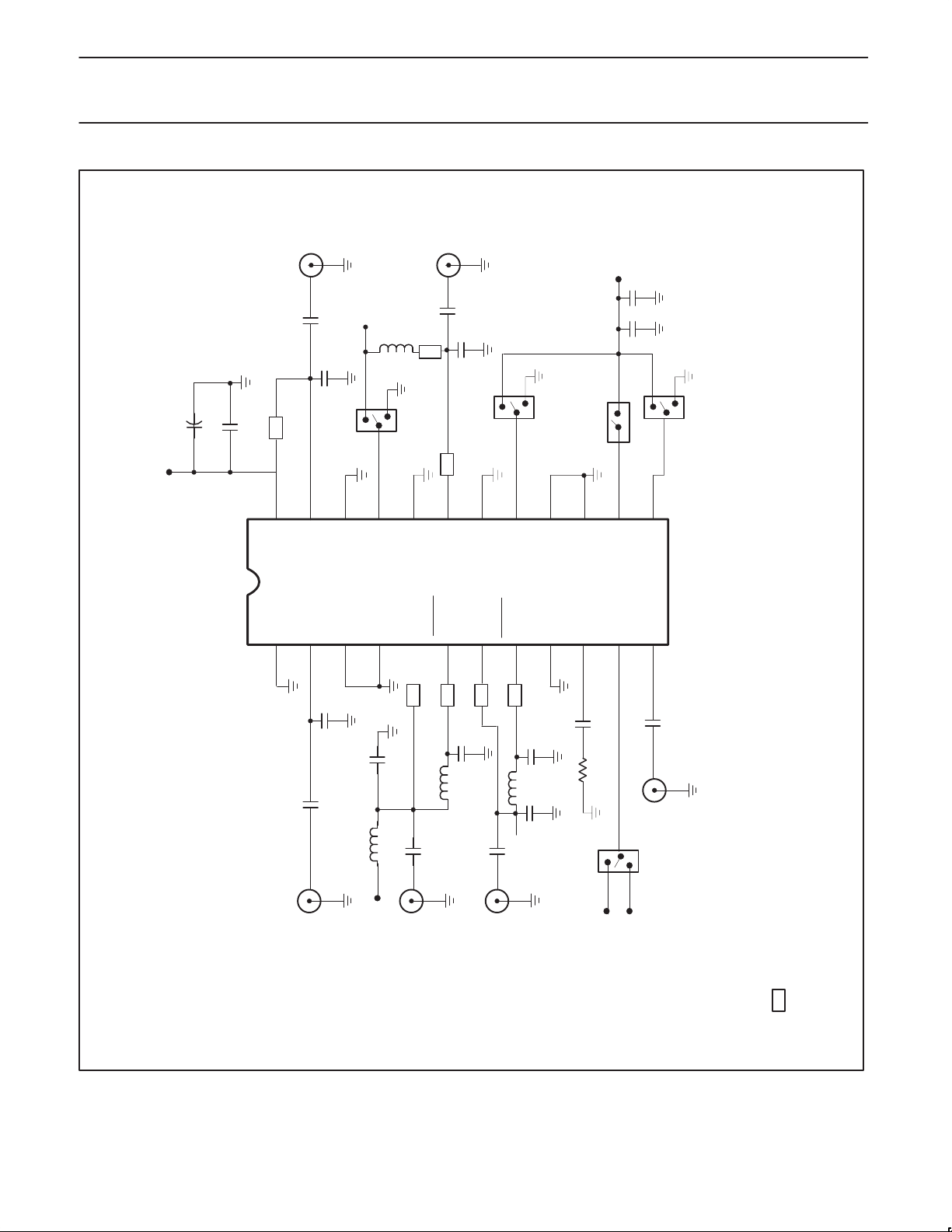
Figure 23.
1997 May 23
12
Page 13
Philips Semiconductors Product specification
SA2420Low voltage RF transceiver — 2.45 GHz
1997 May 23
SR01485
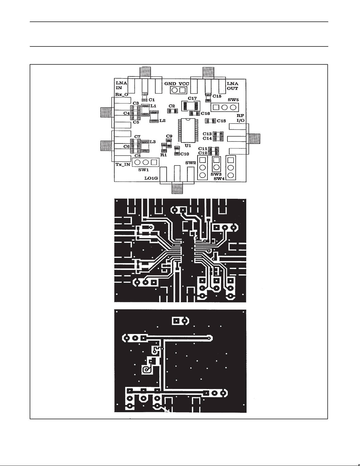
Figure 24. SA2420 RF Transciever
13
Page 14
Philips Semiconductors Product specification
SA2420Low voltage RF transceiver — 2.45GHz
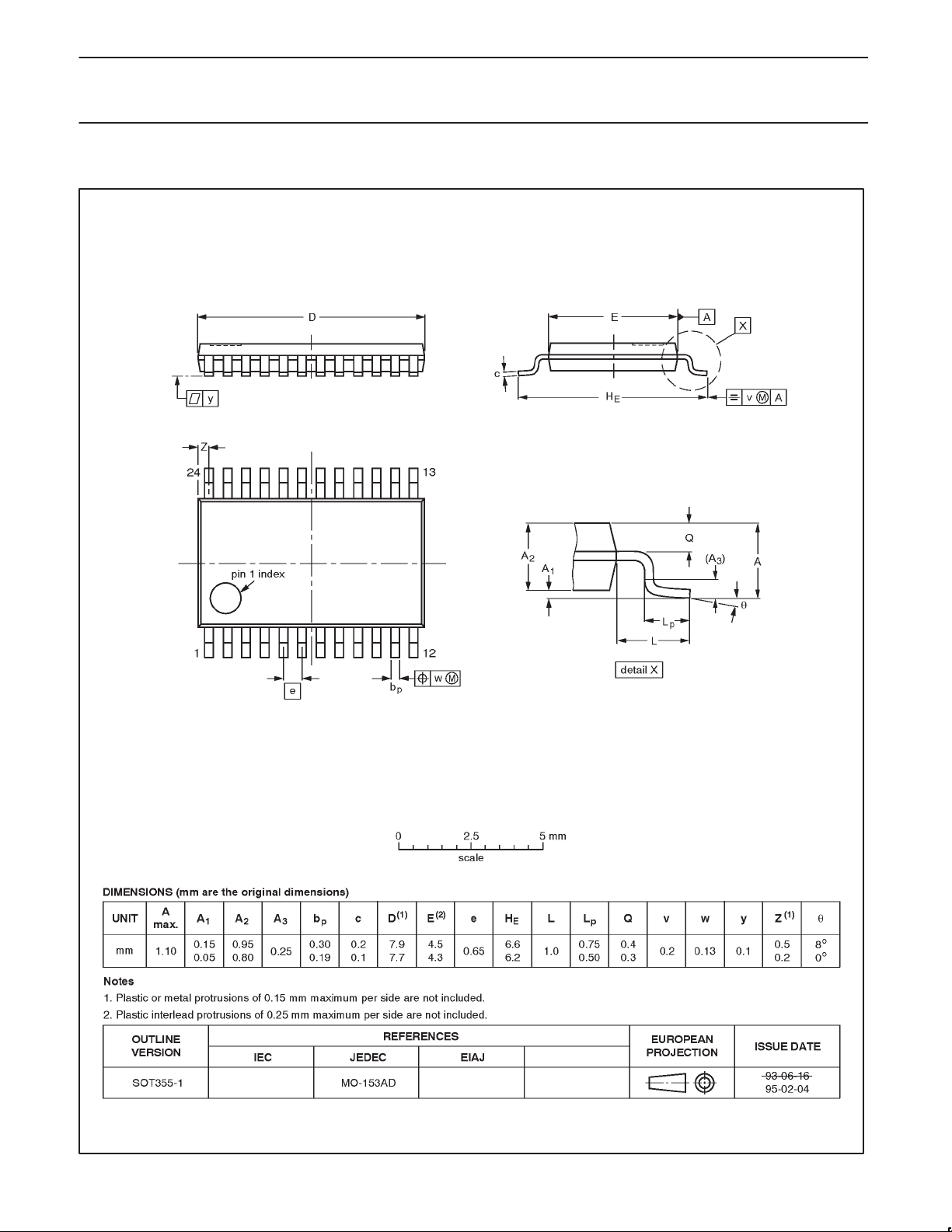
TSSOP24: plastic thin shrink small outline package; 24 leads; body width 4.4 mm SOT355-1
1997 May 23
14
Page 15

Philips Semiconductors Product specification
SA2420Low voltage RF transceiver — 2.45GHz
NOTES
1997 May 23
15
Page 16

Philips Semiconductors Product specification
SA2420Low voltage RF transceiver — 2.45GHz
DEFINITIONS
Data Sheet Identification Product Status Definition
Objective Specification
Preliminary Specification
Product Specification
Formative or in Design
Preproduction Product
Full Production
Philips Semiconductors and Philips Electronics North America Corporation reserve the right to make changes, without notice, in the products,
including circuits, standard cells, and/or software, described or contained herein in order to improve design and/or performance. Philips
Semiconductors assumes no responsibility or liability for the use of any of these products, conveys no license or title under any patent, copyright,
or mask work right to these products, and makes no representations or warranties that these products are free from patent, copyright, or mask
work right infringement, unless otherwise specified. Applications that are described herein for any of these products are for illustrative purposes
only. Philips Semiconductors makes no representation or warranty that such applications will be suitable for the specified use without further testing
or modification.
LIFE SUPPORT APPLICA TIONS
Philips Semiconductors and Philips Electronics North America Corporation Products are not designed for use in life support appliances, devices,
or systems where malfunction of a Philips Semiconductors and Philips Electronics North America Corporation Product can reasonably be expected
to result in a personal injury. Philips Semiconductors and Philips Electronics North America Corporation customers using or selling Philips
Semiconductors and Philips Electronics North America Corporation Products for use in such applications do so at their own risk and agree to fully
indemnify Philips Semiconductors and Philips Electronics North America Corporation for any damages resulting from such improper use or sale.
Philips Semiconductors
811 East Arques Avenue
P.O. Box 3409
Sunnyvale, California 94088–3409
Telephone 800-234-7381
This data sheet contains the design target or goal specifications for product development. Specifications
may change in any manner without notice.
This data sheet contains preliminary data, and supplementary data will be published at a later date. Philips
Semiconductors reserves the right to make changes at any time without notice in order to improve design
and supply the best possible product.
This data sheet contains Final Specifications. Philips Semiconductors reserves the right to make changes
at any time without notice, in order to improve design and supply the best possible product.
Date of release: 05–97
Document order number: 9397 750 03302
1997 May 23
16
 Loading...