

Page 1

INTEGRATED CIRCUITS
SA1920
Dual-band RF front-end
Product specification
Supersedes data of 1998 Apr 07
IC17 Data Handbook
1999 Mar 02
Page 2
Philips Semiconductors Product specification
SA1920Dual-band RF front-end
DESCRIPTION
The SA1920 is an integrated dual-band RF front-end that operates
at both cellular (AMPS, GSM and TDMA) and PCS/DCS (TDMA and
GSM) frequencies, and is designed in a 13 GHz f
BiCMOS
T
process—QUBiC1. The low-band is a combined low-noise amplifier
(LNA) and mixer. The LNA has a 1.7 dB noise figure at 881 MHz
with 17.5 dB of gain and an IIP3 of –5 dBm. The wide-dynamic
range mixer has a 10 dB noise figure at 881 MHz with 9.5 dB of gain
and an IIP3 of +5 dBm.
The high-band contains a receiver front-end, doubler and a high
frequency transmit mixer intended for closed loop transmitters. One
advantage of the high-band architecture is an image-rejection mixer
with over 30 dB of image rejection; thus, eliminating external filter
cost while saving board space. The system noise figure is 4.2 dB at
1960 MHz with a power gain of 23.5 dB and an IIP3 of –12.5 dB.
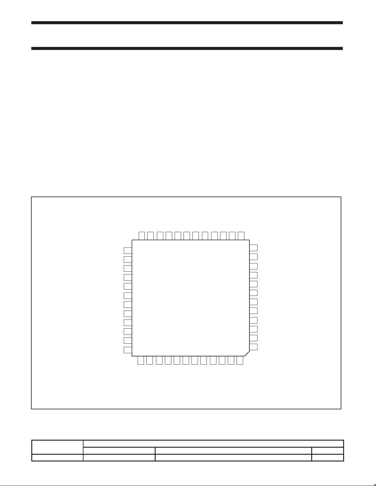
PIN CONFIGURATION
Rx ON
LOW BAND LO A
LOW BAND LO A
HIGH BAND LO B
21222324
25
V
CC
26
Tx ON
27
V
CC
GND
GND
GND
X2 ON
N/C
28
29
30
31
32
33
34
35
36
37 38 39 40 41 42 43
HIGH BAND IMAGE SET I
HIGH BAND LO INPUT
LOW BAND LO INPUT
HIGH BAND IMAGE SET Q
FEATURES
•Low current consumption
•Outstanding low- and high-band noise figure
•Excellent gain stability versus temperature and supply
•Image reject high-band mixer with over 30 dB of rejection
•Increased low-band LNA gain compression during analog
transmission
•LO input and output buffers
•Frequency doubler
•On chip logic for network selection and power down
•Very small outline package
APPLICATIONS
•800 to 1000 MHz analog and digital receivers
•1800 to 2000 MHz digital receivers
•Portable radios
•Digital mobile communications equipment
HIGH BAND LO A
GND
LOW BAND IF B
LOW BAND IF A
HIGH BAND IF B
HIGH BAND IF A
SYN ON
HI/LO
181920
44 45 46 47 48
151617 1314
N/C
12
GND
11
10
Tx B
9
Tx A
GND
8
V
7
CC
GND
6
MIX IN
5
GND
4
Tx IF B
3
Tx IF A
2
N/C
1
N/C
STRONG SIGNAL
GND
CC
GND
V
GND
LOW BAND LNA IN
HIGH BAND LNA IN
LOW BAND LNA OUT
GND
GND
N/C
SR01435
Figure 1. Pin Configuration
ORDERING INFORMATION
TYPE NUMBER
NAME DESCRIPTION VERSION
SA1920 LQFP48 Plastic low profile quad flat package; 48 leads; body 7x7x1.4 mm SOT313-2
1999 Mar 02 853–2057 20918
PACKAGE
2
Page 3

Philips Semiconductors Product specification
SA1920Dual-band RF front-end
PIN DESCRIPTIONS
PIN
NO.
1 N/C No Connection
2 Tx IF A Transmit IF A
3 Tx IF B Transmit IF B
4 GND Ground
5 MIX IN Low Band Mixer Input
6 GND Ground
7 V
8 GND Ground
9 Tx A Transmit Signal A
10 Tx B Transmit Signal B
11 GND Ground
12 N/C No Connection
13 HI/LO High Band/Low Band Control
14 SYN ON LO Buffer Power Control
15 HIGH BAND IF A High Band IF A
16 HIGH BAND IF B High Band IF B
17 LOW BAND IF A Low Band IF A
18 LOW BAND IF B Low Band IF B
19 GND Ground
20 HIGH BAND LO A High Band LO Output
21 HIGH BAND LO B High Band LO Output
22 LOW BAND LO A Low Band LO Output
23 LOW BAND LO B Low Band LO Output
24 Rx ON LNA/Mixer Power Control
25 V
26 Tx ON Tx Mixer/Driver Power
27 V
28 HIGH BAND IMAGE SET I High Band Image Set I
29 GND Ground
30 HIGH BAND LO INPUT High Band LO Connection
31 LOW BAND LO INPUT Low Band LO Connection
32 GND Ground
33 HIGH BAND IMAGE SET Q High Band Image Set Q
34 GND Ground
35 X2 ON Freq. Doubler Power Control
36 N/C No Connection
37 N/C No Connection
38 STRONG SIGNAL Strong Signal Detection
39 GND Ground
40 V
41 GND Ground
42 HIGH BAND LNA IN High Band LNA Input
43 LOW BAND LNA IN Low Band LNA Input
44 GND Ground
45 LOW BAND LNA OUT Low Band LNA Output
46 GND Ground
47 GND Ground
48 N/C No Connection
PIN NAME DESCRIPTION
CC
CC
CC
CC
V
CC
V
CC
V
CC
V
CC
1999 Mar 02
3
Page 4
Philips Semiconductors Product specification
SA1920Dual-band RF front-end
HI/LO
SYN ON
HIGH BAND IF A
HIGH BAND IF B
LOW BAND IF A
LOW BAND IF B
GND
HIGH BAND LO A
HIGH BAND LO B
LOW BAND LO A
LOW BAND LO B
N/C
GND
Tx B
Tx A
REJECT
IMAGE
MIXER
GND
CC
V
X2
GND
MIX IN
GND
Tx IF B
N/C
Tx IF A
N/C
GND
GND
LNA OUT
GND
LOW BAND LNA IN
HIGH BAND LNA IN
GND
V
CC
GND
STRONG SIGNAL
Rx ON
N/C
Tx ON
CC
V
GND
HIGH BAND IMAGE SET I
HIGH BAND LO INPUT
GND
LOW BAND LO INPUT
GND
HIGH BAND IMAGE SET Q
X2 ON
N/C
SR01436
CC
V
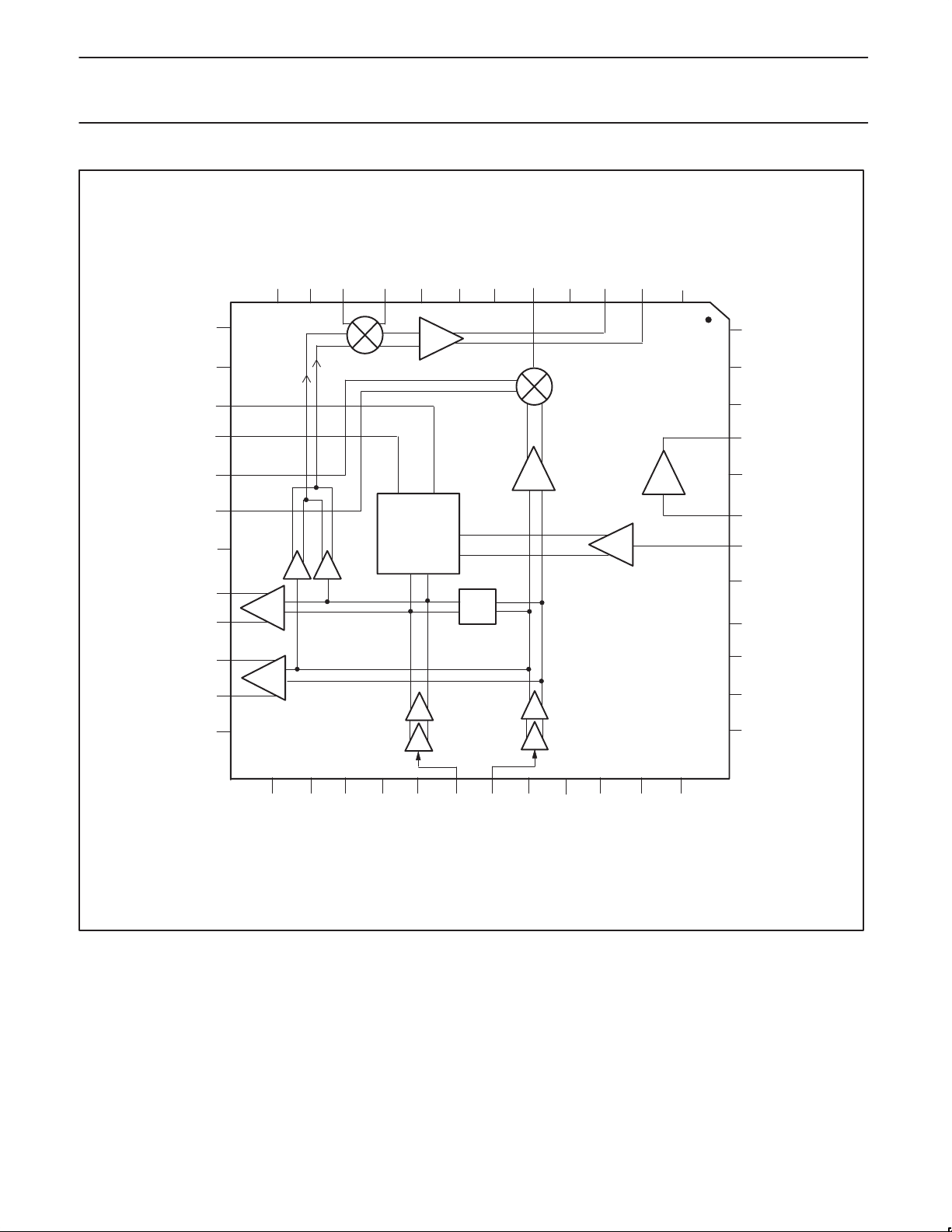
Figure 2. Block Diagram
1999 Mar 02
4
Page 5
Philips Semiconductors Product specification
SA1920Dual-band RF front-end
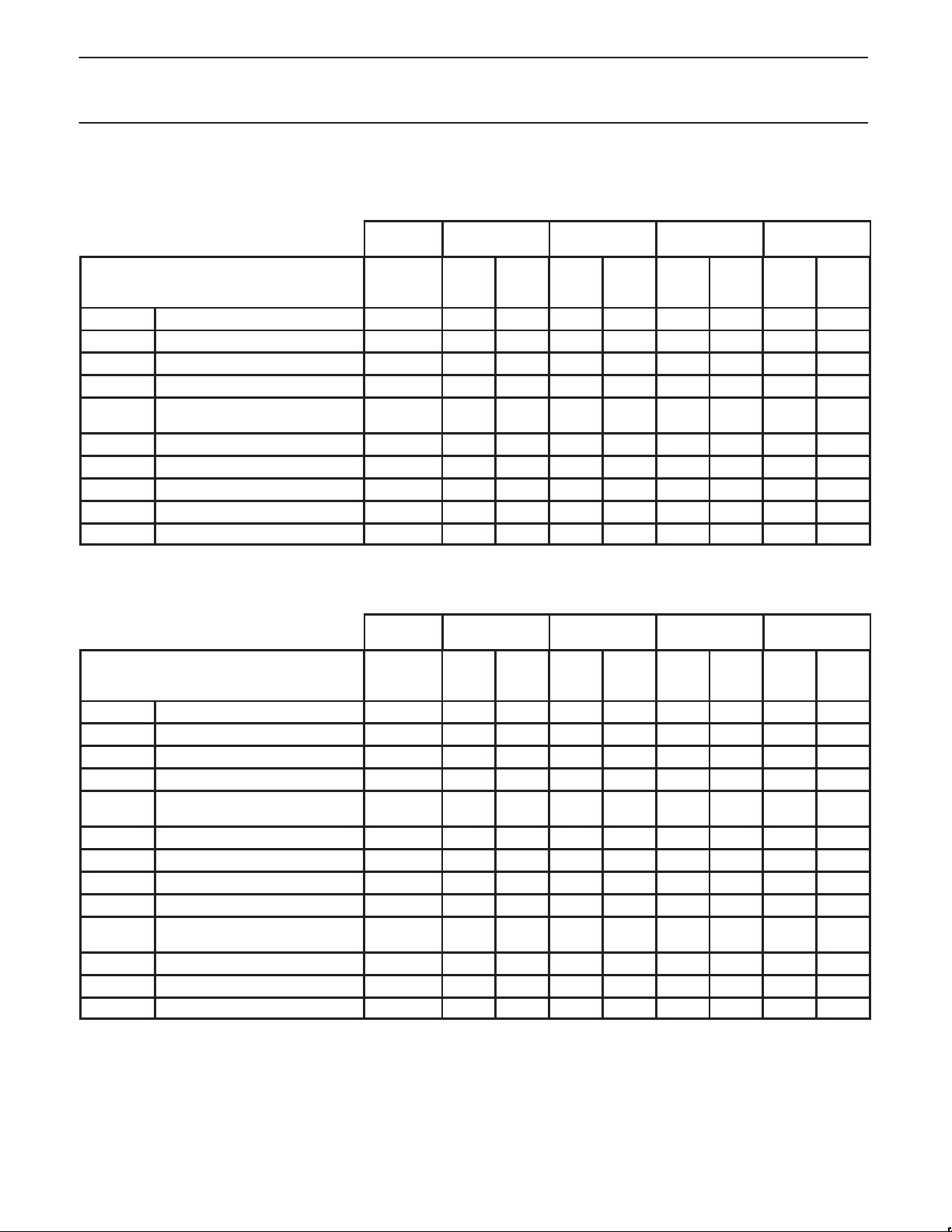
T able 1. POWER DOWN CONTROL
For Applications Not Using a Frequency Doubler, each state is
defined as follows:
DOUBLER
Control State
(Hi/Lo, Syn On, Rx On, Tx On, Strong Signal, X2
ON)
x000xx Sleep Off Off Off Off Off Off Off Off Off
010000 Low-Band LO Buffer on Off Off On Off Off Off Off Off Off
011000 Low-Band Receive Normal Off Off On Off On Off On Off Off
011010 Low-Band receive Strong Signal Off Off On Off Off Off On Off Off
011100 Low-Band Transmit (Analog only) Off Off On Off On
010100 N/A Off Off On Off Off Off Off Off On
110000 High-Band LO Buffer On Off On Off Off Off Off Off Off Off
111000 High-Band Receive Normal Off On Off On Off On Off Off Off
111010 High-Band Receive Strong Signal Off On Off Off Off On Off Off Off
110100 N/A Off On Off Off Off Off Off On Off
LO BUFFER LNA MIXER
High
Band
Low
Band
High
Band
Low
Band
High Bias
High
Band
Off On Off On
Low
Band
TX MIXER
DRIVER
High
Band
Low
Band
For Applications Using a Frequency Doubler, each state is
defined as follows:
DOUBLER
Control State
(Hi/Lo, Syn On, Rx On, Tx On, Strong Signal, X2
ON)
x000xx Sleep Off Off Off Off Off Off Off Off Off
010000 Transmit (Low and High Band) Off Off On Off Off Off Off Off Off
011000 Low-Band Receive Normal Off Off On Off On Off On Off Off
011010 Low-Band Receive Strong Signal Off Off On Off Off Off On Off Off
011110 Low-Band Transmit (Analog only) Off Off On Off On
010100 Low-Band Transmit (GSM) Off Off On Off Off Off Off Off On
010001 Transmit (Low and High Band) On Off On Off Off Off Off Off Off
011001 Low-Band Receive Normal On Off On Off On Off On Off Off
011011 Low-Band Receive Strong Signal On Off On Off Off Off On Off Off
011111 Low-Band Transmit(Analog only) On Off On Off On
111001 High-Band Receive Normal On On On On Off On Off Off Off
111011 High-Band Receive Strong Signal On On On Off Off On Off Off Off
110101 High-Band Transmit (GSM) On On On Off Off Off Off On Off
LO BUFFER LNA MIXER
High
Band
Low
Band
High
Band
Low
Band
High Bias
High Bias
High
Band
Off On Off Off
Off On Off Off
Low
Band
TX MIXER
DRIVER
High
Band
Low
Band
NOTE:
“0” is low logic state; “1” is high logic state.
1999 Mar 02
5
Page 6

Philips Semiconductors Product specification
SA1920Dual-band RF front-end
OPERATION
The low-band contains both an LNA and mixer that is designed to
operate in the 800 to 1000 MHz frequency range. The high-band
contains an LNA and image-rejection mixer that is designed to
operate in the 1800 to 2000 MHz frequency range with over 30 dB of
rejection over an intermediate frequency (IF) range from 100 to
125 MHz.
Image rejection is achieved in the internal architecture by two RF
mixers in quadrature and two all-pass filters in the I and Q IF
channels that phase shift the IF by 45 and 135, respectively. The
two phase shifted IFs are recombined and buffered to produce the
IF output signal.
The LO section consists of an internal all-pass type phase shifter to
provider quadrature LO signals to the receive mixers. The all-pass
filters outputs are buffered before being fed to the receive mixers.
The transmit mixer section consists of a low-noise amplifier, and a
down-convert mixer. In the transmit mode, an internal LO buf fer is
used to drive the transmit IF down-convert mixer.
Low-Band Receive Section
The circuit contains a LNA followed by a wide-band mixer. In a
typical application circuit, the LNA output uses an external pull-up
inductor to VCC and is AC coupled. The mixer IF outputs are
differential. A typical application will load the output buffer with an
inductor across the IF outputs, a pull-up inductor to V
coupled capacitor to the matching network.
and an AC
CC
Low-Band Receive Section (Analog Transmit
Mode)
The bias current of the low-band LNA will increase during analog
transmission, which increases its gain compression point and makes
the receiver less sensitive to PA leakage power for an AMPS
application.
High-Band Receive Section
The circuit contains an LNA followed by two high dynamic range
mixers. These are Gilbert cell mixers; the internal architecture is fully
differential. The LO is shifted in phase by 45 and 135 and mixes
the amplified RF signal to create I and Q channels. The two I and Q
channels are buffered, phase shifted by 45 and 135, respectively ,
amplified and recombined internally to realize the image rejection.
The IF output is differential and of the open-collector type. A typical
application will load the output buffer with an inductor across the IF
outputs, a pull-up inductor to V
the matching network.
and an AC coupled capacitor to
CC
Control Logic Section
Pins HI/LO, SYN ON, Rx On, Tx On, Strong Signal, X2 (doubler)
On, control the logic functions. The HI/LO mode selects between
low-band and high-band operation. The SYN ON mode enables the
LO buffers independent of the other circuitry . When SYN ON is high,
all internal buffers in the LO path of the circuit are turned on, thus
minimizing LO pulling when the remainder of the receive or transmit
chain is powered-up.
The Rx ON mode enables the LO buffers when the device is in the
low-band receive normal, receive strong signal and transmit modes;
the Rx ON mode enables the LO buffers, also, when the device is in
the high-band receive normal, and receive strong signal modes.
The Tx ON mode enables the transmit mixer. The strong signal
mode, when disabled, allows the low- and high-band LNAs to
function normally; and when the strong signal mode is enabled, it
turns-off the low- and high-band LNAs. This is needed when the
input signal is large and needs to be attenuated.
The doubler (X2) on mode enables the doubler. When the doubler is
on, the input signal from the LO buffers is doubled in frequency . The
signal can be used to drive the image-rejection mixer and the output
LO high-band ports. When the doubler mode is on, all other control
logic (see table 1) functions the same.
Local Oscillator (LO) Section
The LO input directly drives the two internal all-pass networks to
provide quadrature LO to the receive mixers. A synthesizer-on (SYN
ON) mode is used to power-up all LO input buffers, thus minimizing
the pulling effect on the external VCO when entering receive or
transmit mode.
Transmit Mixer Section
The transmit mixer is used for down-conversion to the transmit IF. Its
inputs are coupled to the transmit RF which is down-converted to a
modulated transmit IF frequency , and phase-locked with the
baseband modulation.
The IF outputs are HIGH impedance (open-collector type). A typical
application will load the output buffer with an inductor across the IF
outputs, a pull-up inductor to V
matching network.
and AC coupled capacitors to the
CC
1999 Mar 02
6
Page 7

Philips Semiconductors Product specification
SA1920Dual-band RF front-end
ABSOLUTE MAXIMUM RATINGS
QUANTITY SYMBOL VALUE UNIT
Input supply voltage at pins: 7, 25, 27, 40 V
Power dissipation P
Input power at all ports P
Operating temperature range (pin temp) T
Storage temperature range T
CC
D
IN
O
srg
DC ELECTRICAL CHARACTERISTICS
Unless otherwise specified, all Input/Output ports are single-ended.
DC PARAMETERS
V
= +3.75 V, T
CC
DC Supply voltage V
Current Consumption: Sleep Mode X000XX I
Low Band Receive Normal 011000 I
Low Band Receive Strong 011010 I
Low Band Transmit (Analog) 011110 I
Low Band Transmit (GSM) 010100 I
High Band Receive Normal 111000 I
High Band Receive Strong 111010 I
High Band Transmit (GSM) 110100 I
Frequency Doubler 8.8 mA
Logic Low Input 0 0.5 V
Logic High Input 1.9 4.0 V
= –40 to +85°C unless otherwise noted
A
QUANTITY
CONDITION SYMBOL MIN. TYP. MAX. UNIT
CC
CC
CC
CC
CC
CC
CC
CC
CC
3.6 3.75 3.9 V
10.1 12.5 15.2 mA
35.0 42.0 53.0 mA
4.75 V
150 mW
+20 dBm
–40 to+85 °C
–65 to +125 °C
1 100
A
8.8 mA
18.0 mA
16.0 mA
38.0 mA
21.5 mA
1999 Mar 02
7
Page 8
Philips Semiconductors Product specification
SA1920Dual-band RF front-end
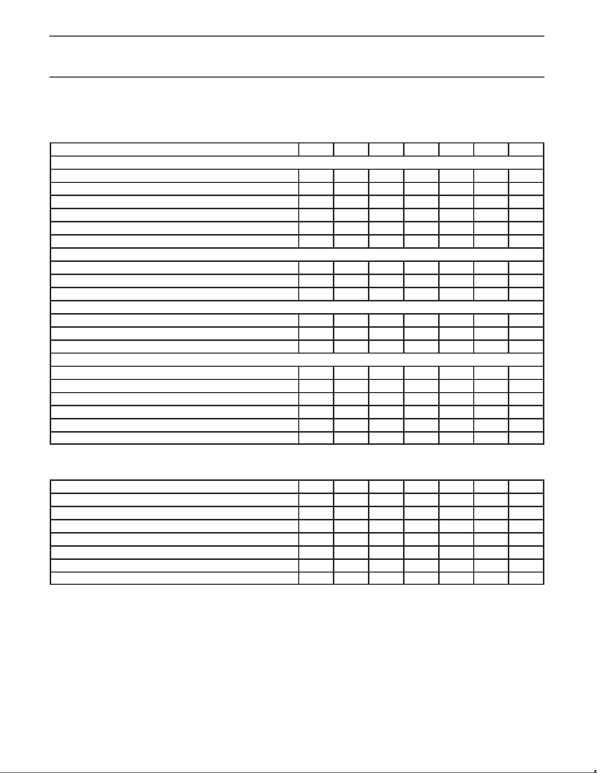
AC ELECTRICAL CHARACTERISTICS
Low-Band, Dual Mode of Operation
VCC = +3.75 V, FreqRF = 881 MHz, FreqLO = 991.52 MHz, Pin = –3 dBm, TA = +25C; unless otherwise stated
PARAMETERS
System
RF Input Frequency Range 869 881 960 MHz
IF Frequency 110.52 MHz
LO Frequency 991.52 MHz
Cascaded Power Gain; includes 3dB filter loss 22.5 24 25.5 dB
Power Gain Reduction (Strong Signal Mode—LNA Off) 29 35 41 dB
Cascaded Noise Figure; includes 3dB filter loss 2.6 dB
LNA
LNA Gain 17 17.5 18 dB
LNA IIP3 –6 –5 –4 dBm
LNA Noise Figure 1.6 1.7 1.8 dB
Mixer
Mixer Gain 9 9.5 10 dB
Mixer IIP3 4 5 6 dBm
Mixer Noise Figure 9 10 11 dB
Other
Input Impedance, RF Port 50
Return Loss at LNA Inputs and Output –10 dB 1
Return Loss at Mixer Input and Outputs –10 dB 1
LO leakage at RF Port –42 dBm
LO Input Power –5 –3 –1 dBm
Turn ON/OFF Time 100
Min
–3
TYP
+3
Max UNITS NOTES
W
msec
Low-Band LO Buffer
PARAMETERS Min
LO Frequency 991.52 MHz
Differential Output Power –7 dBm
Differential Output Impedance 100
Harmonic Content –20 dBc
Input Power –5 –3 –1 dBm
Input Impedance 50
Turn On/Off T ime 30
1999 Mar 02
8
–3
TYP.
+3
Max UNITS NOTES
msec
W
W
1
Page 9
Philips Semiconductors Product specification
50 dBm IN Referred to RF In ut Port
SA1920Dual-band RF front-end
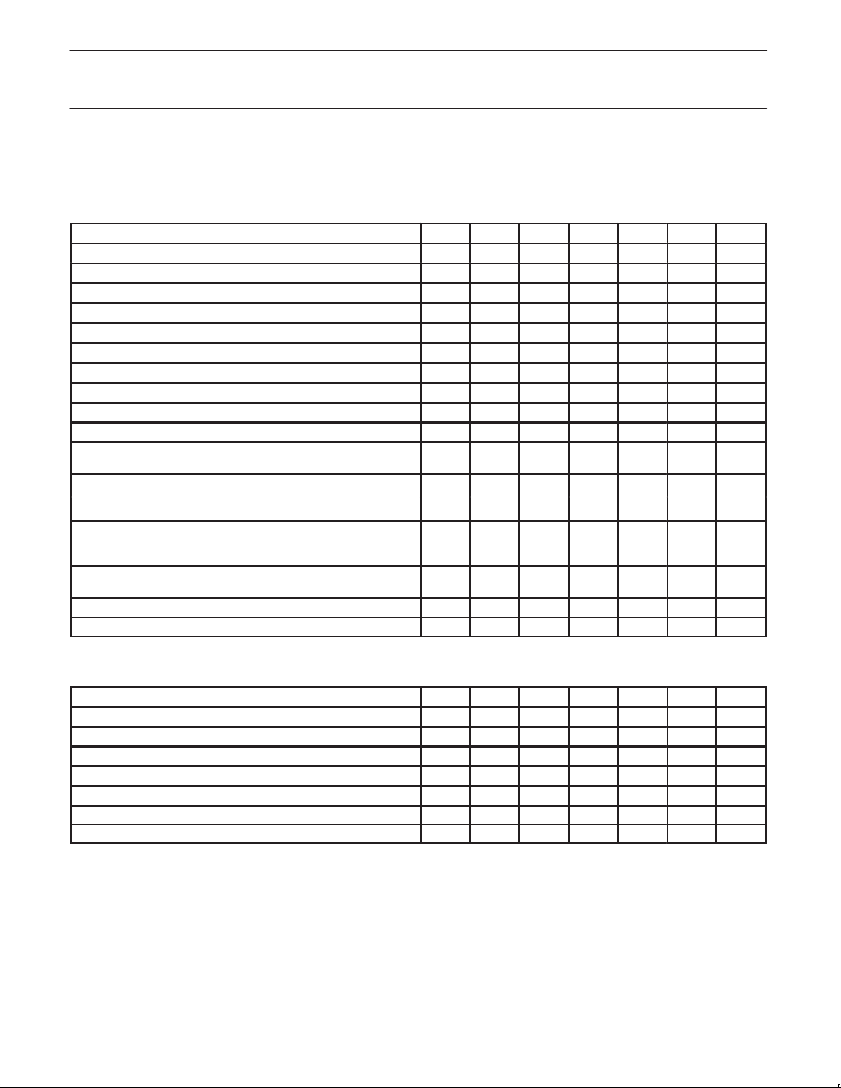
AC ELECTRICAL CHARACTERISTICS
High-Band, Single Mode of Operation
LNA and Image Reject Mixer
VCC = +3.75 V, FreqRF = 1960 MHz, FreqLO = 2070.52 MHz, Pin = –3 dBm, TA = +25C; unless otherwise stated
PARAMETERS
RF Input Frequency Range 1805 1990 MHz
IF Frequency 100 110.52 125 MHz
LO Frequency 1905 2115 MHz
Power Gain 21 23.5 25 dB
Power Gain Reduction (Strong Signal Mode—LNA Off) 40 47 54 dB
Noise Figure 4.0 4.2 4.4 dB
Input Impedance, RF Port 50
Return Loss at Inputs –10 dB 1
LO leakage at RF Port –48 dBm
1 dB RF Input Compression Point –24 dBm
IP3 (3RD Order Intermodulation Product)
Referred to the RF Input Port
(2 x LO) – (2 x RF) Spur Performance
–
Measure at LO = 2040 MHz and RF = 1985 MHz
(3 x LO) – (3 x RF) Spur Performance.
–50 dBm IN Referred to RF Input Port.
Measure at LO = 2040 MHz and RF = 2003 MHz.
Image rejection, fRX+2fIF or f
Referred to the RF Input Port
LO Input Power –5 –3 –1 dBm
Turn ON/OFF Time 30
RX
p
–2f
IF
MIN
30 35 dB
–3
–15 –12.5 –10 dBm
TYP.
–65 dBc
–62.5 dBc
+3
MAX UNITS NOTES
msec
W
High-Band LO Buffer
LO Frequency Range 1905 2115 MHz
Differential Output Power –9 dBm
Differential Output Impedance 100
Harmonic Content –20 dBc
Input Power –5 –3 –1 dBm
Input Impedance 50
Turn On/Off T ime 30
1999 Mar 02
PARAMETERS MIN
9
–3
TYP.
+3
MAX UNITS NOTES
W
W
msec
1
Page 10

Philips Semiconductors Product specification
SA1920Dual-band RF front-end
Frequency Doubler
PARAMETERS MIN
Output Frequency Range 1905 2115 MHz
Output Power –9 dBm
Differential Output Impedance 100
Harmonic Content (3F, 4F , etc.) –20 dBc
Subharmonic Content (Fi) –20 dBc
Non-Harmonic Content 80 dBc
Turn On/Off T ime 30
Phase Noise Degradation, ∆ f = 30kHz 6 dB
–3
Transmit Mixer
PARAMETERS MIN
TX Mixer Input Frequency 824 1910 MHz
TX RF Input Impedance, Balanced 200
TX Mixer Output Frequency 70 200 MHz
TX IF Load Impedance 1000
Maximum TX IF Load Capacitance 2 pF
Conversion Power Gain 15 16 17 dB 2
1 dB Input Compression Point –17 dBm
IIP2 20 dBm
IIP3 –9 –7 –5 dBm
Noise Figure (double sideband) 7.5 dB
Reverse Isolation T
Isolation LOIN–T
NOTES:
1. External matching network is required.
2. From 200W input to a 1kW output.
XIN
XIN
–LO
IN
40 dB
40 dB
–3
TYP.
TYP.
+3
+3
MAX UNITS NOTES
W
msec
MAX UNITS NOTES
W
W
1999 Mar 02
10
Page 11
Philips Semiconductors Product specification
SA1920Dual-band RF front-end
P7
B
R15
J24–4
AP36
3.92K
A
Maletxsma
4763–000–00
I1695
6
U1
SUM PORT
LRPS–2–11
PORT 2
PORT 1
3
4
3
AT5
PAT–3
1
R21
51.1
10 pf
C25
C26
J22–5
J21–2
J100–4
J100–2
J100–3
J100–5
J23–4
AP39
AP11
DPS1LF
3
R14
PAT–3
10 pf
R20
51.1
3.92K
R12
1
AT6
1
DPS1HF
DPS1LS
DPS1HS
C32
L4
1 uH
BA
C12
C16
0.1 uf
1000 pf
100 pf
DP19
C13
1000 pf
DO NOT ASSEMBLE
1
R28
J1–3
AP43
3.92K
C8
L12
3.3 pf
DPS1
C38
1000 pf
C37
100 pf
4.7 nH
R27
J28–2
J29–2
J28–3
P8
3.92K
AP16
R31
3.92K
C22
A
AT7
13
AP47
332
R29
A
C30
B
PAT–3
R22
L9
33 pf
1.5 pf
Maleltxsma
4763–000–00
I1696
51.1
8.2 nH
B
R30
J26–3
AP16
3.92K
P6
B
A
Maleltxsma
4763–000–00
I1693
AT8
PAT–3
13
R19
51.1
L8
8.2 nH
A
B
C21
33 pf
C29
2.2 pf
DPS1
C33
0.1 uf
L5
1 uH
BA
C14
1000 pf
C17
100 pf
DP31
J25–2
DP23
J26–2
AP14
R16
1
R1
AP45
DUT–48
N/C
N/C
DUT–1
L2
A
C23
3.92K
J1–4
330 nH
8.2 pf
DUT–45
DUT–46
LBLOUT
RxMxGND
SA1920
TXIFA
TXIFB
DUT–2
DUT–3
coil
B
C24
13
AT9
A
B
P1
DUT–47
GND
10 pf
R32
PAT–10
Maleltxsma
DUT–44
DUT–41
GND
GND
GND
GND
DUT–4
DUT–6
R2
562
L1
A
C9
5.6 pf
1
I1688
4763–000–00
330 nH
B
C1
DUT–43
LBLIN
LBMIN
DUT–5
1000 pf
DPS1
DUT–42
HBLIN
GND
GND
VCC
DUT–7
DUT–8
DUT–11
C15
100 pf
C10
1000 pf
B
L3
1 uH
A
C31
0.1 uf
1K
R13
AP9
J2–4
N/C
DUT–12
TXA
DUT–9
C18
R3
AP10
J2–5
DUT–40
VCC
TXB
DUT–10
33 pf
33 pf
C19
C2
1.5 pf
3.92K
R17
AT10
PA T–3
13
A
B
P2
DUT–39
GND
51.1
R4
I1689
4763–000–00
Maleltxsma
DUT–38
STRONG
3.92K
AP42
J6–5
DUT–37
N/C
HILO
DUT–13
DP33
J13–2
DUT–36
N/C
HBIFA
SYNON
DUT–14
DUT–15
C5
13
A
P3
DP34
J13–3
DUT–35
X2ON
C3
A
8.2 pf
R10
AT1
PA T–10
B
DUT–34
GND
IMAGE
REJECT
MIXER
5.6 pf
L6
330 nH
B
A
1
MaleLTXAC_SMA
4763–000–00
L10
R9
I1929
HBIFB
DUT–16
330 nH
1.21K
DUT–33
LBBPS
C27
5.6 pf
C4
B
DPS1
R26
AP46
1000 pf
3.92K
J11–2
DUT–32
DUT–31
GND
LBTNK
LBIFA
DUT–17
C7
8.2 pf
L7
A
A
C6
5.6 pf
1
R18
AT2
PA T–10
13
A
B
P5
Maleltxsma
LBIFB
DUT–18
C28
4.7 pf
330 nH
B
L11
330 nH
B
R11
4.32K
DPS1
4763–000–00
I1692
C11
DUT–30
HBTNK
1000 pf
R25
AP44
J12–4
U2
3.92K
DUT–29
DUT–28
DUT–27
DUT–26
DUT–25
GND
1
R24
1
1
AT4
AT3
PAT–10
3
3
3
4
PORT 1
PORT 2
SUM PORT
LRPS–2–11
6
A
B
P4
Maletxsma
4763–000–00
VCC
HBBPS
2X
HBLOA
HBLOB
GND
DUT–19
DUT–20
DUT–21
C34
33 pf
1
R23
PAT–10
C20
33 pf
R8
3.92KR73.92KR53.92K
I1691
AP41
AP40
J11–5
J15–3
C36
33 pf
R6
AP38
TXON
LBLOA
DUT–22
C35
33 pf
3.92K
J20–3
LBLOB
DUT–23
AP12
J21–3
VCC
RXON
DUT–24
DP26
J16–2
SR01801
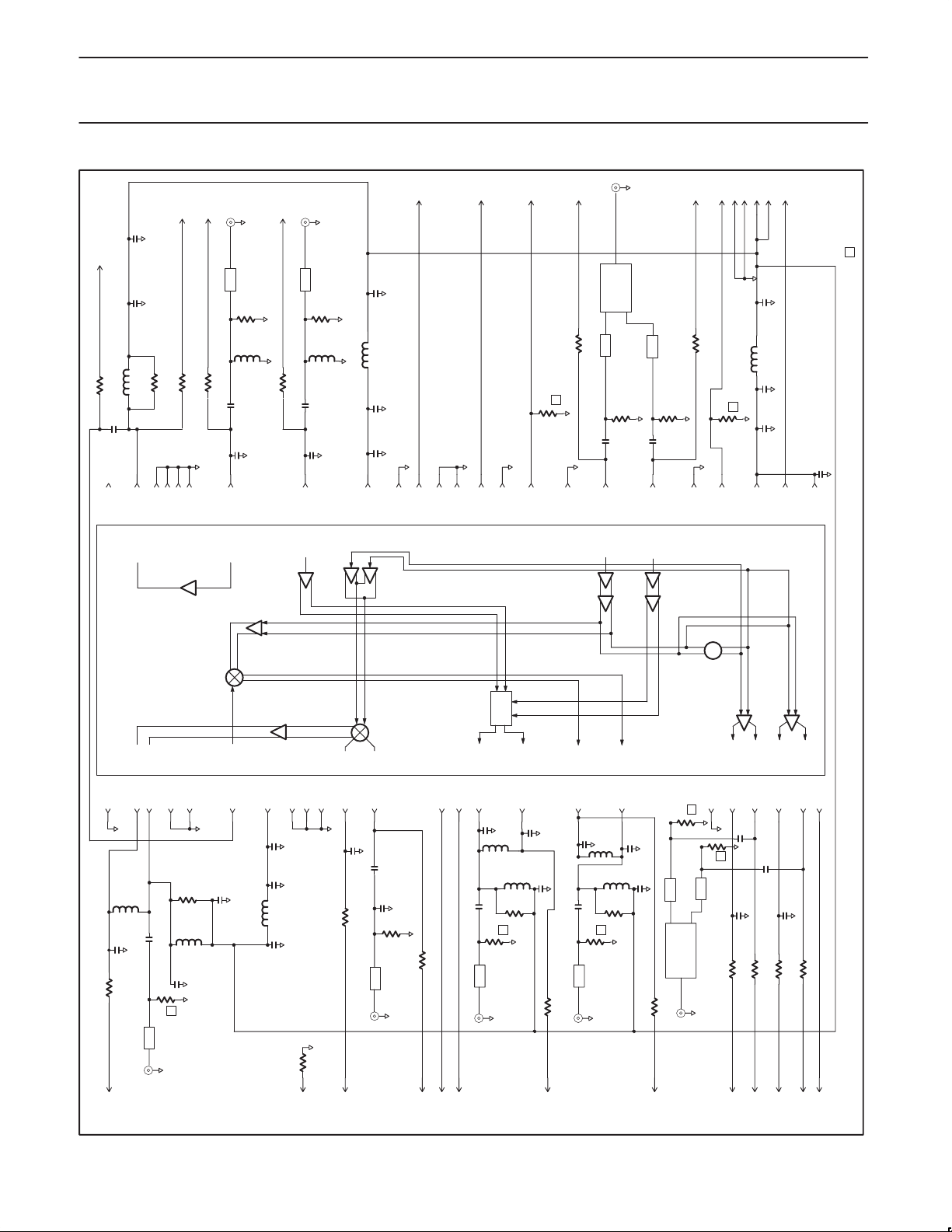
Figure 3. SA1920 Dual-Band Test Circuit
1999 Mar 02
11
Page 12
Philips Semiconductors Product specification
SA1920Dual-band RF front-end
J19
SMA
LBLOIN
J20
SMA
C35
J16
J17
1.5 pF
SMA
HBLIN
SMA
LBLIN
C20
33 pF
L5
C27
C24
C18
33 pF
6.8 nH
100 nF
47 pF
C34
10 nF
J6
STRONG
N/C
STRONG
GND
VCC
GND
HBLIN
LBLIN
GND
LBLOUT
GND
GND
N/C
J5
NOTE: LOGIC PIN MARKED
X2 ON APPLICATION DEMO
BOARD SHOULD BE SET
TO 0 (GND) FOR CORRECT
OPERATION
N/C
X2ON
36
35
37
38
39
40
41
42
43
44
45
46
47
48
X2ON
GND
34
QSET
33
HBLOIN
C31
REJECT
MIXER
GND
29
UL
ISET
28
R4
2.2 K
C15 10 pF
C14 10 pF
HBLOIN
LBLOIN
GND
32
31
30
IMAGE
VCC
27
TXON
26
J4
TXON
5 pF
47 pFC16
VCC
25
24
23
22
21
20
19
5 pF
18
17
16
15
14
13
100 nFC26
RXON
LBLOB
LBLOA
HBLOB
HBLOA
GND
LBIFB
LBIFA
HBIFB
HBIFA
SYNON
HILO
J3
RXON
J9
C6 33 pF
L3
220 nH
SMA
LBLOBJ7SMA
L10
UL
C7 33 pF
C10
C11
C12
3.3 pF
C13
LBLOAJ8SMA
L11
UL
UL
L4
270 nH
UL
HBLOB
J10
SMA
HBLOA
UL
C8 33 pF
C9 33 pF
LBMOUT
HBMOUT
J15
SMA
LBLOUT
1999 Mar 02
1
2
3
4
5
6
7
8
9
10
11
12
C30
L7
220 nH
SR01813
3.9 pF
C29
C28
L8
R2
6.8 pF
6.8 pF
150 nH
2K
VCC
GND
C34
33 pF
C19
1 pF
R3
620
L9
8.2 nH
C32
U1
SA1920
10 nF
(JEANNE)
6.8 pFC3
L6 8.2 nH
J1
SMA
GND
LBMIN
CC
V
GND
C22 47 pF
TXA
C4 33 pF
C25 100 nF
N/C
L1
10 pFC1
180 nH
8.2 pFC2
TXIFB
TXIFA
3.9 pFC21
J18
SMA
MGND1
2KR1
TXOUT
C17
LBMIN
180 nHL2
100 nF
J2
TXB
C5 33 pF
SMA
TXIN
GND
C23 1.5 pF
N/C
J11
HILO
J12
SYNON
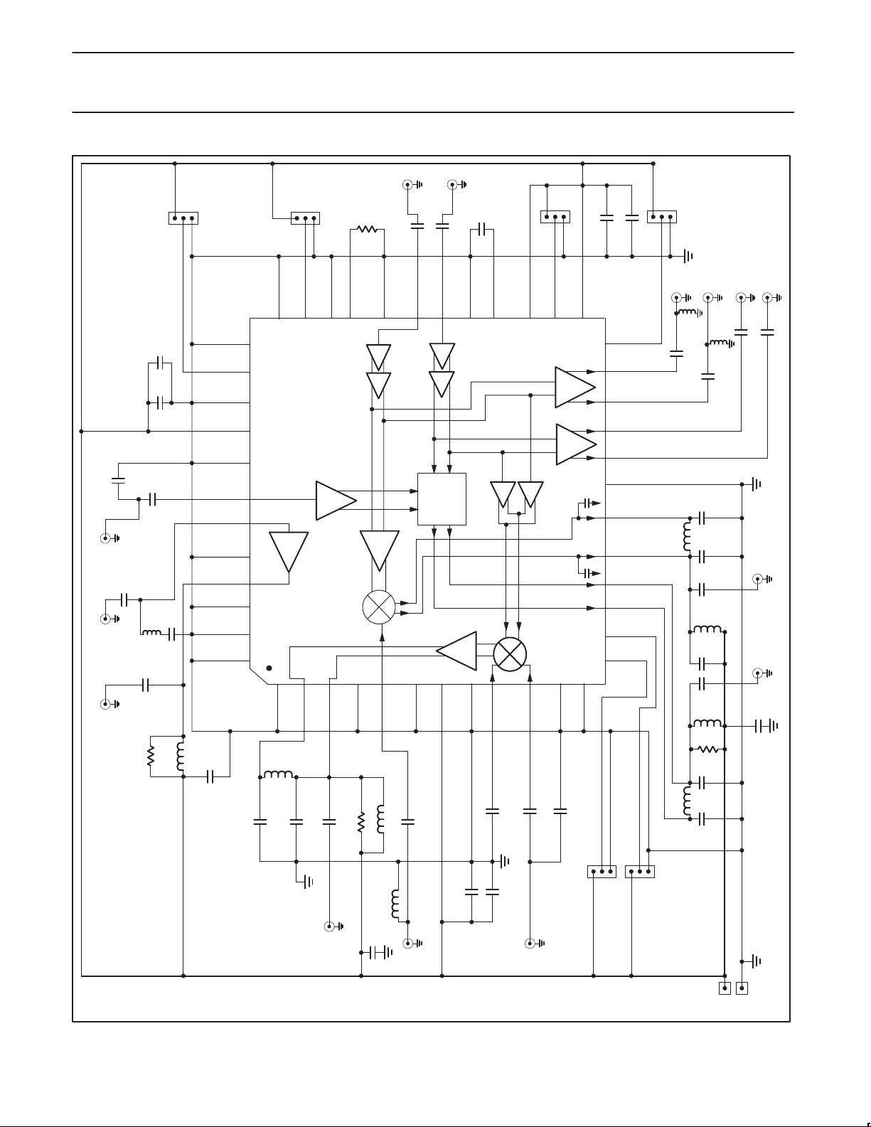
Figure 4. SA1920 Dual-Band Application Circuit
12
Page 13
Philips Semiconductors Product specification
SA1920Dual-band RF front-end
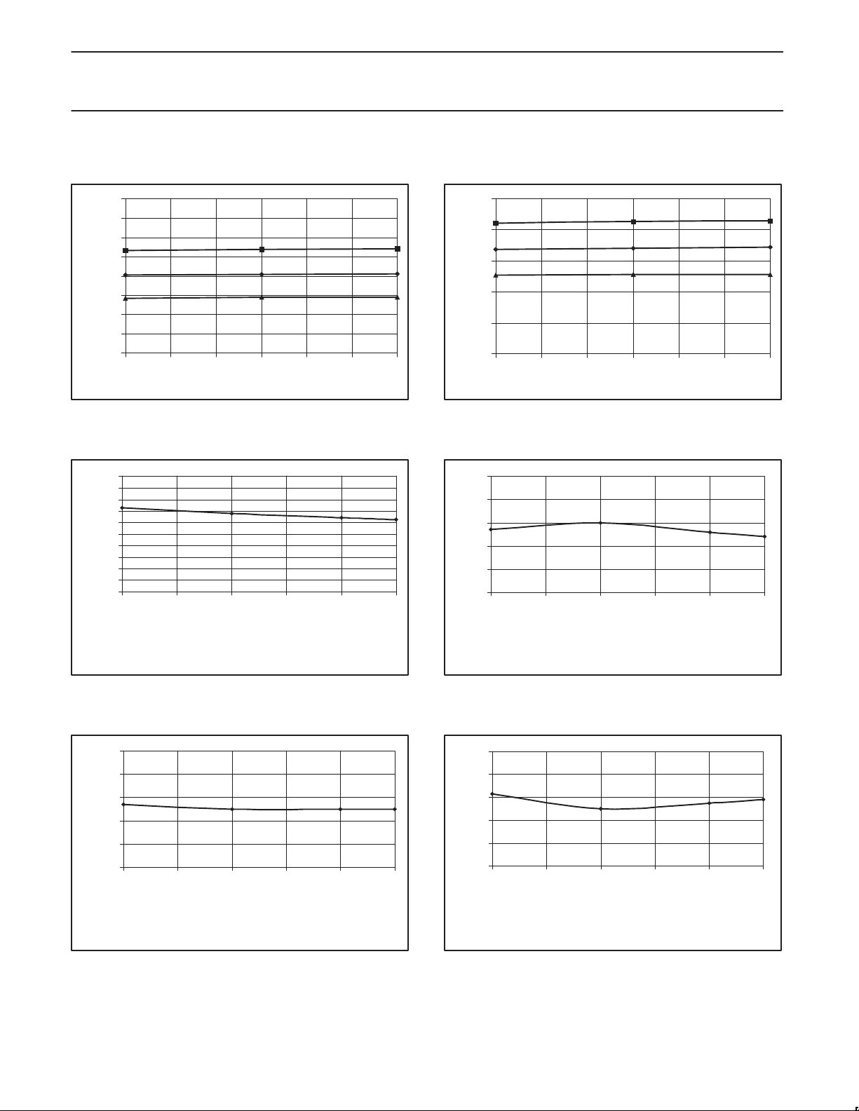
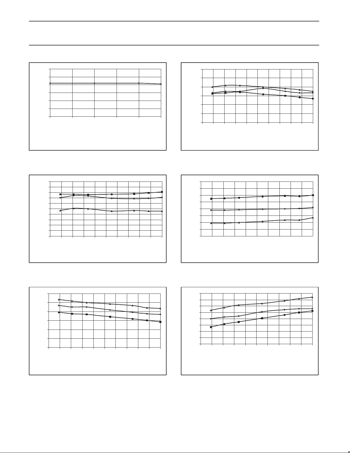
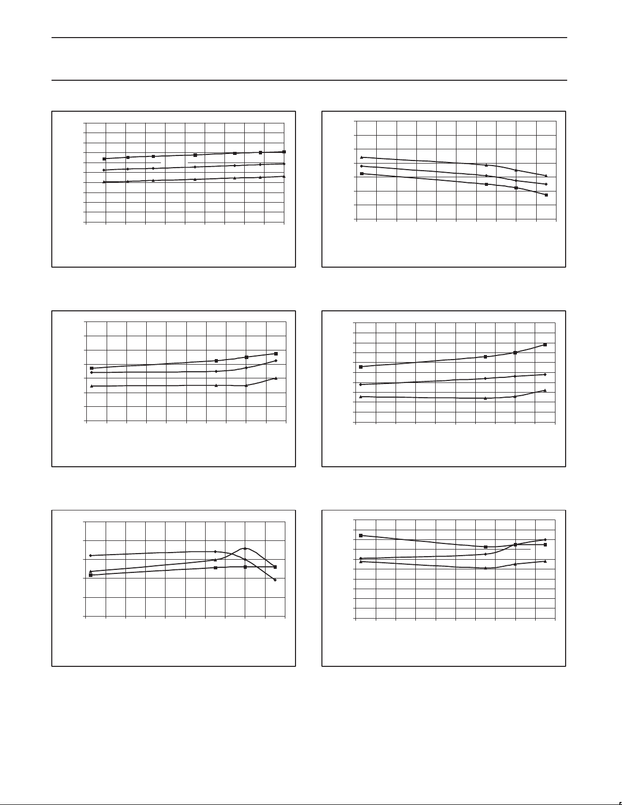
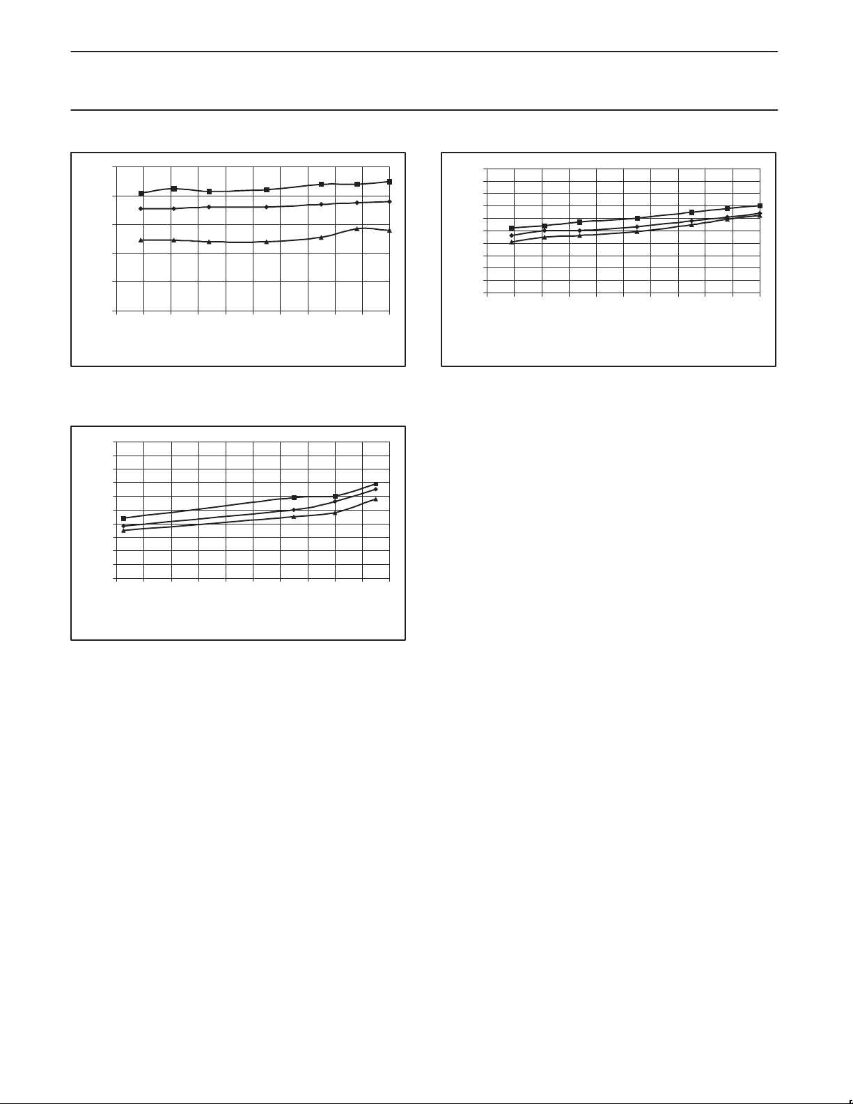
PERFORMANCE CHARACTERISTICS
VCC = +3.75 V, FreqRF = 1960 MHz, FreqLO = 2070.52 MHz, Pin = –5 dBm, TA = +25C; unless otherwise stated
16.0
15.0
14.0
13.0
I
CC
(mA)
12.0
11.0
10.0
9.0
8.0
3.60 3.70 3.80 3.90
3.65 3.75 3.85
+85°C
+25°C
–40°C
V
(V)
CC
SR01613
50.0
+85°C
45.0
40.0
I
CC
(mA)
35.0
30.0
25.0
3.60 3.70 3.80 3.90
3.65 3.75 3.85
+25°C
–40°C
VCC (V)
SR01614
Figure 5. Low Band Receive Normal I
30
28
26
24
22
GAIN
20
(dB)
18
16
14
12
10
100 105 110 115 120 125
IF FREQUENCY (MHz)
Figure 7. High Band Gain vs. IF Frequency
–10
–11
–12
IP3
(dBm)
–13
–14
–15
100 105 110 115 120 125
IF FREQUENCY (MHz)
CC
SR01610
Figure 6. High Band Receive Normal I
45
40
35
30
REJECTION (dB)
25
20
100 105 110 115 120 125
IF FREQUENCY (MHz)
CC
Figure 8. High Band Image Rejection vs. IF Frequency
20
18
16
IP2
(dBm)
14
12
10
100 105 110 115 120 125
IF FREQUENCY (MHz)
SR01609
1999 Mar 02
Figure 9. High Band IP3 vs. IF Frequency
SR01631
SR01611
Figure 10. High Band IP2 vs. IF Frequency
13
Page 14
Philips Semiconductors Product specification
SA1920Dual-band RF front-end
6.0
5.0
4.0
3.0
2.0
1.0
NOISE FIGURE (dBm)
0.0
100 105 110 115 120 125
IF FREQUENCY (MHz)
Figure 11. High Band NF vs. IF Frequency
–2
–3
–4
–5
–6
IP3
–7
(dBm)
–8
–9
–10
–11
–12
860 880 900 920 940 960
870 890 910 930 950
–40°C
FREQUENCY (MHz)
+85°C
+25°C
SR01612
20
19
18
GAIN
(dB)
17
16
15
14
860 880 900 920 940 960
+25°C
870 890 910 930 950
–40°C
+85°C
FREQUENCY (MHz)
Figure 12. LB LNA Gain vs. Frequency
2.6
2.4
2.2
2
1.8
1.6
1.4
NOISE FIGURE (dB)
1.2
1
860 880 900 920 940 960
870 890 910 930 950
+85°C
+25°C
–40°C
FREQUNCY (MHz)
SR01615
Figure 13. LB LNA IP3 vs. Frequency
12
10
8
GAIN
(dB)
6
4
2
0
870 890 910 930 950
860 880 900 920 940 960
–40°C
+25°C
+85°C
FREQUENCY (MHz)
Figure 15. LB Mixer Gain vs. Frequency
SR01616
SR01618
Figure 14. LB LNA Noise Figure vs. Frequency
8
7
6
5
IP3
(dBm)
4
3
2
1
0
860 880 900 920 940 960
–40°C
+25°C
+85°C
FREQUENCY (MHz)
Figure 16. LB Mixer IP3 vs. Frequency
SR01617
950930910890870
SR01619
1999 Mar 02
14
Page 15
Philips Semiconductors Product specification
SA1920Dual-band RF front-end
15
14
13
12
11
10
9
8
NOISE FIGURE (dB)
7
6
5
870 890 910 930 950
860 880 900 920 940 960
+25°C
–40°C
FREQUENCY (MHz)
+85°C
Figure 17. LB Mixer Noise Figure vs. Frequency
–6
–8
–10
–12
IP3
(dBm)
–14
–16
–18
–20
1800 1900 2000
1880186018401820 1920 1940 1960 1980
FREQUENCY (MHz)
+85°C
+25°C
–40°C
SR01620
32
30
28
26
GAIN
(dB)
24
22
20
18
1800 1900 2000
–40°C
+25°C
+85°C
FREQUENCY (MHz)
Figure 18. HB Gain vs. Frequency
7
6.5
6
5.5
5
4.5
4
3.5
NOISE FIGURE (dB)
3
2.5
2
1800 1900 2000
+85°C
+25°C
–40°C
1880186018401820 1920 1940 1960 1980
FREQUENCY (MHz)
19801960194019201880186018401820
SR01621
SR01622
Figure 19. HB IP3 vs. Frequency
45
40
35
30
25
IMAGE REJECTION (dB)
20
+25°C
–40°C
+85°C
1800 1900 2000
1880186018401820 1920 1940 1960 1980
FREQUENCY (MHz)
SR01624
Figure 21. HB Image Rejection vs. Frequency
Figure 20. HB Noise Figure vs. Frequency
20
18
16
14
12
IP2
10
(dBm)
8
6
4
2
0
1800 1900 2000
+25°C
1880186018401820 1920 1940 1960 1980
FREQUENCY (MHz)
+85°C
–40°C
Figure 22. HB IP2 vs. Frequency
SR01623
+25°C
+85°C
SR01625
1999 Mar 02
15
Page 16
Philips Semiconductors Product specification
SA1920Dual-band RF front-end
–15
–17
–19
–21
1 dB COMP (dBm)
–23
–25
860 870 880 890 900 910 920 930 940 950 960
+85°C
+25°C
–40°C
FREQUENCY (MHz)
SR01628
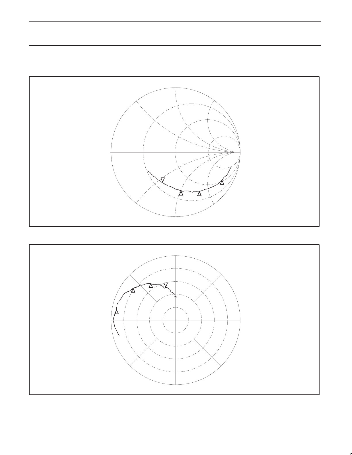
Figure 23. LB LNA 1 dB Compression vs. Frequency
–20
–21
–22
–23
–24
–25
–26
–27
1 dB COMP (dBm)
–28
–29
–30
1800 1900 20001920 1940 1960 19801880186018401820
+85°C
FREQUENCY (MHz)
+25°C
–40°C
–10
–11
–12
–13
–14
–15
–16
–17
1 dB COMP (dBm)
–18
–19
–20
860 870 880 890 900 910 920 930 940 950 960
+85°C
+25°C
–40°C
FREQUENCY (MHz)
SR01629
Figure 24. LB Mixer 1 dB Compression vs. Frequency
SR01630
Figure 25. HB 1 dB Compression vs. Frequency
1999 Mar 02
16
Page 17
Philips Semiconductors Product specification
SA1920Dual-band RF front-end
S-PARAMETERS
1: 56.906Ω
–165.14Ω
200MHz
2: 32.531Ω
–80.145Ω
400MHz
3: 27.213Ω
–50.76Ω
600MHz
4: 22.594Ω
–28.63Ω
6.1759pF
900.125MHz
4
1
START: 100MHz
STOP: 1.35GHz
3
2
SR01632
Figure 26. Typical S11 of the Low Band LNA at 3.75 V for the Low Band Receive Normal Mode
1: 9.2256U
170.16°
200MHz
2: 8.1698U
4
3
2
1
142.74°
400MHz
3: 6.7943U
124.27°
600MHz
4: 5.2793U
106.87°
900MHz
1999 Mar 02
START: 100MHz
STOP: 1.35GHz
SR01643
Figure 27. Typical S21 of the Low Band LNA @ 3.75V for the Low Band Receive Normal Mode
17
Page 18
Philips Semiconductors Product specification
SA1920Dual-band RF front-end
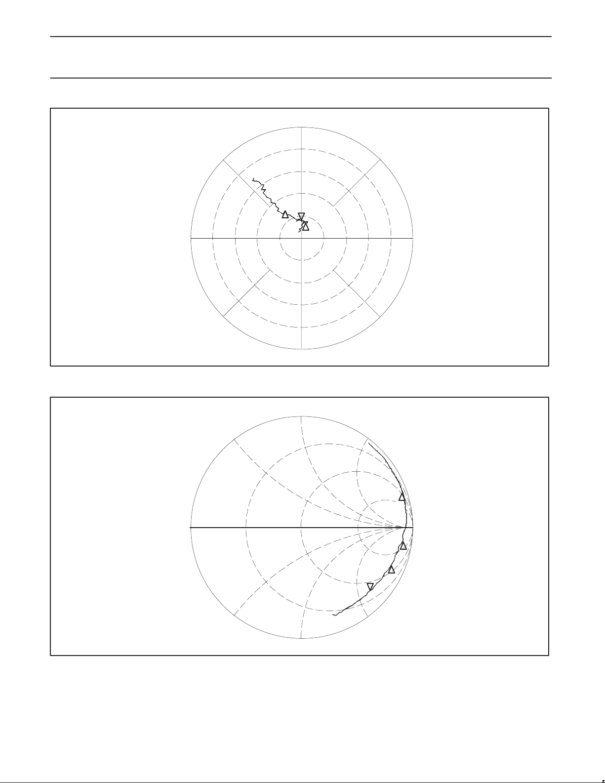
2: 7.0159mU
75.611°
400MHz
3: 7.8297mU
90.185°
600MHz
4: 14.215mU
120.84°
900MHz
3
4
2
START: 100MHz
STOP: 1.35GHz
SR01644
Figure 28. Typical S12 of the Low Band LNA @ 3.75V for the Low Band Receive Normal Mode
1: 35.5Ω
294.66Ω
200MHz
2: 351.72Ω
–537.09Ω
400MHz
3: 77.625Ω
–220.38Ω
600MHz
4: 30.91Ω
–120.37Ω
1
1.4692pF
900MHz
2
3
4
1999 Mar 02
START: 100MHz
STOP: 1.35GHz
SR01633
Figure 29. Typical S22 of the Low Band LNA @ 3.75V for the Low Band Receive Normal Mode
18
Page 19
Philips Semiconductors Product specification
SA1920Dual-band RF front-end
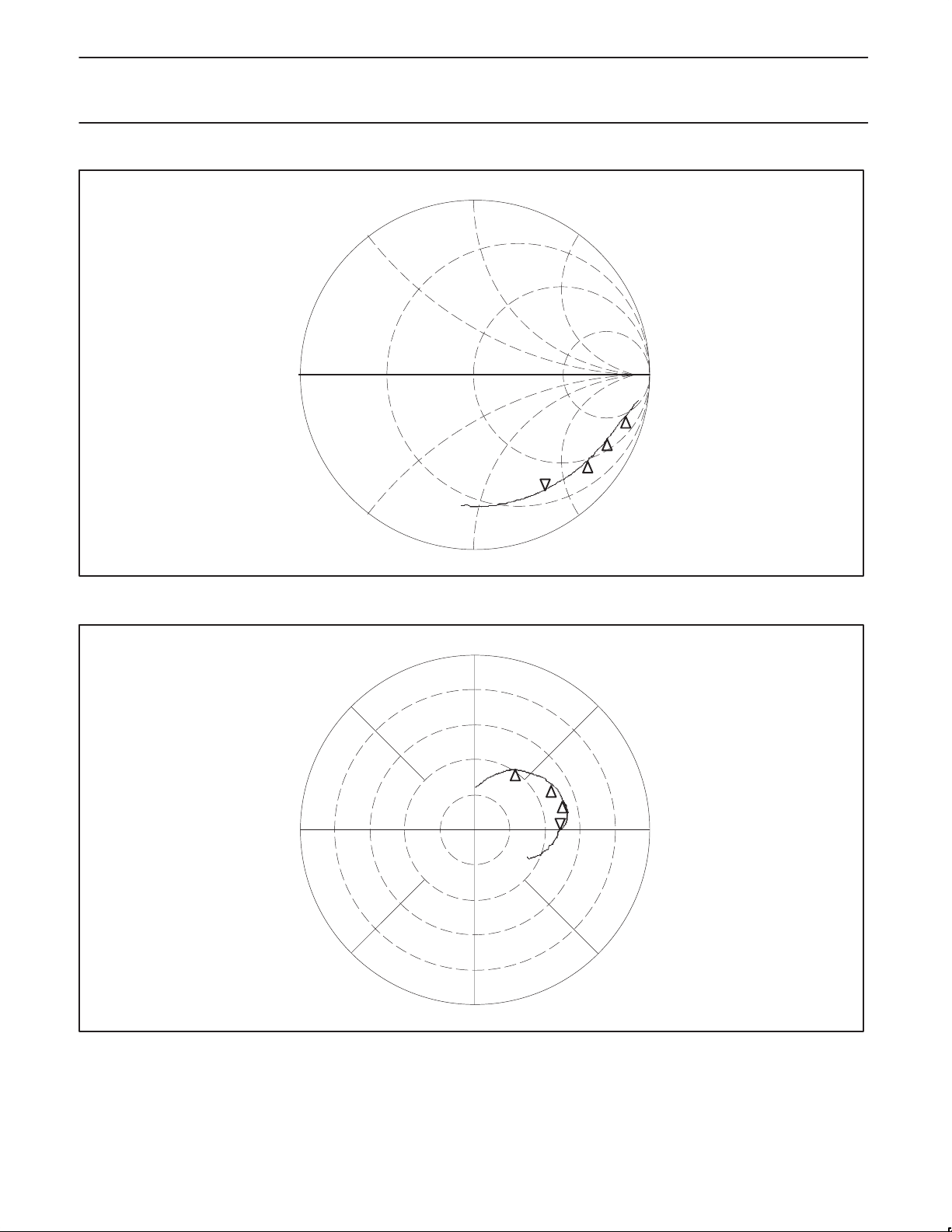
1: 133.16Ω
–326.61Ω
200MHz
2: 74.875Ω
–193.17Ω
400MHz
3: 46.625Ω
–135.03Ω
600MHz
4: 25.117Ω
–83.656Ω
2.1107pF
901.375MHz
1
2
4
3
START: 100MHz
STOP: 1.35GHz
SR01634
Figure 30. Typical S11 of Low Band LNA @ 3.75V for Receive Strong Signal Mode
1: 82.778mU
56.472°
200MHz
2: 101.74mU
30.696°
400MHz
3: 106.02mU
18.799°
600MHz
1
2
3
4
4: 97.527mU
992.89m°
901.375MHz
1999 Mar 02
START: 100MHz
STOP: 1.35GHz
SR01645
Figure 31. Typical S21 of the Low Band LNA @ 3.75V for Receive Strong Signal Mode
19
Page 20
Philips Semiconductors Product specification
SA1920Dual-band RF front-end
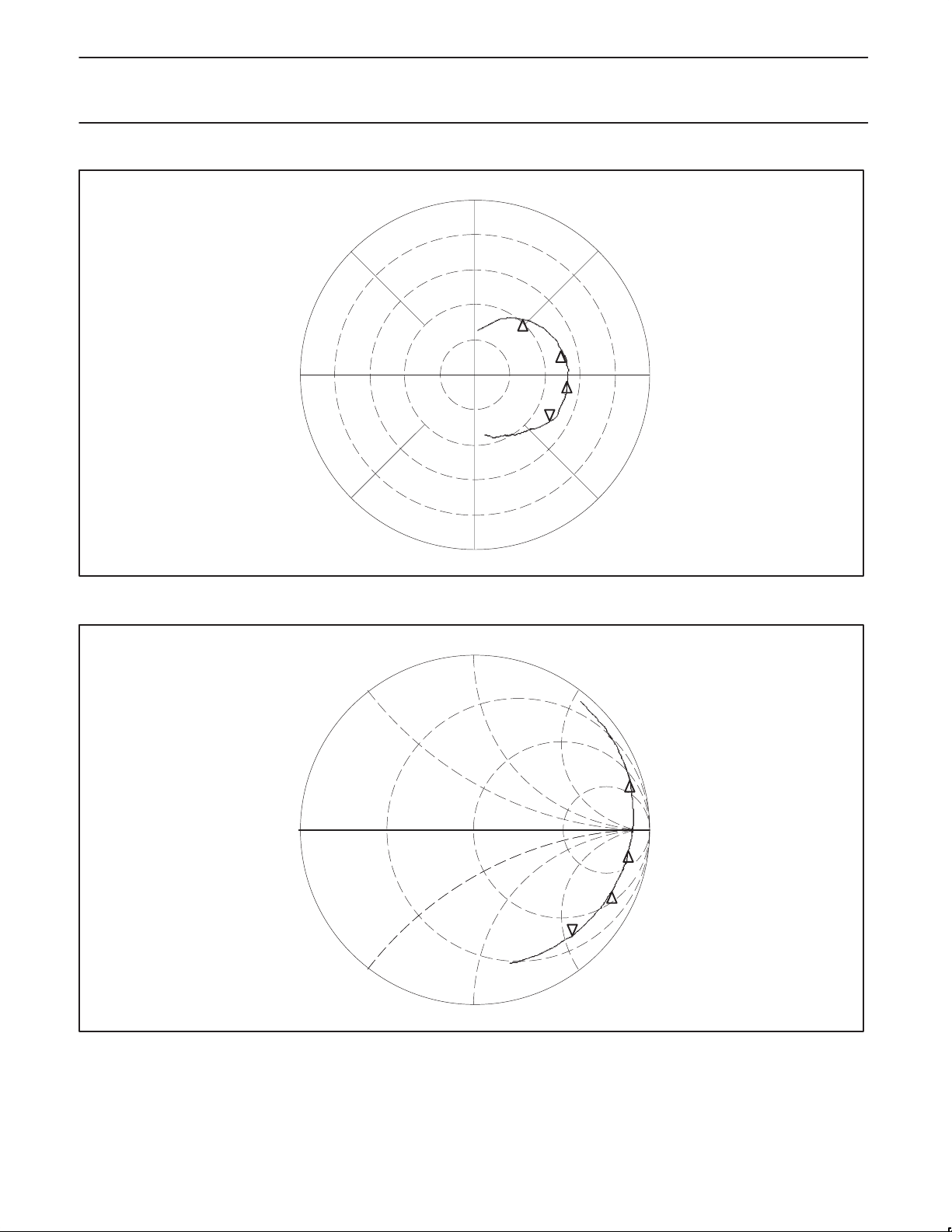
1: 82.482mU
48.834°
200MHz
2: 101.97mU
15.44°
400MHz
3: 105.45mU
–4.4673°
600MHz
4: 101.04mU
1
2
3
4
–32.816°
901.375MHz
START: 100MHz
STOP: 1.35GHz
SR01646
Figure 32. Typical S12 for the Low Band LNA @ 3.75V for the Receive Strong Signal Mode
1: 65.453Ω
303.47Ω
200MHz
2: 381.59Ω
–432.3Ω
400MHz
3: 74.375Ω
–206.25Ω
600MHz
4: 28.723Ω
1
2
3
4
–108.71Ω
1.6267pF
900MHz
1999 Mar 02
START: 100MHz
STOP: 1.35GHz
SR01635
Figure 33. Typical S22 for the Low Band LNA @ 3.75V for the Strong Receive Signal Mode
20
Page 21
Philips Semiconductors Product specification
SA1920Dual-band RF front-end
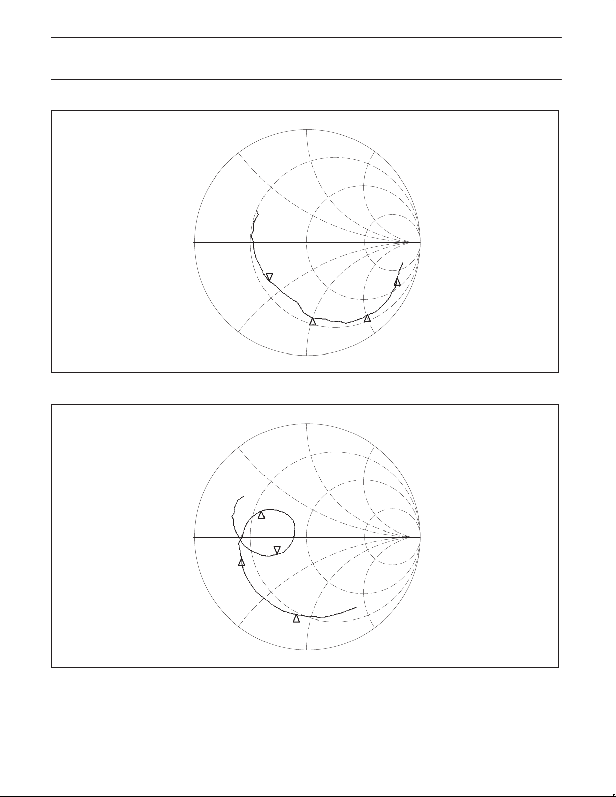
1: 102.26Ω
–217.14Ω
200MHz
2: 24.902Ω
–100.07Ω
400MHz
3: 20.596Ω
–48.596Ω
600MHz
4: 20.036Ω
–18.022Ω
9.8121pF
900MHz
4
1
2
SR01636
START: 100MHz
STOP: 1.35GHz
3
Figure 34. Typical S11 for the Low Band Mixer @ 3.75V for the Receive Normal Mode
1: 15.326Ω
–41.15Ω
200MHz
2: 12.527Ω
–7.6484Ω
400MHz
3: 19.854Ω
11.1Ω
600MHz
4: 27.865Ω
–9.7334Ω
3
4
2
18.166pF
900.125MHz
1999 Mar 02
1
START: 100MHz
STOP: 1.35GHz
SR01637
Figure 35. Typical S11 for the Low Band LO @ 3.75V for the Low Band Receive Normal Mode
21
Page 22
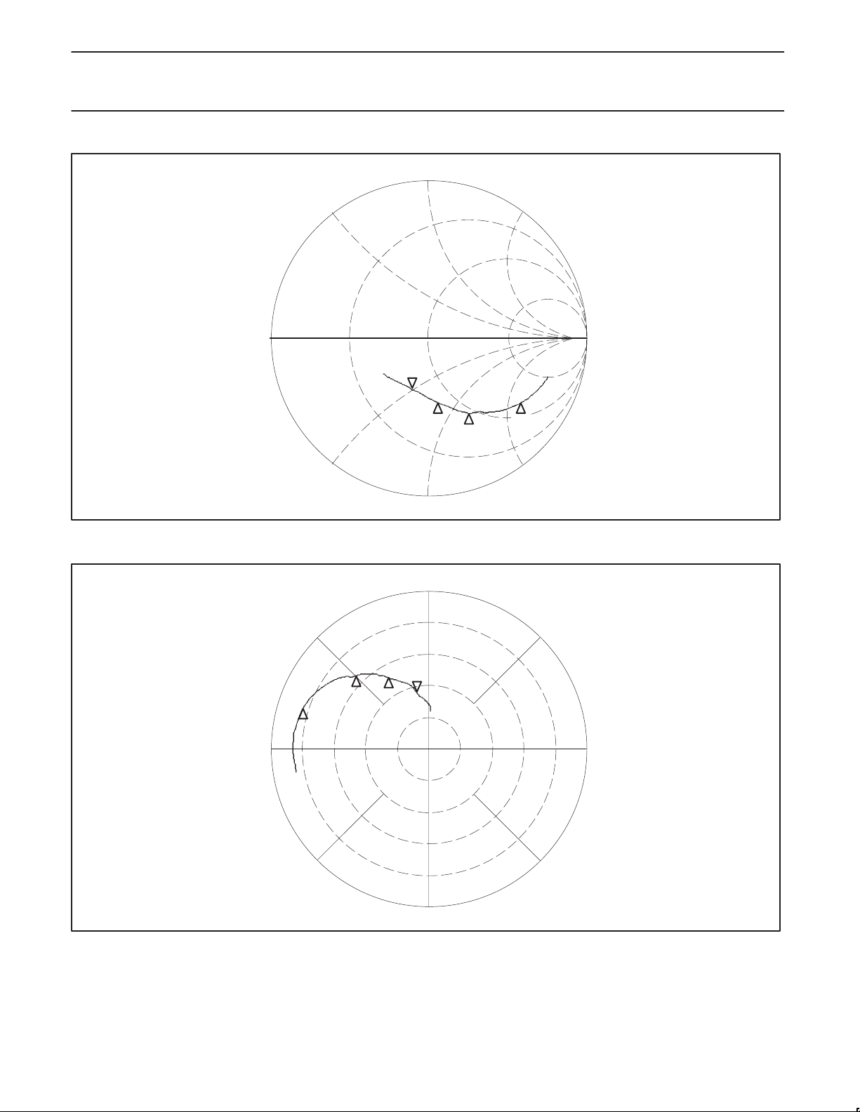
Philips Semiconductors Product specification
SA1920Dual-band RF front-end
1: 70.324Ω
–120.49Ω
200MHz
2: 45.121Ω
–61.621Ω
400MHz
3: 39.195Ω
–39.092Ω
600MHz
4: 33.025Ω
–24.061Ω
7.3497pF
900MHz
4
START: 100MHz
STOP: 1.35GHz
3
2
1
SR01638
Figure 36. Typical S11 for the Low Band LNA @ 3.75V for the Low Band Transmit (Analog) Mode
1: 16.617U
161.94°
200MHz
2: 12.974U
134.43°
400MHz
3: 10.255U
2
1
4
3
118.75°
600MHz
4: 7.3947U
101.63°
900MHz
1999 Mar 02
START: 100MHz
STOP: 1.35GHz
SR01647
Figure 37. Typical S21 of the Low Band LNA @ 3.75V for the Low Band Transmit (Analog) Mode
22
Page 23
Philips Semiconductors Product specification
SA1920Dual-band RF front-end
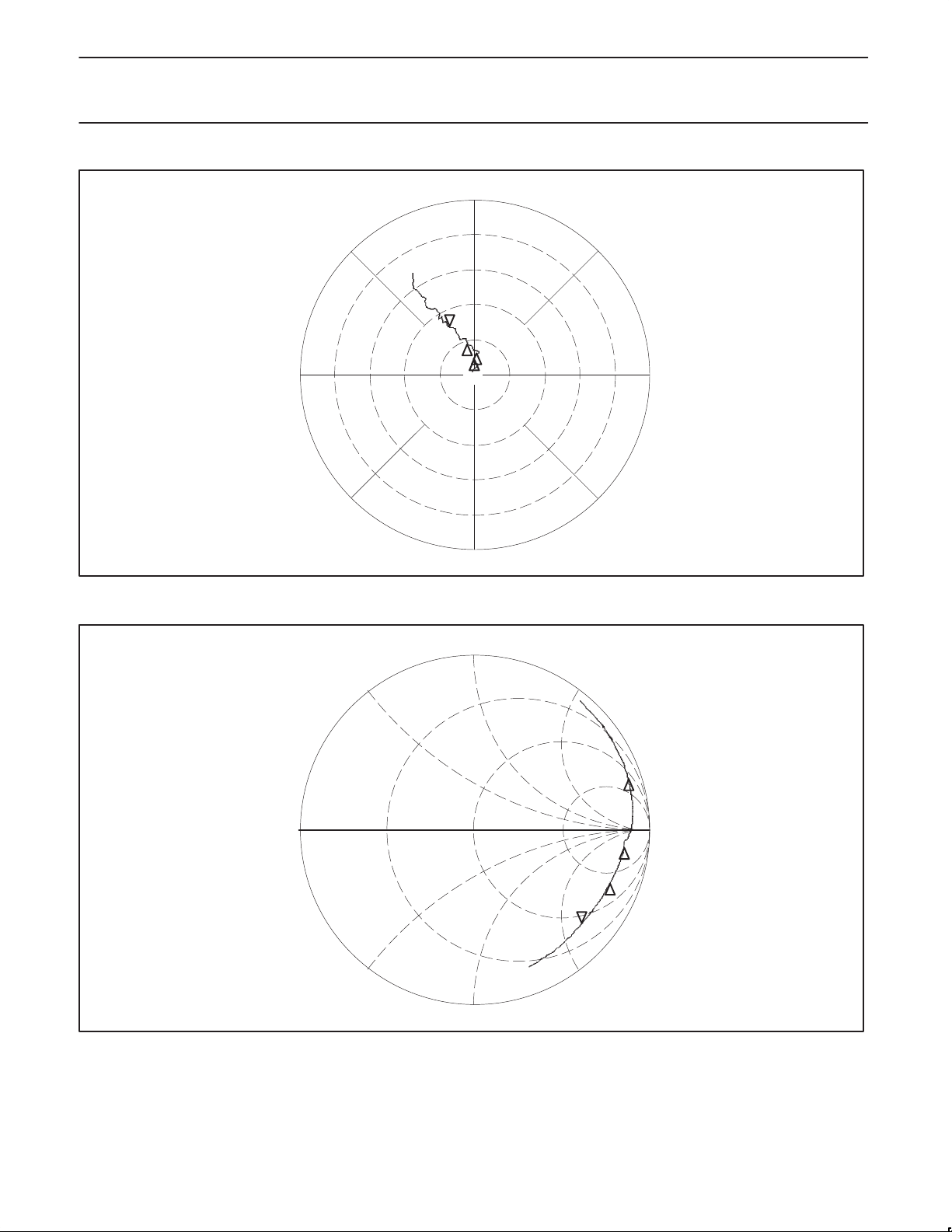
1: 4.6161mU
97.782°
200MHz
2: 6.5206mU
88.02°
400MHz
3: 9.1807mU
105.05°
4
3
2
1
600MHz
4: 15.58mU
119.06°
900MHz
START: 100MHz
STOP: 1.35GHz
SR01648
Figure 38. Typical S12 for the Low Band LNA @ 3.75V for the Low Band Transmit (Analog) Mode
1: 67.703Ω
295.39Ω
200MHz
2: 436.03Ω
–336.16Ω
400MHz
3: 105.43Ω
–216.6Ω
600MHz
4: 37.477Ω
1
2
3
4
–123.19Ω
1.4355pF
900MHz
1999 Mar 02
START: 100MHz
STOP: 1.35GHz
SR01639
Figure 39. Typical S22 for the Low Band LNA @ 3.75V for the Low Band Transmit (Analog) Mode
23
Page 24
Philips Semiconductors Product specification
SA1920Dual-band RF front-end
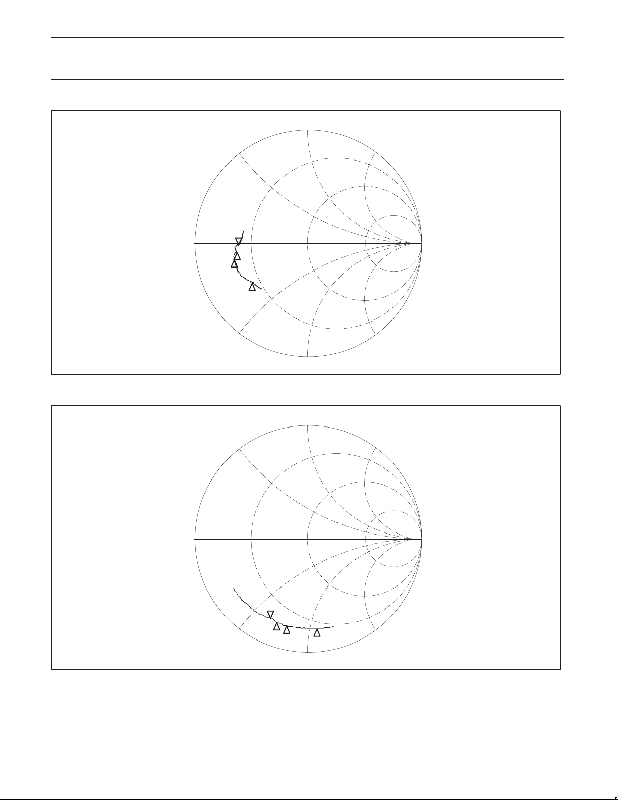
1: 13.76Ω
–15.057Ω
1.55GHz
2: 10.422Ω
–5.5498Ω
1.85GHz
3: 11.58Ω
–3.0508Ω
1.95GHz
4: 12.092Ω
–616.21mΩ
125.99pF
4
3
2
1
2.05GHz
START: 1.40GHz
STOP: 2.65GHz
SR01640
Figure 40. Typical S11 for the High Band LNA @ 3.75V for the High Band Receive Normal Mode
1: 12.135Ω
–53.891Ω
1.55GHz
2: 9.3379Ω
–38.457Ω
1.85GHz
3: 8.75Ω
–34.238Ω
1.95GHz
4: 8.7695Ω
–31.25Ω
2.4844pF
2.05GHz
4
3
START: 1.40GHz
STOP: 2.65GHz
2
1
SR01641
1999 Mar 02
Figure 41. Typical S11 for the High Band LNA @ 3.75V for the High Band Receive Strong Signal Mode
24
Page 25
Philips Semiconductors Product specification
SA1920Dual-band RF front-end
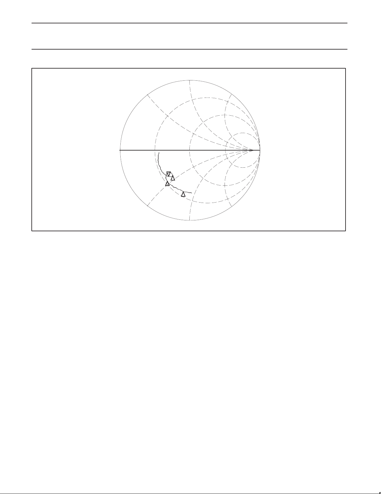
1: 20.574Ω
–38.402Ω
1.55GHz
2: 18.104Ω
–22.765Ω
1.85GHz
3: 24.446Ω
–21.71Ω
1.95GHz
4: 20.975Ω
–20.711Ω
3.7486pF
2.05GHz
4
3
2
1
START: 1.40GHz
STOP: 2.65GHz
SR01642
Figure 42. Typical S11 of the High Band LO @ 3.75V for the High Band Receive Normal Mode
1999 Mar 02
25
Page 26
Philips Semiconductors Product specification
SA1920Dual-band RF front-end
Table 2. Typical S-Parameters of Low Band LNA at VCC = +3.75V, LB Receive Normal Mode
FREQ (MHz) |S11| (U) <S11 (DEG) |S21| (U) <S21 (DEG) |S12| (U) <S12 (DEG) |S22| (U) <S22 (DEG)
100 0.89 –15.49 8.70 –165.43 0.0027 108.66 0.97 51.38
150 0.87 –22.76 8.71 –179.74 0.0038 93.41 0.96 31.54
200 0.85 –29.87 8.53 170.16 0.0049 92.10 0.96 19.54
250 0.82 –37.01 8.33 161.71 0.0065 86.08 0.95 1 1.08
300 0.79 –43.99 8.12 154.61 0.0071 82.95 0.94 4.19
350 0.75 –50.47 7.75 148.41 0.0078 69.24 0.93 –1.56
400 0.73 –56.72 7.49 144.24 0.0072 71.73 0.91 –5.69
450 0.70 –63.14 7.24 139.14 0.0078 76.99 0.91 –10.06
500 0.67 –69.13 6.97 134.34 0.0071 82.72 0.90 –13.94
550 0.63 –75.14 6.71 130.13 0.0078 84.15 0.89 –17.69
600 0.61 –81.15 6.45 126.62 0.0074 87.69 0.88 –21.14
650 0.59 –86.84 6.23 122.98 0.0079 91.07 0.88 –24.77
700 0.57 –92.30 6.03 119.16 0.0085 103.71 0.87 –28.09
750 0.55 –97.73 5.80 115.55 0.0098 103.73 0.87 –31.38
800 0.54 –102.99 5.56 11 1.56 0.0107 113.57 0.86 –34.82
850 0.53 –108.21 5.24 107.93 0.0121 1 15.45 0.86 –38.18
900 0.52 –113.27 4.97 105.40 0.0134 124.98 0.86 –41.51
950 0.51 –118.12 4.75 104.08 0.0155 127.67 0.86 –44.72
1000 0.51 –122.43 4.62 102.52 0.0175 128.87 0.86 –47.96
1050 0.51 –126.73 4.52 99.54 0.0193 128.89 0.86 –51.12
1100 0.50 –130.83 4.34 96.33 0.0217 129.85 0.86 –54.20
1150 0.51 –134.58 4.13 93.78 0.0238 128.74 0.86 –57.23
1200 0.51 –138.20 3.94 91.13 0.0269 131.20 0.86 –60.03
1250 0.51 –141.69 3.72 88.49 0.0297 130.22 0.87 –62.72
1300 0.51 –145.12 3.46 86.84 0.032 128.07 0.87 –65.57
1350 0.52 –148.25 3.25 86.69 0.033 127.73 0.87 –68.10
1999 Mar 02
26
Page 27
Philips Semiconductors Product specification
SA1920Dual-band RF front-end
Table 3. Typical S-Parameters of Low Band LNA at VCC = +3.75V, LB Strong Signal Mode
FREQ (MHz) |S11| (U) <S11 (DEG) |S21| (U) <S21 (DEG) |S12| (U) <S12 (DEG) |S22| (U) <S22 (DEG)
100 0.94 –8.77 0.05 88.15 0.049 84.08 0.96 50.15
150 0.92 –12.15 0.07 68.32 0.069 63.51 0.95 30.01
200 0.90 –15.01 0.08 55.23 0.082 47.79 0.93 17.79
250 0.88 –17.75 0.09 46.14 0.090 37.04 0.92 9.22
300 0.87 –20.37 0.09 39.25 0.094 28.09 0.91 2.68
350 0.85 –23.15 0.10 33.96 0.099 21.40 0.90 –2.68
400 0.85 –25.85 0.10 29.86 0.100 14.70 0.89 –7.56
450 0.84 –28.73 0.10 26.35 0.102 9.32 0.88 –12.06
500 0.83 –31.65 0.10 23.06 0.103 4.37 0.88 –16.23
550 0.82 –34.56 0.10 20.07 0.103 –0.41 0.87 –20.35
600 0.81 –38.02 0.10 17.87 0.103 –5.17 0.86 –24.23
650 0.80 –41.41 0.10 15.28 0.104 –9.07 0.85 –28.29
700 0.80 –44.70 0.10 12.27 0.104 –13.29 0.85 –32.11
750 0.79 –48.40 0.10 9.05 0.103 –18.00 0.84 –35.85
800 0.78 –52.30 0.10 5.24 0.103 –23.07 0.83 –39.74
850 0.78 –56.58 0.10 2.20 0.102 –28.68 0.83 –43.59
900 0.77 –60.63 0.09 –0.26 0.099 –33.94 0.82 –47.19
950 0.77 –64.88 0.09 –2.21 0.094 –39.65 0.82 –50.95
1000 0.76 –69.05 0.09 –4.19 0.090 –44.01 0.81 –54.29
1050 0.76 –73.21 0.09 –7.58 0.086 –47.95 0.81 –57.67
1100 0.76 –77.26 0.09 –11.56 0.084 –52.34 0.81 –60.86
1150 0.76 –81.34 0.08 –16.05 0.080 –58.43 0.80 –64.05
1200 0.76 –85.37 0.08 –19.50 0.076 –62.90 0.80 –66.96
1250 0.76 –89.33 0.07 –23.71 0.074 –68.35 0.80 –69.89
1300 0.76 –93.28 0.07 –27.20 0.072 –75.17 0.79 –72.64
1350 0.75 –97.37 0.06 –31.20 0.068 –82.58 0.79 –75.21
1999 Mar 02
27
Page 28
Philips Semiconductors Product specification
SA1920Dual-band RF front-end
Table 4. Typical S-Parameters of Low Band LNA at VCC = +3.75V, LB Transmit On (Analog) Mode
FREQ (MHz) |S11| (U) <S11 (DEG) |S21| (U) <S21 (DEG) |S12| (U) <S12 (DEG) |S22| (U) <S22 (DEG)
100 0.80 –18.49 16.98 –170.30 0.003 121.40 0.95 50.55
150 0.76 –27.25 17.07 173.61 0.004 100.49 0.94 30.44
200 0.72 –35.34 16.62 161.95 0.005 87.01 0.93 18.29
250 0.67 –43.14 15.82 152.47 0.005 88.74 0.92 9.80
300 0.62 –50.04 14.89 144.65 0.007 80.87 0.91 2.68
350 0.57 –55.41 13.73 138.33 0.007 64.95 0.89 –2.99
400 0.55 –61.58 12.97 134.43 0.007 90.16 0.87 –6.38
450 0.51 –67.13 12.27 129.49 0.007 90.97 0.86 –10.66
500 0.47 –72.08 11.53 125.20 0.008 89.19 0.85 –14.35
550 0.44 –76.94 10.83 121.58 0.009 96.23 0.84 –17.92
600 0.42 –81.92 10.24 118.69 0.009 98.83 0.84 –21.27
650 0.40 –86.62 9.78 115.74 0.009 102.03 0.83 –24.85
700 0.38 –91.05 9.32 112.66 0.010 107.95 0.83 –28.04
750 0.37 –95.76 8.89 109.66 0.012 108.58 0.83 –31.27
800 0.36 –100.37 8.46 106.44 0.012 114.73 0.82 –34.68
850 0.35 –105.06 7.92 103.48 0.014 115.62 0.82 –38.05
900 0.34 –109.12 7.39 101.58 0.015 116.40 0.82 –41.29
950 0.34 –113.76 7.02 100.76 0.017 116.04 0.82 –44.70
1000 0.34 –117.50 6.81 99.95 0.019 122.13 0.82 –47.58
1050 0.34 –121.31 6.64 97.57 0.021 122.61 0.83 –50.73
1100 0.34 –124.67 6.36 94.92 0.023 121.36 0.83 –53.76
1150 0.35 –127.76 6.09 92.79 0.025 123.58 0.83 –56.81
1200 0.35 –130.93 5.80 90.59 0.026 125.25 0.83 –59.62
1250 0.36 –133.78 5.48 88.25 0.030 123.53 0.84 –62.32
1300 0.36 –136.90998 5.10 87.00 0.03 122.37 0.84 –65.27
1350 0.37 –140.02216 4.82 87.05 0.03 122.64 0.85 –68.06
1999 Mar 02
28
Page 29
Philips Semiconductors Product specification
SA1920Dual-band RF front-end
Table 5. Typical S-Parameters of Low Band Mixer Input at VCC = +3.75V, LB Receive Normal Mode
FREQ (MHz) |S11| (U) <S11 (DEG)
100 0.85 –13.10
150 0.84 –17.65
200 0.85 –23.74
250 0.85 –29.63
300 0.85 –37.49
350 0.85 –45.23
400 0.85 –54.50
450 0.80 –64.14
500 0.75 –73.90
550 0.70 –82.34
600 0.67 –91.47
650 0.57 –100.54
700 0.53 –106.44
750 0.51 –114.37
800 0.49 –123.87
850 0.48 –132.17
900 0.49 –141.42
950 0.47 –150.07
1000 0.47 –160.64
1050 0.47 –169.49
1100 0.47 –179.79
1150 0.48 171.14
1200 0.48 162.01
1250 0.49 154.08
1300 0.50 144.55
1350 0.51 136.1 1
1999 Mar 02
29
Page 30
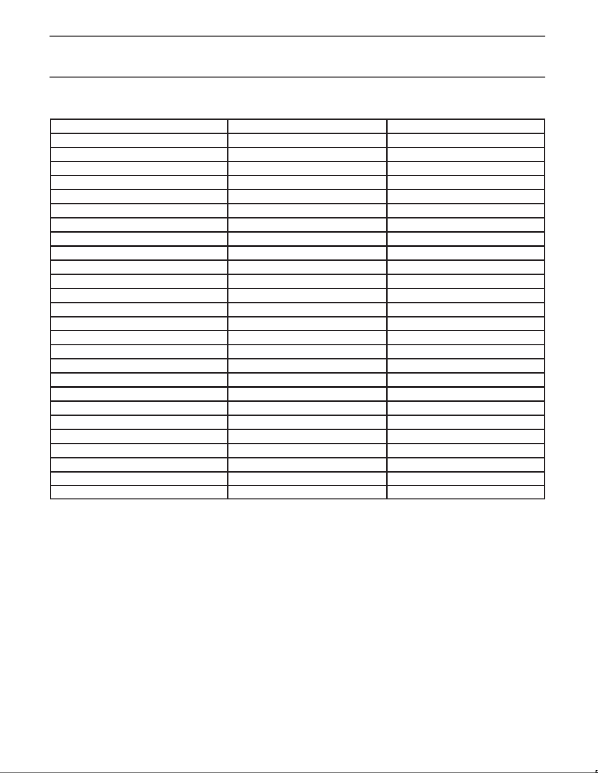
Philips Semiconductors Product specification
SA1920Dual-band RF front-end
Table 6. Typical S-Parameters of Low Band LO Input at VCC = +3.75V, LB Receive Normal Mode
FREQ (MHz) |S11| (U) <S11 (DEG)
100 0.76 –55.83
150 0.73 –78.35
200 0.70 –98.64
250 0.68 –116.73
300 0.66 –133.17
350 0.64 –147.82
400 0.61 –161.51
450 0.59 –173.68
500 0.55 173.99
550 0.51 162.15
600 0.46 150.30
650 0.38 140.69
700 0.29 132.76
750 0.18 131.71
800 0.10 171.44
850 0.18 –150.19
900 0.31 –149.41
950 0.42 –157.78
1000 0.50 –166.73
1050 0.57 –175.14
1100 0.61 177.49
1150 0.64 170.74
1200 0.66 164.22
1250 0.68 157.61
1300 0.68 150.89
1350 0.65 144.80
1999 Mar 02
30
Page 31
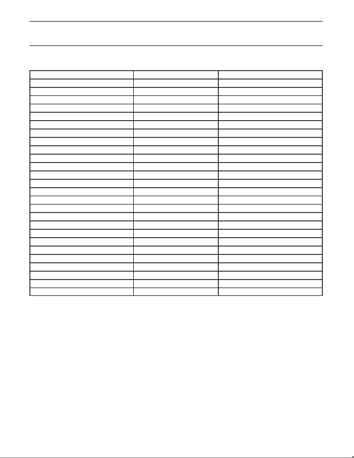
Philips Semiconductors Product specification
SA1920Dual-band RF front-end
Table 7. Typical S-Parameters of HB LNA Input at VCC = +3.75V, HB Receive Normal Mode
FREQ (MHz) |S11| (U) <S11 (DEG)
1400 0.58 –135.43
1450 0.59 –138.48
1500 0.59 –141.42
1550 0.60 –144.44
1600 0.62 –146.93
1650 0.63 –149.85
1700 0.65 –154.08
1750 0.66 –158.38
1800 0.66 –162.67
1850 0.66 –167.09
1900 0.65 –170.72
1950 0.63 –172.76
2000 0.64 –175.38
2050 0.61 –178.44
2100 0.60 –179.38
2150 0.59 179.32
2200 0.58 178.44
2250 0.58 177.61
2300 0.57 176.29
2350 0.57 175.39
2400 0.57 174.35
2450 0.56 173.01
2500 0.57 172.12
2550 0.57 170.91
2600 0.56 169.89
2650 0.56 168.41
1999 Mar 02
31
Page 32
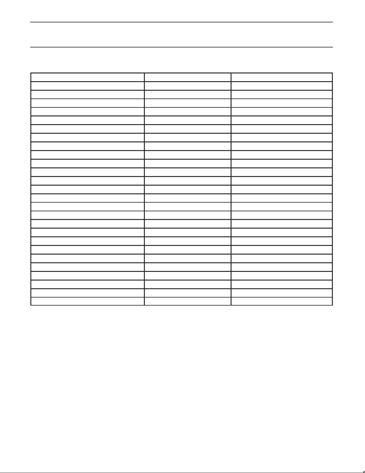
Philips Semiconductors Product specification
SA1920Dual-band RF front-end
Table 8. Typical S-Parameters of HB LNA Input at VCC = +3.75V, HB Strong Signal Mode
FREQ (MHz) |S11| (U) <S11 (DEG)
1400 0.81 –73.99
1450 0.81 –77.23
1500 0.81 –80.62
1550 0.80 –84.00
1600 0.80 –87.02
1650 0.80 –90.35
1700 0.79 –93.54
1750 0.79 –96.48
1800 0.79 –100.32
1850 0.79 –103.54
1900 0.79 –107.23
1950 0.79 –110.05
2000 0.77 –113.75
2050 0.78 –114.79
2100 0.79 –117.61
2150 0.79 –120.50
2200 0.80 –122.65
2250 0.79 –125.91
2300 0.80 –128.17
2350 0.79 –130.64
2400 0.79 –133.19
2450 0.79 –135.66
2500 0.79 –138.22
2550 0.79 –140.56
2600 0.79 –143.22
2650 0.79 –145.47
1999 Mar 02
32
Page 33
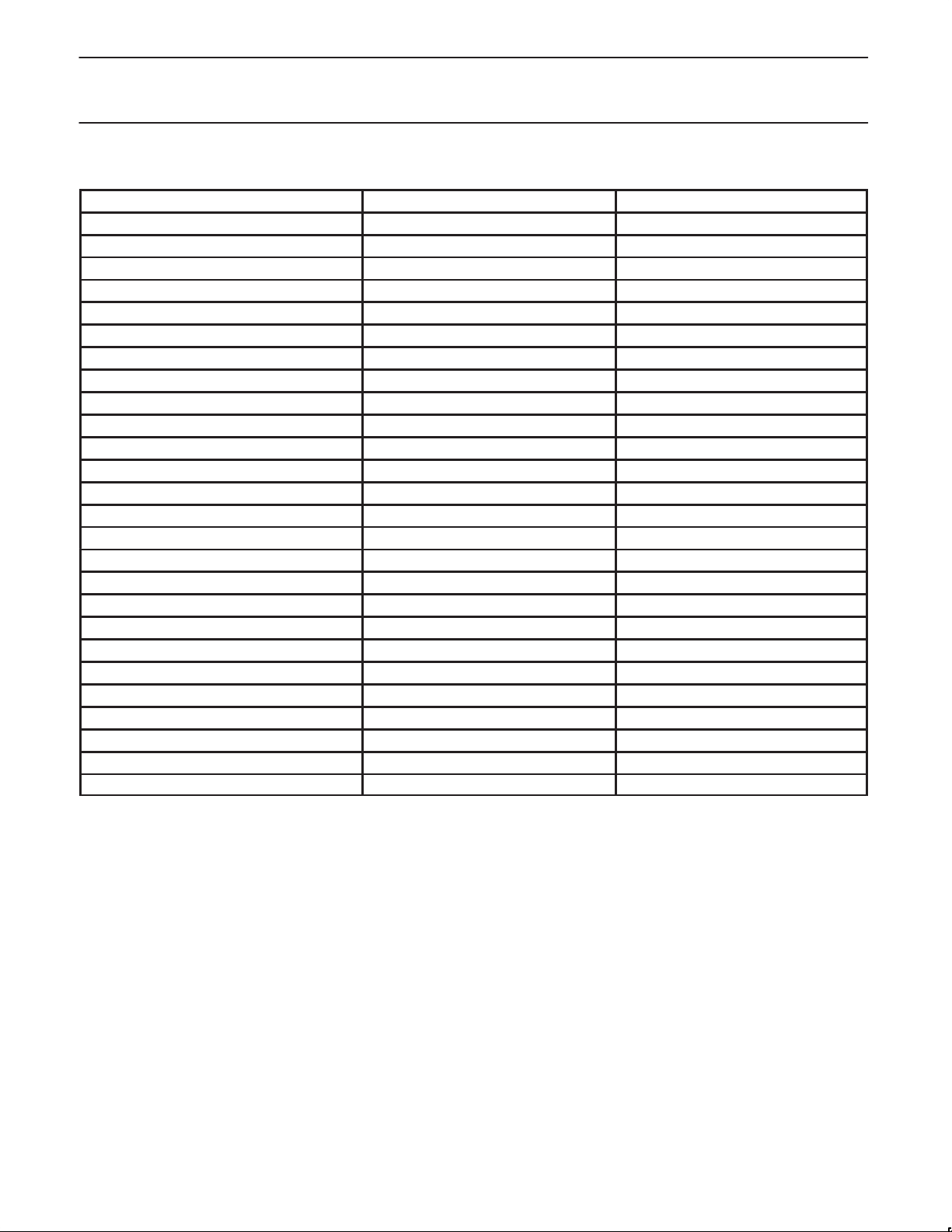
Philips Semiconductors Product specification
SA1920Dual-band RF front-end
Table 9. Typical S-Parameters of HB LO Input at VCC = +3.75V, HB Receive Normal Mode
FREQ (MHz) |S11| (U) <S11 (DEG)
1400 0.62 –87.50
1450 0.61 –90.87
1500 0.60 –94.44
1550 0.60 –98.86
1600 0.59 –102.10
1650 0.59 –106.34
1700 0.58 –110.67
1750 0.57 –114.48
1800 0.57 –119.86
1850 0.55 –126.14
1900 0.48 –134.66
1950 0.43 –123.95
2000 0.47 –126.26
2050 0.48 –128.33
2100 0.50 –131.34
2150 0.50 –135.52
2200 0.50 –138.76
2250 0.50 –142.68
2300 0.50 –146.60
2350 0.49 –150.21
2400 0.49 –154.30
2450 0.48 –157.62
2500 0.47 –161.79
2550 0.46 –166.32
2600 0.45 –170.41
2650 0.43 –174.86
1999 Mar 02
33
Page 34
Philips Semiconductors Product specification
SA1920Dual-band RF front-end
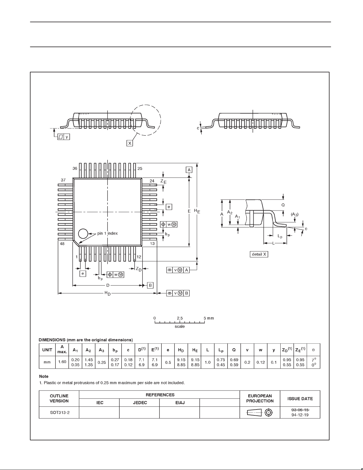
LQFP48: plastic low profile quad flat package; 48 leads; body 7 x 7 x 1.4 mm SOT313-2
1999 Mar 02
34
Page 35

Philips Semiconductors Product specification
SA1920Dual-band RF front-end
NOTES
1999 Mar 02
35
Page 36

Philips Semiconductors Product specification
SA1920Dual-band RF front-end
Data sheet status
Data sheet
status
Objective
specification
Preliminary
specification
Product
specification
Product
status
Development
Qualification
Production
Definition
This data sheet contains the design target or goal specifications for product development.
Specification may change in any manner without notice.
This data sheet contains preliminary data, and supplementary data will be published at a later date.
Philips Semiconductors reserves the right to make chages at any time without notice in order to
improve design and supply the best possible product.
This data sheet contains final specifications. Philips Semiconductors reserves the right to make
changes at any time without notice in order to improve design and supply the best possible product.
[1]
[1] Please consult the most recently issued datasheet before initiating or completing a design.
Definitions
Short-form specification — The data in a short-form specification is extracted from a full data sheet with the same type number and title. For
detailed information see the relevant data sheet or data handbook.
Limiting values definition — Limiting values given are in accordance with the Absolute Maximum Rating System (IEC 134). Stress above one
or more of the limiting values may cause permanent damage to the device. These are stress ratings only and operation of the device at these or
at any other conditions above those given in the Characteristics sections of the specification is not implied. Exposure to limiting values for extended
periods may affect device reliability.
Application information — Applications that are described herein for any of these products are for illustrative purposes only. Philips
Semiconductors make no representation or warranty that such applications will be suitable for the specified use without further testing or
modification.
Disclaimers
Life support — These products are not designed for use in life support appliances, devices or systems where malfunction of these products can
reasonably be expected to result in personal injury . Philips Semiconductors customers using or selling these products for use in such applications
do so at their own risk and agree to fully indemnify Philips Semiconductors for any damages resulting from such application.
Right to make changes — Philips Semiconductors reserves the right to make changes, without notice, in the products, including circuits, standard
cells, and/or software, described or contained herein in order to improve design and/or performance. Philips Semiconductors assumes no
responsibility or liability for the use of any of these products, conveys no license or title under any patent, copyright, or mask work right to these
products, and makes no representations or warranties that these products are free from patent, copyright, or mask work right infringement, unless
otherwise specified.
Philips Semiconductors
811 East Arques Avenue
P.O. Box 3409
Sunnyvale, California 94088–3409
Telephone 800-234-7381
Copyright Philips Electronics North America Corporation 1999
All rights reserved. Printed in U.S.A.
Date of release: 03–99
Document order number: 9397 750 05354
1999 Mar 02
36
 Loading...