

Page 1

INTEGRATED CIRCUITS
SA1638
Low voltage IF I/Q transceiver
Product specification 1997 Sept 03
IC17 Data Handbook
Page 2
Philips Semiconductors Product specification
SA1638Low voltage IF I/Q transceiver
DESCRIPTION
The SA1638 is a combined Rx and Tx IF I/Q circuit. The receive
path contains an IF amplifier, a pair of quadrature down-mixers, and
a pair of baseband filters and amplifiers. A second pair of mixers in
the transmit path transposes a quadrature baseband input up to the
IF frequency. An external VCO signal is divided down internally and
buffered to provide quadrature local oscillator signals for the mixers.
A further divider chain, reference divider and phase detector are
provided to avoid the need for an external IF synthesizer. Rx or Tx
path or the entire circuit may be powered down by logic inputs.
On-board voltage regulators are provided to allow direct connection
to a battery supply.
FEATURES
•Direct supply: 3.3V to 7.5V
•Two DC regulators giving 3.0V output
•Low current consumption: 18mA for Rx or 22mA for Tx
•Input/output IF frequency from 70-400 MHz
•Internal IF PLL for synthesizing the local oscillator signal
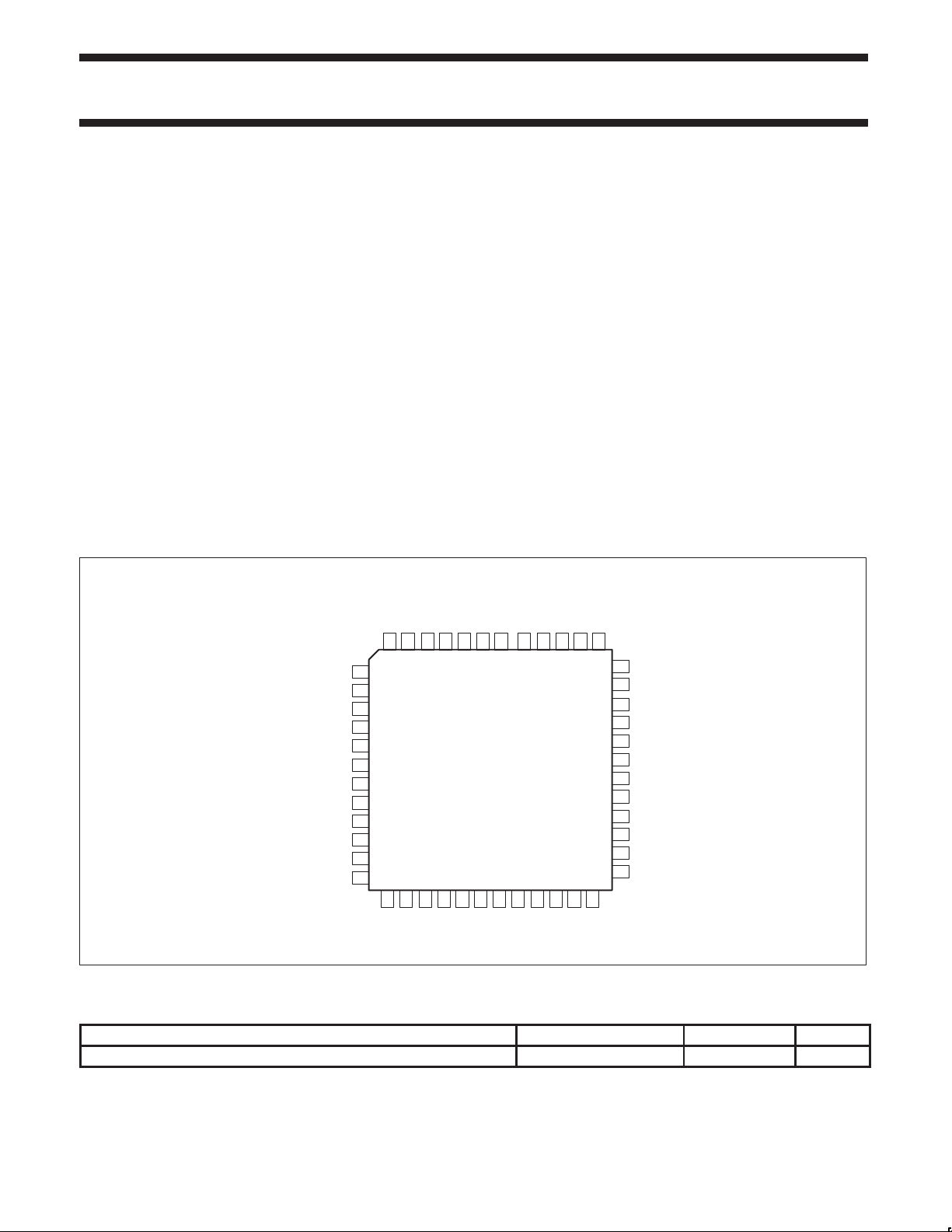
PIN CONFIGURATION
GNDREG1
VccTxRx
GND1
VREG1
1
VREG2
PON
V
BATT
AOUT
BOUT
DCRES
RESD
RESA
RESB
2
3
4
5
6
7
8
9
10
11
12
13 14 15 16 17 18 19
VREGF2
GNDREG2
•High performance on-board integrated receive filters with
•Switchable alternative bandwidth setting available to allow
•Designed for a widely used I and Q baseband GSM interface
•Control registers power up in a default state
•Optional DC offset trim capability to <200mV
•Only a standard reference input frequency required, choice of 13,
•Fully compatible with SA1620 GSM RF front-end (see Figure 9)
APPLICATIONS
•IF circuitry for GSM 900MHz hand-held units
•IF circuitry for PCN (DCS1800) hand-held units
•Quadrature up and down mixer stage
LQFP Package
RxIF IN
RxIF INX
45464748
GND2
424344
48–pin LQFP
bandwidth tunable between 50-850 kHz
channel bandwidth flexibility in operation
26, 39 or 52MHz
TxIFOUT
TxIFOUTX
GND3
PONPLL
VccCP
394041 3738
20 21 22 23 24
CP
36
35
34
33
32
31
30
29
28
27
26
25
VEECP
I
REF
LO INX
LO IN
ADJ IN
CLK IN
CLK INX
LOCK
STROBE
CLOCK
DATA
V
DIG
EE
V
PONRx
REF
QRxOUT
QRxOUTX
IRxOUT
IRxOUTX
QTx IN
QTx INX
ITx IN
PDTx
ITx INX
VccDIG
SR00524
Figure 1. SA1638 Pin Configuration
ORDERING INFORMATION
DESCRIPTION TEMPERATURE RANGE ORDER CODE DWG #
48-Pin Thin Quad Flat Pack (LQFP)
1997 Sept 03 853-1818 18351
2
-40 to +85°C
SA1638BE SOT313-2
Page 3
Philips Semiconductors Product specification
SA1638Low voltage IF I/Q transceiver
BLOCK DIAGRAM
PONRx
V
REF
PDTx
TxIFOUT
TxIFOUTX
VCCTxRx
GND3
GND1
RxIF IN
RxIF INX
GND2
LO IN
LO INX
ADJ IN
LOCK
I
REF
PONPLL
V
CC
V
EE
CP
CP
CP
RESA
IF
AMP
RESB
BIAS RX
BIAS TX
CHARGE
PUMP
VREG1
RESD
2
÷
BUFFERS
DETECTOR
÷
GNDREG1
V.REG.1 V.REG.2
N
÷
PHASE
13, 26
39, 52
BATT
V
DC
ADJUST
DC
REGISTER
TEST
REGISTER
SYNTH
REGISTER
PON
VREGF2
GNDREG2
STATUS
REGISTER
SERIAL
INPUT
VREG2
ITx IN
ITx INX
QTx IN
QTx INX
IRxOUT
IRxOUTX
QRxOUT
QRxOUTX
DCRES
AOUT
BOUT
1997 Sept 03
V
DIG
CC
V
DIG
EE
CLK IN
CLK INX
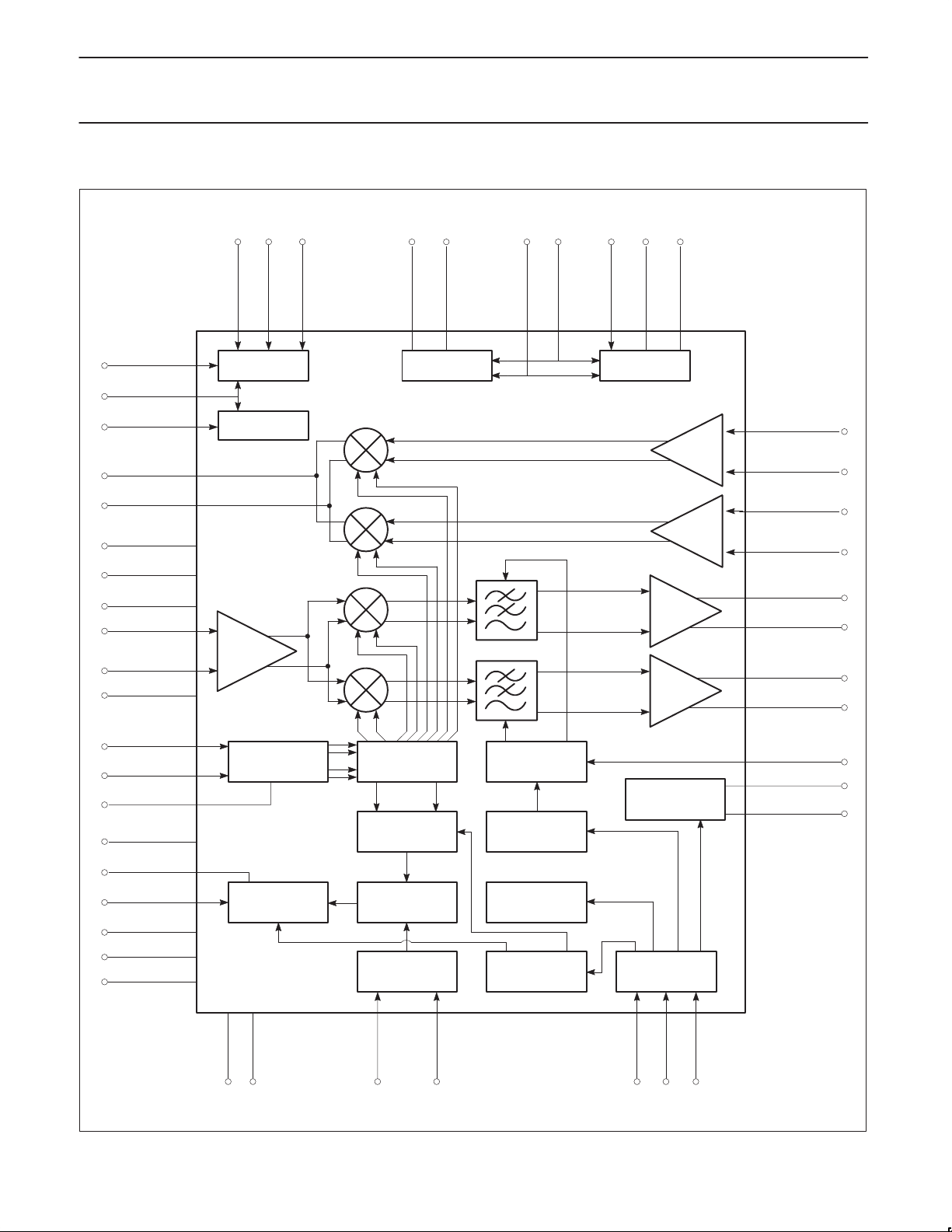
Figure 2. SA1638 Block Diagram
3
DATA
CLOCK
STROBE
SR00525
Page 4
Philips Semiconductors Product specification
SA1638Low voltage IF I/Q transceiver
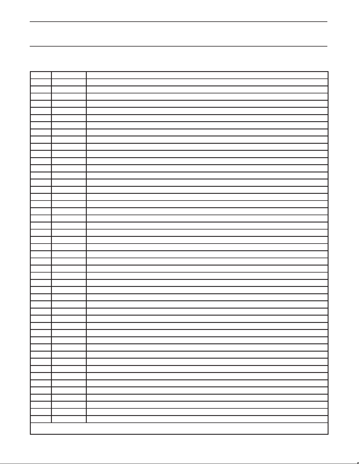
PIN DESCRIPTIONS
Pin No. Pin Name Description
1 VREG1 Output voltage of regulator 1
2 VREGF2 Feedback of regulator 2
3 VREG2 Output voltage of regulator 2
4 GNDREG2 Ground of regulator 2
5 PON Power-on input for voltage regulators 1 and 2 (active high)
6 V
BATT
7 AOUT Programmable logic output (see Figure 9)
8 BOUT Programmable logic output (see Figure 9)
9 DCRES Reference current setting resistor for DC offset circuit
10 RESD Additional external current defining resistor for filters
11 RESA Principal external current defining resistor for filters
12 RESB Principal external current defining resistor for filters
13 PONRx Power-on input for Rx (active high)
14 V
15 QRxOUT Differential receive baseband output
16 QRxOUTX Differential receive baseband output
17 IRxOUT Differential receive baseband output
18 IRxOUTX Differential receive baseband output
19 QTx IN Differential transmit baseband input
20 QTx INX Differential transmit baseband input
21 ITx IN Differential transmit baseband input
22 ITx INX Differential transmit baseband input
23 PDTx Power-on for transmitter (active low)
24 VCCDIG Digital circuit supply
25 VEEDIG Digital ground
26 DATA Serial bus data input
27 CLOCK Serial bus clock input
28 STROBE Serial bus strobe input
29 LOCK Test control/synthesizer lock indicator
30 CLK INX Differential reference divider input
31 CLK IN Differential reference divider input
32 ADJ IN Used for test only. Do not connect
33 LO IN Differential LO input
34 LO INX Differential LO input
35 I
36 VEECP Charge pump ground
37 CP Charge pump output
38 VCCCP Charge pump circuit supply
39 POnPLL Power-on input for synthesizer circuits (active high)
40 GND3 Ground (internal connection to GND1 and GND2)
41 TxIFOUTX Differential transmit IFoutput (open collector)
42 TxIFOUT Differential transmit IFoutput (open collector)
43 GND2 Ground (internal connection to GND1 and GND3)
44 RxIF INX Differential receive IF input
45 RxIF IN Differential receive IF input
46 GND1 Ground (internal connection to GND2 and GND3)
47 VCCTxRx Transmit and receive circuits supply voltage (also feedback of Regulator 1)
48 GNDREG1 Ground of regulator 1
NOTE: There are no ESD protection diodes at Pins 41 and 42. Thus, open collector outputs may have increased DC voltage or higher AC
peak voltage.
REF
REF
Input voltage for regulators 1 and 2
Reference voltage
Reference current setting for charge pump
1997 Sept 03
4
Page 5
Philips Semiconductors Product specification
SYMBOL
PARAMETER
TEST CONDITIONS
UNITS
SA1638Low voltage IF I/Q transceiver
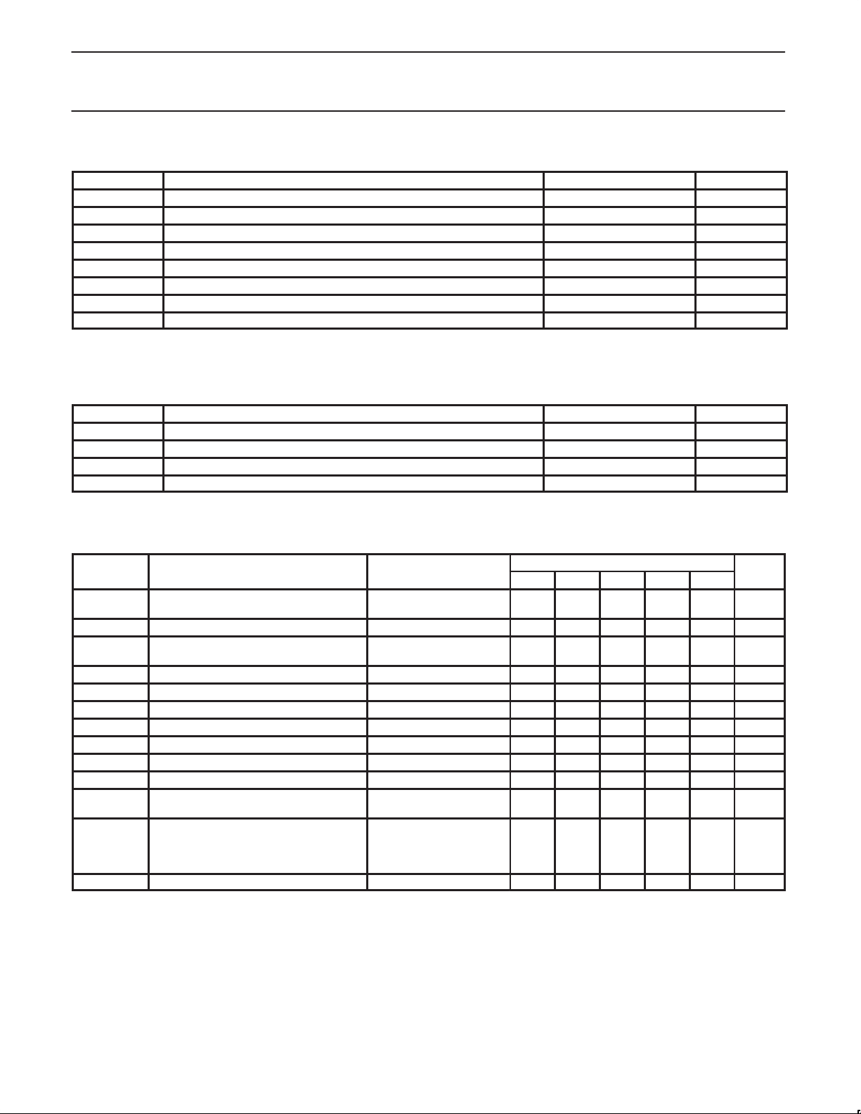
ABSOLUTE MAXIMUM RATINGS
SYMBOL PARAMETER RATING UNITS
VCCXXX Supply voltages: VCCTxRx, VCCDIG, VCCCP -0.3 to +6.0 V
V
BATT
V
IN
∆VG Any GND pin to any other GND pin 0 V
P
D
T
JMAX
P
MAX
T
STG
NOTE:
1. Maximum dissipation is determined by the operating ambient temperature and the thermal resistance, θ
RECOMMENDED OPERATING CONDITIONS
SYMBOL PARAMETER RATING UNITS
VCCXXX Supply voltages: VCCTxRx, VCCDIG 2.7 to 5.5 V
VCCCP Charge pump supply voltage 2.9 to 5.5 V
V
BATT
T
A
Battery voltage -0.3 to +8.0 V
Voltage applied to any other pin -0.3 to (V
+0.3) V
CCXXX
Power dissipation, TA = 25°C (still air) 300 mW
Maximum operating junction temperature 150 °C
Maximum power input/output +20 dBm
Storage temperature range –65 to +150 °C
. 48-pin LQFP: θJA = 67°C/W.
JA
Battery voltage 3.3 to 7.5 V
Operating ambient temperature range -40 to +85 °C
Voltage Regulators
TA = 25°C, PON = 3V, PONRX = 0V, PDTX = 3V, PONPLL = 0V, V
connected to V
V
1,
REG
V
2
REG
V
BATT
I
1, I
OUT
OUT
I
BATT
I
BATT PD
2
C
1
REG
2
C
2
REG
F2; VCCDIG = VCCCP = 3V; unless otherwise stated.
REG
Nominal V
Maximum output current for each
2
regulator
OUT
1
Supply current for both regulators I
Power-down supply current PON = 0V, I
V
1 cap load 0.1 1000 µF
REG
V
2 cap load 0.1 500 µF
REG
LINEREG Line regulation DC, V
LOADREG Load regulation I
BW Bandwidth 100 kHz
F
F
PON
REG
t
ON
Feedthrough attenuation from PON to
each regulator
Feedthrough attenuation from V
each regulator
BATT
to
Turn ON time 10 µs
NOTES:
1. At T
≥ 150°C a thermal switch reduces the output current to avoid damage.
j
2. Recommended load capacitors: In every case C
optional ≤1000µF with series resistance ≤5Ω. The low series resistance is very important to ensure regulator stability.
REG
1 = C
3. Standard deviations are based on the characterization results of 90 ICs.
BATT
= 3.3V, I
OUT
1 = I
2 = 15mA, V
OUT
1 connected to VCCTxRx, V
REG
LIMITS
Min –3σ Typ +3σ Max
2.85 2.93 3.00 3.07 3.15 V
3.3 7.5 V
= 0mA 4.3 5 5.7 7 mA
LOAD
= 0mA 7.7 9 10.3 15 µA
LOAD
= 3.3V to 7.5V –0.4 –0.2 0.001 0.2 0.4 %
BATT
= 15mA to 30mA –5 –0.37 -0.17 0.03 5 %
LOAD
≤ -40 dB
f ≤ 100kHz
f = 10MHz
f = 100MHz
f = 400MHz
2 = 100nF to ground with series resistance ≤0.1Ω. Additional capacitor
REG
≤ -61
≤ -32
≤ -37
≤ -48
REG
30 mA
dB
2
1997 Sept 03
5
Page 6
Philips Semiconductors Product specification
SYMBOL
PARAMETER
TEST CONDITIONS
UNITS
SYMBOL
PARAMETER
TEST CONDITIONS
UNITS
SA1638Low voltage IF I/Q transceiver
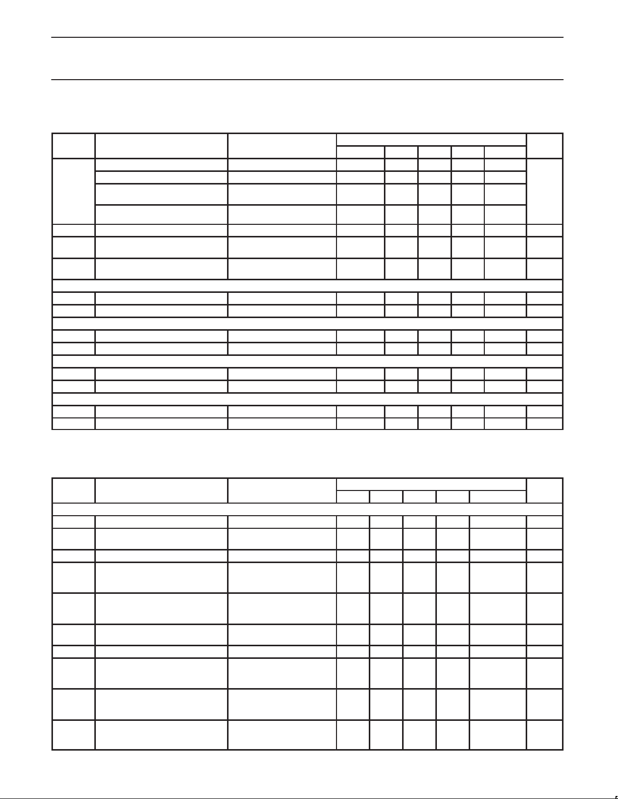
DC ELECTRICAL CHARACTERISTICS
VCCTxRx=VCCDIG=VCCCP=PONRx=PONPLL= +3V; VEEDIG = VEECP=GND1=GND2=GND3=PDTx = 0V; TA = 25°C, unless otherwise stated.
LIMITS
MIN –3σ TYP +3σ MAX
Supply current
Rx and IF synthesizer active
I
CC
Tx and IF synthesizer active
Power-down mode
IV
V
I
OUT
Reference voltage Generated internally 1.39 1.57 1.75 V
REF
V
REF
REFISINK
I
SOURCE
DC output current
Digital inputs (PON)
V
V
High level input voltage range 2.0 V
IH
Low level input voltage range 0 0.8 V
IL
Digital inputs (PDTx, PONRx, PONPLL, PON)
V
V
High level input voltage range 2.0 VCCTxRx V
IH
Low level input voltage range 0 0.8 V
IL
Digital inputs (Clock, Data, Strobe)
V
V
High level input voltage range 2.0 VCCDig V
IH
Low level input voltage range 0 0.8 V
IL
Digital outputs (LOCK, AOUT, BOUT)
V
V
Output voltage HIGH IO = -2mA
OH
Output voltage LOW IO = 2mA 0.4 V
OL
PONRx = PONPLL = PDTx = Hi
PONRx = PDTx = Low;
PONPLL = Hi
PONRx = PONPLL = Low;
PDTx = Hi
At pins TxIFOUT and
TxIFOUTX
14.4 16 17.6 20
17.4 19.5 21.6 24
0.068
5
5
1.5 1.86 2.0 2.14 2.7 mA
BATT
VCCDIG–0.4
mA
µA
V
V
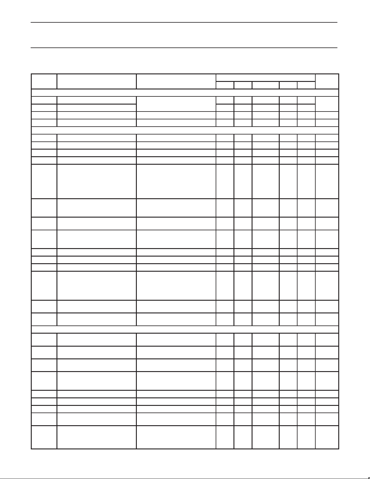
AC ELECTRICAL CHARACTERISTICS
VCCTxRx=VCCDIG=VCCCP=PONRx=PONPLL= +3V; VEEDIG = VEECP=GND1=GND2=GND3=PDTx = 0V; LOIN = 100mV
CLK
= 100mV
IN
, 52MHz; serial registers programmed with default values; TA = 25°C unless otherwise stated. Test Circuit Figure 8.
PEAK
LIMITS
MIN –3σ TYP +3σ MAX
IF Transmit Modulator
BW Input modulation bandwidth 200Ω source impedance 0.82 0.94 1.06 MHz
V
COM
V
IN
Common mode range for
baseband inputs
Peak input signal amplitude Centered on V
Third harmonic distortion
1
DC at pins ITxIN, ITxINx,
QTxIN, QTxINx
COM
| ITxIn | = | ITxInX | =
| QTxIn | = | QTxInX |
= 0.75V
PEAK;
fin = 20kHz
1 1.5 2 V
0.75 V
-61 -57 -53 -40 dB
Between pins: ITxIn and
R
C
INTx
INTx
Input resistance
Input capacitance
ITxInX or QTxIn and
QTxInX
At ITxIn, ITxInX,
QTxIn, QTxInX
112 kΩ
Output saturation limit VCCTxRx-0.3 V
| ITxIn | = | ITxInX | =
I
OUT
S
RMS output current
LO suppression
LO
1
SSB Sideband suppression
1
| QTxIn | = | QTxInX |
= 0.75V
PEAK
| ITxIn | = | ITxInX | =
| QTxIn | = | QTxInX |
= 0.75V
PEAK
; fin = 20k
| ITxIn | = | ITxInX | =
| QTxIn | = | QTxInX |
= 0.75V
PEAK
; fin = 20k
0.6 0.73 0.82 0.91 1.08 mA
+30 +43 dB
+35 +50 dB
, 800MHz;
PEAK
10 pF
1997 Sept 03
6
Page 7
Philips Semiconductors Product specification
SYMBOL
PARAMETER
TEST CONDITIONS
UNITS
dBc/H
SA1638Low voltage IF I/Q transceiver
AC ELECTRICAL CHARACTERISTICS (Continued)
LIMITS
MIN –3σ TYP +3σ MAX
IF Transmit Modulator (continued)
t
t
OFF
Noise density at 600kHz
Noise density at 10MHz
Turn ON time PdTx = LO, transmit signal to 90% 5 µs
ON
Turn OFF time PdTx = HI, transmit signal to 10% 5 µs
|ITxIn| = |ITxInX| = |QTxIn| =
|QTxInX| = 0.75V
PEAK -133 -131 -129
IF Receiver (R = 36kΩ between pins RESA and RESB)
RInRx Differential input impedance fIN = 400MHz 5 || 0.6 kΩ || pF
ROutRx Output impedance 1 kΩ
Output common mode voltage V
f3dB Low pass filter -3dB bandwidth 70 83 90 kHz
Low pass filter attenuation:
200kHz
400kHz
600kHz
6.5MHz
13.0MHz
Differential output PD into GSM
VG Voltage gain
baseband relative to 1200Ω
source EMF
NF Noise figure
8
1200Ω source and external
matching resistor and inductor
Channel matching:
Gain
fIN = 400.005MHz
Phase
2
Differential, DCRES=562kΩ -60 -25 60 mV
I
V
OUT
OUT
Output DC offset
Output drive current at each pin Source (Sink) 10 (700) µA
Minimum differential output swing 2.0 V
Input 1dB compression point:
In band
P
-1dB
200kHz
400kHz
1200Ω source EMF
600kHz
t
t
OFF
ON
Turn ON time
Turn OFF time
3
POnRx = HI, to baseband signal
out
POnRx = LO, to no baseband
signal out
IF Synthesizer
Local oscillator input frequency
LO
range
9
Differential input impedance
LO peak input voltage range
Between pins LOIN and LOINX, f
= 800MHz
Single-ended
Referred to 50Ω
IN
Z
V
f
LOIN
LOIN
Programmable divider:
Division range
Step size
f
CLKIN
Z
CLKIN
V
CLKIN
I
REF
Reference clock input frequency V
CLKIN
= 100mV
PEAK
Differential input impedance Between pins ClkIn and ClkInX 10 || 1.0 kΩ || pF
CLKIN peak input voltage range Single-ended, referred to 50Ω 50 400 mV
Charge pump input reference
current
Charge pump output current:
| I
|
CP
c0...c2 = 000
c0...c2 = 111
I
=31.2µA,
REF
VCP = VCCCP/2
Step size
0.425
0.045
-130 -129 -128
V
dB
6.5308.9
38.1
REF
10.7
45
70
12.5
51.9
>80
>80
43 49.4 51 52.7 58 dB
5.7 7.0 8.3 dB
-1.5 -0.26
0.0
-59
-54
-55.3
-49.3
-53
-47
-50.7
-44.8
1.5 dB
degrees
-47
-40
dBV
-47
-47
2 µs
2 µs
140 800 MHz
276 || 0.6 Ω || pF
50 100 mV
64
511
1
52 MHz
31.2 µA
0.85
0.487
0.979
0.062
0.5
1.0
0.071
0.513
1.021
0.08
0.575
1.15
0.105
mA
z
1997 Sept 03
7
Page 8
Philips Semiconductors Product specification
SYMBOL
PARAMETER
TEST CONDITIONS
UNITS
t
ns
SA1638Low voltage IF I/Q transceiver
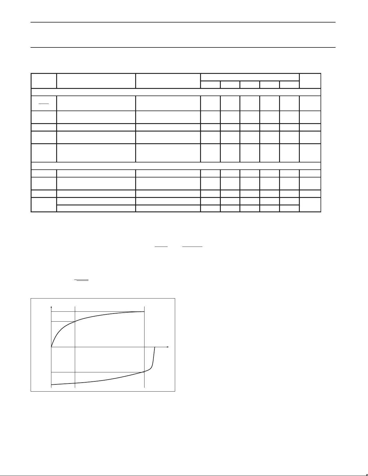
AC ELECTRICAL CHARACTERISTICS (Continued)
LIMITS
MIN –3σ TYP +3σ MAX
IF Synthesizer (cont.)
DI
CP
I
∆I
CP_M
|I
CP_L
t
t
OFF
Serial Interface
f
CLOCK
t
NOTES:
1. Parameter measured relative to modulation sideband amplitude.
2. After programming the DC offset register for minimum offset. DCRES = 562kΩ.
3. The turn on time relates only to the power up time of the circuit. The settling time of the integrated baseband filters has to be added (for
GSM–mode = 8µs with filter bandwidth setting resistor = 36kΩ).
4. The relative output current variation is defined thus:
5. The output current matching is measured when both (positive current and negative current) sections of the output charge pumps are on.
6. As soon as P
7. Guaranteed by design.
8. NF =
9. Minimium frequency is guaranteed by design.
Relative output current variation
CP
Output current matching
| Output leakage current VCP = 0.3V to VCCCP-0.3V -0.02 0.1 0.22 ±15 nA
Turn ON time
ON
Turn OFF time
7
Clock frequency 10 MHz
Set-up time: DATA to CLOCK,
SU
CLOCK to STROBE
t
Hold time: CLOCK to DATA 30 ns
H
Pulse width: CLOCK 30
W
Pulse width: STROBE 30
ON
ǒ
20log
ƪ
CURRENT
I
2
I
1
I
2
I
1
Figure 3. Relative Output Current Variation
6
PLL is set to LO, the phase detector is reset and no charge pumps pulses are generated.
E
no
Ǔ
* VG
ƫ
Ǹ
4kTR
V
1
FUNCTIONAL DESCRIPTION
Serial Programming Input
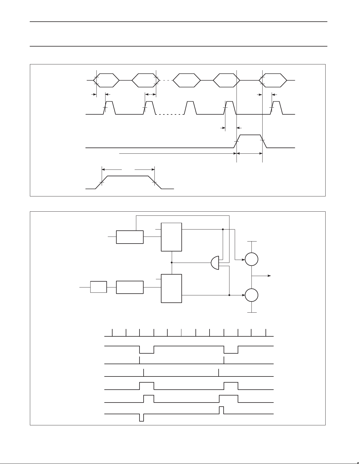
The serial input is a 3-wire input (CLOCK, STROBE, DATA) to
program the counter ratios, charge pump current, status- and
DC-offset register, mode select and test register. The programming
data is structured into two 21-bit words; each word includes 4 chip
5
where, E
4
I
=31.2µA 0.1 1.3 2.5 ±10 %
REF
I
=31.2µA,
REF
VCP = VCCCP/2
POnPLL = HI, to full charge
pump current
POnPLL = LO, to ICCCP,
ICCDIG <5% of operational
supply current
DI
OUT
I
is the output noise voltage measured in a 1Hz bandwidth, R = 1200Ω, VG = gain in dB.
no
VOLTAGE
V
2
SR00526
+ 2@
±12 %
15 µs
15 µs
30 ns
(I
* I1)
2
|(I
; with V1 = 0.3V, V2 = VCCCP – 0.3V (see Figure 3).
) I1)|
2
address bits and 1 subaddress bit. Figure 2 shows the timing
diagram of the serial input. When the STROBE = L, the clock driver
is enabled and on the positive edges of the CLOCK the signal on
DATA input is clocked into a shift register. When the STROBE = H,
the clock is disabled and the data in the shift register remains stable.
Depending on the value of the subaddress bit the data is latched
into different working registers. Table 3 shows the contents of each
word.
Default States
Upon power up (VCCDIG is applied) a reset signal is generated,
which sets all registers to a default state. The logic level at the
STROBE pin should be low during power up to guarantee a proper
reset. These default states are shown in Table 3.
Reference Divider
The reference divider can be programmed to four different division
ratios (:13, :26, :39, :52), see registers r0, r1; default setting: divide
by 13.
Main Divider
The external VCO signal, applied to the LOIN and LOINX inputs, is
divided by two and then fed to the main divider (:N). The main
divider is a programmable 9 bit divider, the minimum division ratio is
1997 Sept 03
8
Page 9
Philips Semiconductors Product specification
m
x0
x1
yg
SA1638Low voltage IF I/Q transceiver
divide by 64. The division ratio is binary coded and set in the
registers n0 to n8. The default setting is a divide by 400.
At the completion of a main divider cycle, a main divider output is
generated which will drive the phase detector.
Phase Detector
The phase detector is a D-type flip-flop phase and frequency
detector shown in Figure 5. The flip-flops are set by the negative
edges of the output signals of the dividers. The rising edge of the
signal L will reset the flip-flops after both flip-flops have been set.
Around zero phase error this has the effect of delaying the reset for
1 reference input cycle. This avoids non-linearity or deadband
around zero phase error. The flip-flops drive on-chip charge pumps.
A source current from the charge pump acts to increase the VCO
frequency; a sink current acts to decrease the VCO frequency.
Current Setting
The charge pump current is defined by the current set between the
pin I
and VEECP. The current value to be set there is 31.2µA.
REF
This current can be set by an external resistor to be connected
between the pin I
setting resistor) can be calculated with the formula
R
The current can be set to zero by connecting the pin I
and VEECP. The typical value R
REF
V
CP 1.4V
CC
EXT
31.2
A
(current
EXT
to VCCCP.
REF
Charge Pumps
The charge pumps at pin CP are driven by the phase dectector and
the current value is determined by the binary value of the charge
pumps register CN = c2, c1, c0, default 1mA. The active charge
pump current is typically:
|I
| (c0 2c1 4c2) 71mA 500mA
CP
Lock Detect
The output LOCK is H when the phase detector indicates a lock
condition. This condition is defined as a phase difference of less
than ±1 cycle on the reference input CLK
, CLKINX.
IN
Test Modes (Synthesizer, Transmit Mixer)
The LOCK output is selectable as a test output. Bits x0, x1 control
the selection, the default setting is normal lock output as described
in the Lock detect section. The selection of a Bit x0, x1 combination
has a twofold effect: First it routes a divider output signal to the
LOCK pin, second it disables mixer stages in the transmit path.
Setting x0,1 = 11 disables both transmit path mixers. This mode can
be used to prevent the transmitter from producing an IF output
signal even if the transmit part is powered on (PDTx = 0V). This can
be used to simplify the control timing while commanding the transmit
and receive simultaneously without the transmit part causing
interference.
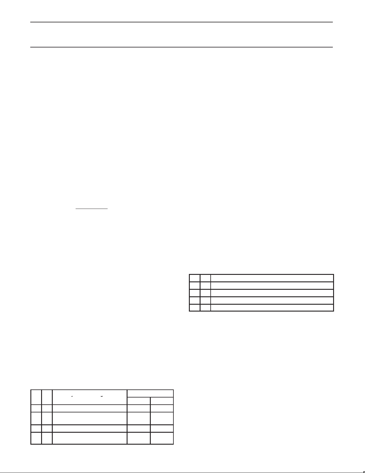
Table 1. Test Modes
Synthesizer Signal
at LOCK Pin
0 0 normal lock detect on on
1 0
0 1 LOIN ÷ 2 * (main divider ratio) on off
1 1
CLKIN divided by reference
divider ratio
main divider output, that goes to
the phase detector
Transmit Mixer
Q-mixer I-mixer
off on
off off
Status Register
The s0 and s1 status bits determine the values of the logic output
pins A
control inputs A and B of the SA1620. (See Figure 9)
OUT
and B
. These outputs can be connected to the AGC
OUT
DC Offset Register
Registers i0 to i3 and q0 to q3 control a correction to the output DC
offset of the I and Q channels of the receiver. The polarity of the DC
offset correction in the I and Q channels are determined by i0 and
q0, respectively. The other bits set the magnitude of the offset
correction. The step size of the two offset correction DACs is fixed
by an external resistor between the DCRES pin and ground. A
value of 120kΩ will give a step size of 200mV.
Mode Select Register
t0: switches the RX IF gain.
t0 = 0 no attenuation
t0 = 1 10dB attenuation
The attenuation switch is included between the IF amplifier and the I
and Q mixers, thereby influencing the noise figure negligibly. The
purpose of this switch is to provide another AGC step which does
not influence the receiver noise figure. Please note that this gain
change will influence the DC offset of the I and Q mixers.
t1 = 0 test mode only, always to be set to 0.
t2, t3 sets the mode of the level locked loop (LLL)
The LLL is a circuit which processes the LO input signal in order to
provide an LO signal with a perfect 50% duty cycle, which
determines the precision of the 90° shift of the I and Q mixing
signals generated by the ÷2 divider. For an external tuning of the
90° phase shift of the I and Q mixing signals, a trimming resistor
may be connected (but is not required) between the ADJ
ground, and the LLL has to be put in one of the following modes:
pin and
IN
Table 2. Mode Select Register
t2 t3 LLL Status
0 0 LLL on (no external tune, monitor performance, default)
0 1 LLL on (with medium external tune)
1 0 LLL off (tune externally)
1 1 LLL on (with fine external tune)
t4 selects the bandwidth of the RC low pass filters at the I, Q
Rx mixer outputs
t4 = 0 cutt-off frequency (-3dB) 110kHz
t4 = 1 cutt-off frequency (-3dB) 792kHz
t5 selects the bandwidth of the integrated 5th-order gyrator
filters. The filters are tuneable over a range of 50kHz to
1MHz with external resistors. The -3dB bandwidth is
inversely proportional to the value of the external resistor.
With
t5, two external resistor values are selectable.
t5 = 0 the resistance between the pins RESA and
RESB determines the cutoff frequency . For
GSM a nominal bandwidth of 80kHz is chosen
when the external resistor is 36kΩ.
t5 = 1 a second resistor between the pins RESB and
RESD is connected in parallel to the first
external resistor, thus increasing the filter
bandwidth. The relative amplification is
decreased in this mode.
1997 Sept 03
9
Page 10
Philips Semiconductors Product specification
Address SA1638
Mode Select Register
SA1638Low voltage IF I/Q transceiver
P
The overall filter response in the receive section is the sum of the
filter responses of the passive RC low-pass filter and the active
gyrator filter.
Power Down Modes
There are 4 power-on pins in the SA1638: PON, PONRx, PDTx,
PLL.
P
ON
P
= H powers up both voltage regulators V
ON
REG
1 and V
REG
2. P
ON
should be set to L, if these internal voltage regulators are not to be
used.
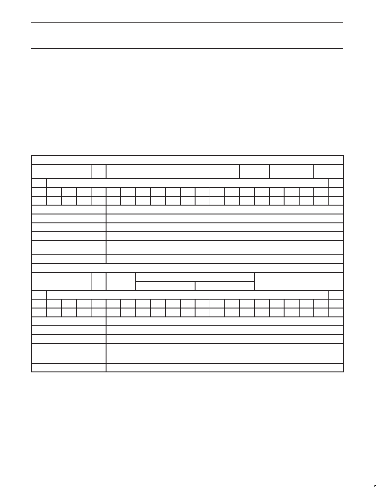
Table 3. Definition of SA1638 Serial Registers
First data word: (shown with default values)
Address SA1638
MSB LSB
a0 a1 a2 a3 sa n0 n1 n2 n3 n4 n5 n6 n7 n8 r0 r1 c0 c1 c2 x0 x1
1 1 1 0 0 1 1 0 0 1 0 0 0 0 0 0 1 1 1 0 0
Sub:Address: 1 bit, sa, fixed to 0 for first data word
Reference Divider Register: 2 bits, r0...r1, 00 = ÷13, 01 = ÷26, 10 = ÷39, 11 = ÷52. Default: 00
Charge-Pump Register: 3 bits, c0...c2, Binary current setting factor for charge pumps, values 000 = minimum current to 111 =
Test Register: 2 bits, x0...x1, default 00, see Functional Description
Second data word: (shown with default values)
MSB LSB
a0 a1 a2 a3 sa s0 s1 q0 q1 q2 q3 i0 i1 i2 i3 t0 t1 t2 t3 t4 t5
1 1 1 0 1 1 1 0 0 0 0 0 0 0 0 0 0 0 0 0 0
Sub:Address: 1 bit, sa, fixed to 1 for second data word
Status Register: 2 bits, s0 sets pin A
DC Offset Register: 4 bits per channel, i0...i3 and q0...q3, no correction as default
Mode Select Register: 6 bits, t0...t5, 000000 = normal GSM-Operation as default, see Functional Description
Sub
Adr
N-Divider Ref ÷ Reg Charge-Pump Reg Test
Address: 4 bits, a0...a3, fixed to 1110
N-Divider: 9 bits, n0...n8, values 64 (00100 0000) to 511 (111111111) allowed for IF-choice, default 400
maximum current, default maximum charge pump current
Sub Status
Adr Reg
Q-Channel I-Channel
DC Offset Register
Address: 4 bits, a0...a3, fixed to 1110
; s1 sets pin B
OUT
i0 and q0 switches offset polarity, 0 to lower voltage, 1 to higher voltage
il...i3 and q1...q3, 000 no correction to 111 max. correction enabled
Rx = H powers up the receiver part.
ON
PDTx = L powers up the transmitter part.
PONPLL = H powers up the synthesizer part. As it also powers up
the first divide by 2 stage for generating the 0/90 degree phase
shifted signals for the transmit and receive mixers, it also has to be
set H if either the transmit part or the receive part is used. P
= L powers down the dividers, resets the phase detector and
disconnects the current setting pin I
. In PONPLL = L mode, the
REF
values in the serial input registers are still kept and the part still can
be reprogrammed as long as V
, see Functional Description
OUT
DIG is present.
CC
ON
PLL
1997 Sept 03
10
Page 11
Philips Semiconductors Product specification
SA1638Low voltage IF I/Q transceiver
LSB MSB
DATA
X1 or t
t
SU
5
X0 or t
4
t
H
a
1
a
0
t
SU
STROBE
LO
CLOCK
STROBE
CLOCK
IN
CLK
50%
÷2
FIRST CLOCKLAST CLOCKFIRST CLOCK
t
SU
50%
CLOCK ENABLED
SHIFT IN DATA
t
W
CLOCK
DISABLED
STORE DATA
SR00527
Figure 4. Serial Input Timing Sequence
L
“1”
D
Q
IN
REFERENCE
DIVIDER
MAIN
DIVIDER
C
R
R
“1”
X
R
D
C
Q
VCCCP
P
N
P-TYPE
CHARGE PUMP
C
P
N-TYPE
CHARGE PUMP
1997 Sept 03
CLK
V
SS
IN
L
R
X
P
N
I
CP
SR00528
Figure 5. Phase Detector Structure with Timing
11
Page 12
Philips Semiconductors Product specification
SA1638Low voltage IF I/Q transceiver
PIN FUNCTIONS
PIN
No.
47 VCCTxRx 3.0
48 GND
1V
2V
3V
4 GND
5PON3.3
6V
6V
PIN
MNEMONIC
1 0.0
REG
1 3.0
REG
F2 3.0
REG
2 3.0
REG
2 0.0
REG
BATT
BATT
DC V EQUIVALENT CIRCUIT
3.3
3.3
BG
1.2
35k
25k
BG
1.2
35k
25k
2.5
—
+
40 43 46
2.5
—
+
40 43 46
5
6
1
47
48
5
6
3
2
4
PIN
No.
MNEMONIC
10 RES
11 RES
12 RES
PIN
DC V EQUIVALENT CIRCUIT
0.05
D
0.00
A
0.05
B
10
t5
11 40 43 46
12
7A
8B
9DC
OUT
OUT
RES
3.0
3.0
1.6
13 P
7
14 V
8
15 QRX
9
16 QRX
17 IRX
18 IRX
Rx 3.0
ON
REF
OUT
X 1.5
OUT
OUT
X 1.5
OUT
1.5
1.5
1.5
13
14
15, 17 16, 18
SR00529
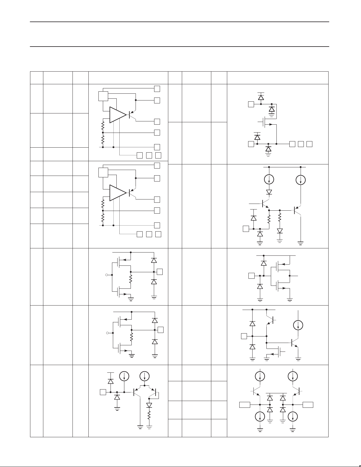
Figure 6. Pin Functions
1997 Sept 03
12
Page 13
Philips Semiconductors Product specification
SA1638Low voltage IF I/Q transceiver
PIN FUNCTIONS (continued)
PIN
No.
PIN
MNEMONIC
DC V EQUIVALENT CIRCUIT
PIN
No.
PIN
MNEMONIC
DC V EQUIVALENT CIRCUIT
QTX
19
QTX
ITX
ITX
IN
23 0.0
PdTx
1.5
IN
X 1.520
IN
1.521
IN
X 1.522
24 3.0VCCDIG
25 3.0VEEDIG
26 DATA
27 CLOCK
28 STROBE
29 LOCK
19, 20, 21, 22
23
26, 27, 28
35 I
REF
1.6
35
36 0.0VEECP
37 CP
38 3.0V
CC
CP
39 3.0PONPLL
39
37
40 0.0GND3
41 42
41 TXIF
29
OUT
X
OPEN
COLLECTOR
30 CLK
31 CLK
32 ADJ
33 2.0LO
34 2.0LOINX
1997 Sept 03
IN
X 2.0
IN
IN
IN
2.0
30 31
2.0
32
33 34
42 TXIF
OUT
X
43 0.0GND2
44 RxIFINX
45 RxIF
IN
46 GND1 0.0
47 VCCTxRx 3.0
48 GND
REG
1 0.0
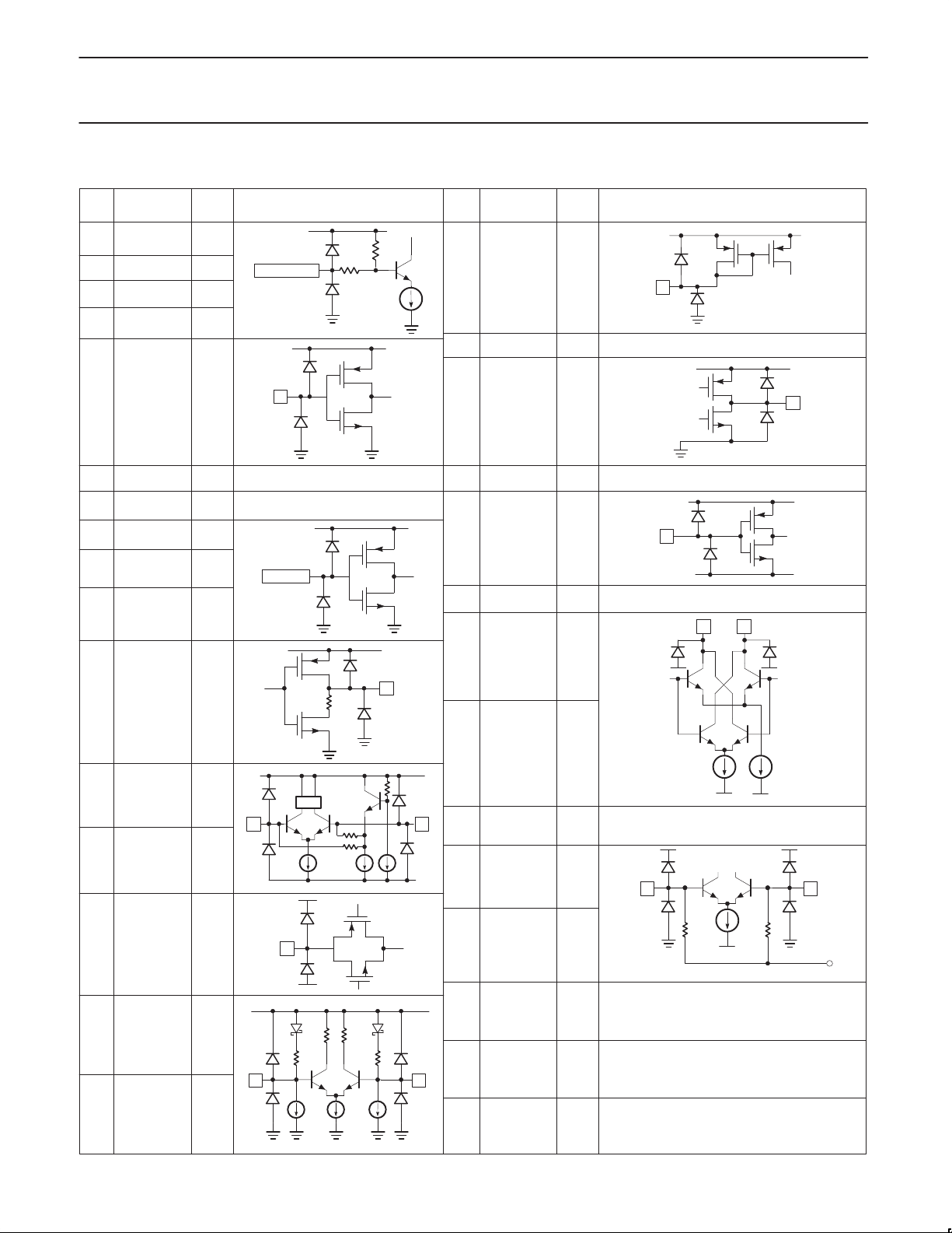
Figure 7. Pin Functions (cont.)
13
OPEN
COLLECTOR
1.5
1.5
44 45
V
REF
SR00530
Page 14

Philips Semiconductors Product specification
SA1638Low voltage IF I/Q transceiver
Overview of Dual GSM/PCN Architecture
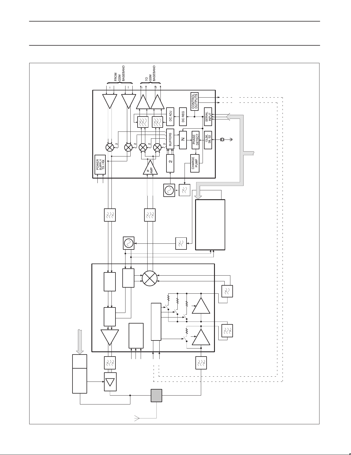
The SA1620 RF front-end and SA1638 IF transceivers form a dual
conversion architecture which uses a common IF and standard I/Q
baseband interface for both transmit and receive paths. The time
division multiplex nature of the GSM system permits integration of
the transmit and receive functions together on the one RF and one
IF chips. This simplifies the distribution of local oscillator signals,
maximizes circuitry commonality, and reduces power consumption.
The SA1620 and SA1638 allow considerable flexibility to optimize
the transceiver design for particular price/size/performance
requirements, through choice of appropriate RF and IF filters. The
IF may be chosen freely in the range 70–400 MHz. The same IF
can be used in the transmit and receive directions. Alternately,
different IFs can be used if the SA1638 synthesizer frequency is
switched between transmit and receive timeslots. The comparison
frequency of the SA1638 PLL is high in order to provide fast
switching time.
With suitable choice of the IF, an identical SA1638 IF receiver
design can be used for both 900MHz GSM and 1800MHz PCN
(DCS1800) equipment.
General Benefits/Advantages
•2.7V operation. Compatible with 3V digital technology and
portable applications. (Higher voltage operation also possible, if
desired.)
•Excellent dynamic range. The availability of two LNAs in the
SA1620 allows flexibility in receiver dynamic design for portable
and mobile GSM spec. applications with appropriate filters. If for
a particular application a GaAs or discrete front-end is desired,
one of the LNAs can be left unpowered. Placing the AGC gain
switches at the front results in some attenuation most of the time,
further increasing typical dynamic performance beyond that
specified by GSM.
•High power transmit output driver, delivering +7.5dBm output.
This is sufficient to drive a filter and power amplifier input, without
a driver amplifier. To avoid unnecessary current consumption, the
output power can be reduced to an appropriate level by choice of
an external resistor.
•DC offsets generated in the receive channel are independent of
the LNA AGC setting, and correctable by software to prevent
erosion of signal handling dynamic range by DC offsets.
•Minimal high-quality filter requirements. As a result of the
integration in the SA1638 of high quality channel selectivity filters,
only sufficient filtering is needed in the receive path to provide
blocking protection for the second mixers. This reduces receiver
cost and size.
•Operation at a high IF allows RF image reject filter requirements
to be relaxed. For example, at a 400MHz IF, the natural gain
roll-off in the SA1620 LNAs and mixer suppresses the image
signal in the 1800MHz band by typically 28dB below the desired
900MHz band signal.
DC Offset Correction
DC offset correction is provided by two DACs each feeding into one
of the two Rx channels. The step size of both DACs is set by the
value of the external resistor between DCRES and ground. Thus
any original offset less than 1.5V magnitude in either channel can be
reduced to the specified level by selecting the appropriate DAC
setting via the serial interface.
Integrated Receive Filters
The low-pass characteristics of the Rx channel are determined by
two low-pass responses. The first of these is a passive filter at the
output of the quadrature mixers and the second is the low-pass
filters which follow the post-mixer amplifiers. These specifications
refer only to the response of the default state, but this may be
switched by the control register to an alternative setting with a
nominal 3dB point of 792kHz.
The corner frequency of the low pass filters can be adjusted over a
wide range by varying the value of the external resistor between
RESA and RESB. The range of feasible corner frequencies extends
at least between 50kHz and 500kHz.
1997 Sept 03
14
Page 15
Philips Semiconductors Product specification
SA1638Low voltage IF I/Q transceiver
P
ON
V
BATT
A
OUT
B
OUT
112kΩ 1MΩ
PONRx
V
REF
10kΩ
0–30mA
0–30mA
100nF
100nF
100nF
1nF
22kΩ
56kΩ
1
2
3
4
5
6
7
8
9
10
11
12
13
14
15
16
VREG1
VREGF2
VREG2
GNDREG2
P
ON
V
BATT
A
OUT
B
OUT
DCRES
RESD
RESA
RESB
P
Rx
ON
V
REF
QRxOUT
QRxOUTX
GNDREG1
TxRx
V
CC
GND1
RxIFIN
RxIFINX
GND2
TxIFOUT
TxIFOUTX
GND3
P
PLL
ON
V
CCP
V
EE
I
REF
LOINX
LOIN
CP
CP
48
47
46
45
33nH
44
43
42
41
40
39
1nF
38
37
36
35
10nF
34
10nF
33
10nF
17.4Ω
294Ω
294Ω
1.8pF
1800Ω
1.8pF
TC4–14
2:1
3V
TC4–14
2:1
100nF
4740Ω
4.7nF
294Ω
17.4Ω
2.5kΩ
51.4Ω
1nF
470pF
51.4Ω
294Ω
PONPLL
800MHz
RxIN
TxOUT
2–3V
V
CCP
VCP
VCO
LOIN
Rx OUT
PD Tx
V
CC DIG
+
–
10kΩ
2.7pF
1997 Sept 03
10kΩ
1nF
10kΩ
I/Q
GEN
DC - 1MHz
1nF 10nF
17
18
19
20
21
22
23
24
IRxOUT
IRxOUTX
QTxIN
QTxINX
ITxIN
ITxINX
PDTx
V
CC DIG
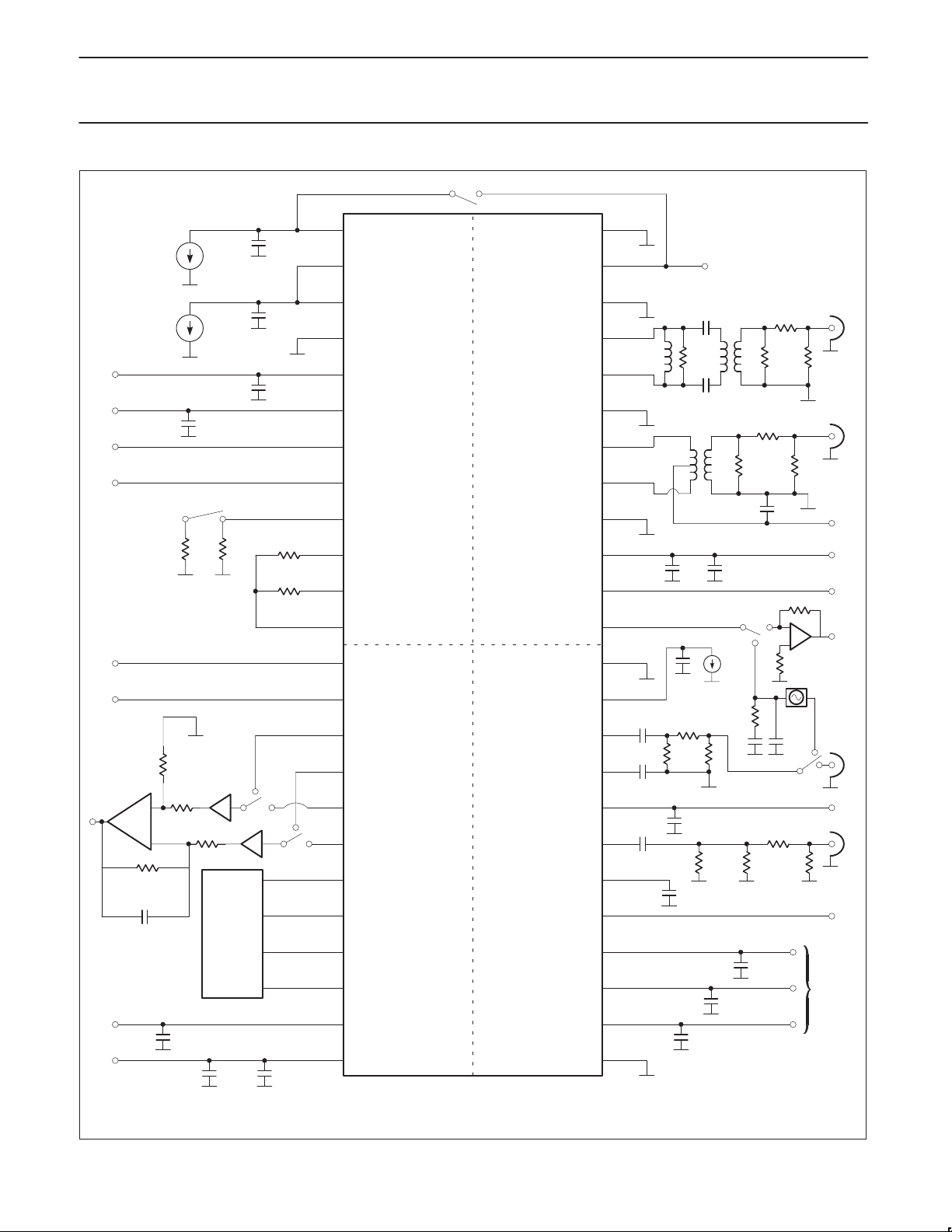
Figure 8. SA1638 Test Circuit
15
ADJ
CLKIN
CLKINX
LOCK
STROBE
CLOCK
DATA
V
EE DIG
294Ω
ADJ
CLKIN
LOCK
3-WIRE
SERIAL
BUS
IN
32
IN
10nF
31
30
29
28
27
26
25
1nF
10nF
10pF
49.9Ω
10pF
10pF
17.4Ω
294Ω
STROBE
CLOCK
DATA
SR00531
Page 16
Philips Semiconductors Product specification
SA1638Low voltage IF I/Q transceiver
I
I
I
Q
I
Q
Q
VAR LPF
Q
BOUT
(to SA1620 ATTENUATION
CONTROL LOGIC INPUTS)
AOUT
SA1638
400MHz
LINEAR
IF LEVEL
CONTROL
400MHz
LO1
(1290–1360MHz)
BUFFER
LO2
800MHz
SAW
÷
÷
PD
÷
CLKIN
13MHz
(SA8025, UMA1019)
FREQUENCY SYNTHESIZER
INTERFACE TO
MICROCONTROLLER
1997 Sept 03
INTERFACE TO
MICROCONTROLLER
SA1620
INPUT
SERIAL
PCA5075
POWER AMP
CONTROLLER
SSB
MIXER
ATTENUATION
A
Tx:
935–960MHz
CONTROL LOGIC
B
Rx:
890–915MHz
Tx/Rx
POWER
SUPPLY
PA
PD
LNA1 LNA2
Figure 9. SA1620 / SA1638 System Block Diagram
16
SR00532
Page 17
Philips Semiconductors Product specification
SA1638Low voltage IF I/Q transceiver
TYPICAL PERFORMANCE CHARACTERISTICS
Regulator Dropout Voltage vs. Temperature and V
5
4.5
4
3.5
3
2.5
VOLTAGE (V)
2
1.5
1
0.5
0
5.5V
3.3V
-50 -40 -30 -20 -10 0 10 20 30 40 50 60 70 80 90
7.5V
Temperature ( °C)
I
LOAD
=30mA
Regulator Powerdown Supply Current vs.
40
Temperature and V
35
7.5V
30
25
µ
5.5V
20
15
CURRENT ( A)
3.3V
10
5
0
-50 -40 -30 -20 -10 0 10 20 30 40 50 60 70 80 90
Temperature ( °C)
BATT
BATT
Regulator Supply Current vs. Temperature and V
7
6.5
6
5.5
5
3.3V
4.5
CURRENT (mA)
5.5V
4
7.5V
3.5
3
-50 -40 -30 -20 -10 0 10 20 30 40 50 60 70 80 90
Temperature (°C)
No Load
Regulator Load Regulation vs.
Temperature and V
1
0.8
0.6
0.4
0.2
-0.2
-0.4
REGULATION (%)
-0.6
-0.8
7.5V
0
5.5V
3.3V
-1
-50 -40 -30 -20 -10 0 10 20 30 40 50 60 70 80 90
Temperature (°C)
BATT
ILoad = 15mA to 30mA
BATT
0.4
0.3
0.2
0.1
0
-0.1
REGULATION (%)
-0.2
-0.3
-0.4
-50 -40 -30 -20 -10 0 10 20 30 40 50 60 70 80 90
1997 Sept 03
Regulator Line Regulation vs.
Temperature and V
Temperature (°C)
BATT
I
LOAD
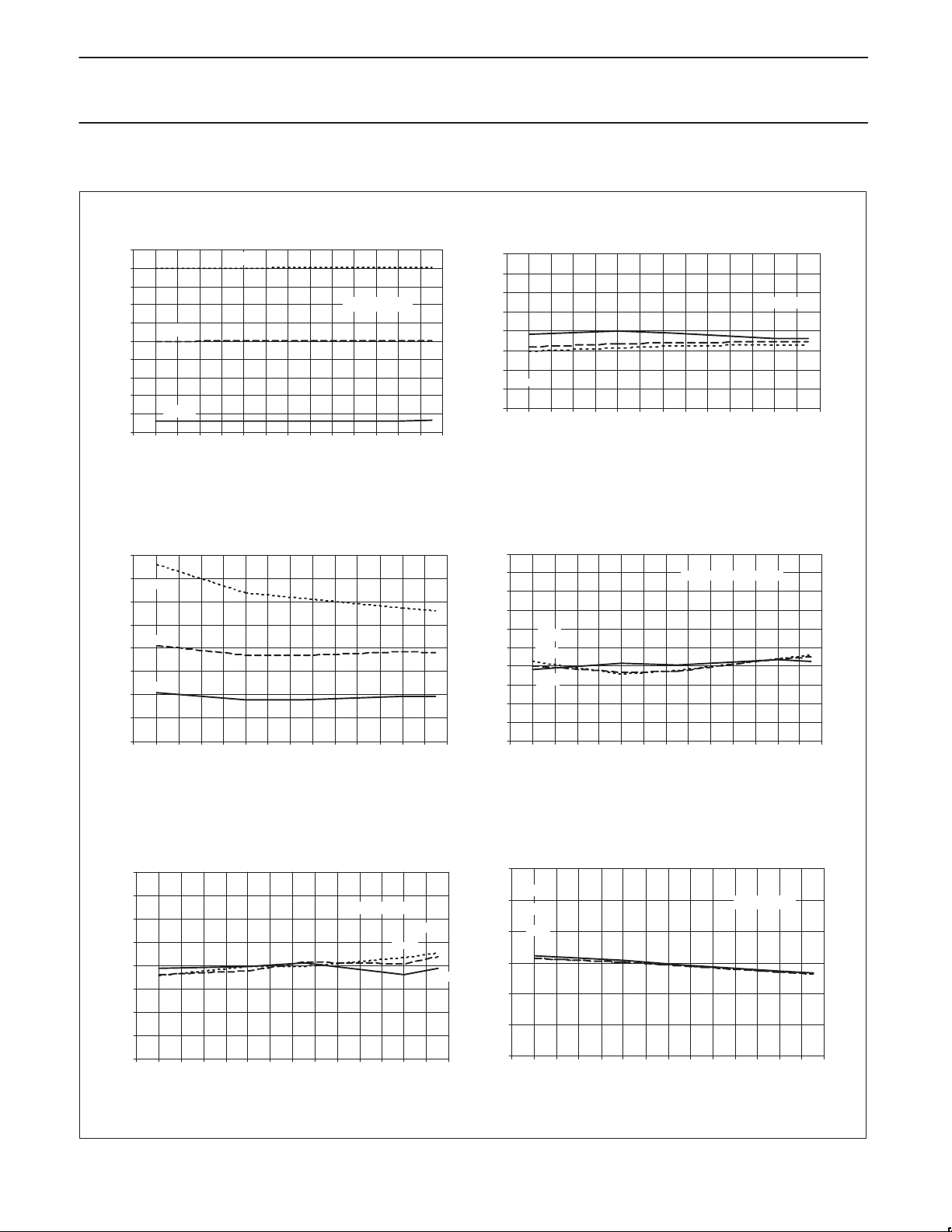
Figure 10. Typical Performance Characteristics
=15mA
5.5V
7.5V
3.3V
Regulator Output Voltage vs.
Temperature and V
3.15
3.3V
3.1
5.5V
7.5V
3.05
3
VOLTAGE (V)
2.95
2.9
2.85
-50 -40 -30 -20 -10 0 10 20 30 40 50 60 70 80 90
Temperature (°C)
BATT
I
17
LOAD
=15ma
Page 18
Philips Semiconductors Product specification
SA1638Low voltage IF I/Q transceiver
TYPICAL PERFORMANCE CHARACTERISTICS (continued)
Transmitter Input Modulation Bandwidth vs.
1100.0
Temperature and V
1050.0
1000.0
950.0
2.7V
900.0
5.5V
4.0V
850.0
FREQUENCY (kHz)
3.0V
800.0
-50 -30 -10 10 30 50 70 90
ITXIN=ITXINX=QTXIN=QTXINX=1.5Vpp
Temperature ( °C)
CC
TxRx
Transmitter Output Third Harmonic vs.
-50
Temperature and V
-55
2.7V
3V
4V
-60
5.5V
-65
DISTORTION LEVEL (dBc)
-70
-50 -30 -10 10 30 50 70 90
Temperature ( °C)
TxRx
CC
TXIN=1.5V
P-P
Transmitter Output Second Harmonic Distortion
-50
Tx In = 1.5V
-55
-60
3V
-65
SECOND HARMONIC LEVEL (dBc)
-70
-50 0 50 100
P-P
4V
5.5V
Temperature ( °C)
Transmitter Output Fourth Harmonic Distortion
-60
Tx In = 1.5V
-65
-70
P-P
2.7V
4V
5.5V
2.7V
3V
-60
-65
-70
FIFTH HARMONIC LEVEL (dBc)
-75
-80
1997 Sept 03
Transmitter Output Fifth Harmonic Distortion
Tx In = 1.5V
-50 0 50 100
P-P
3V
4V
5.5V
Temperature ( °C)
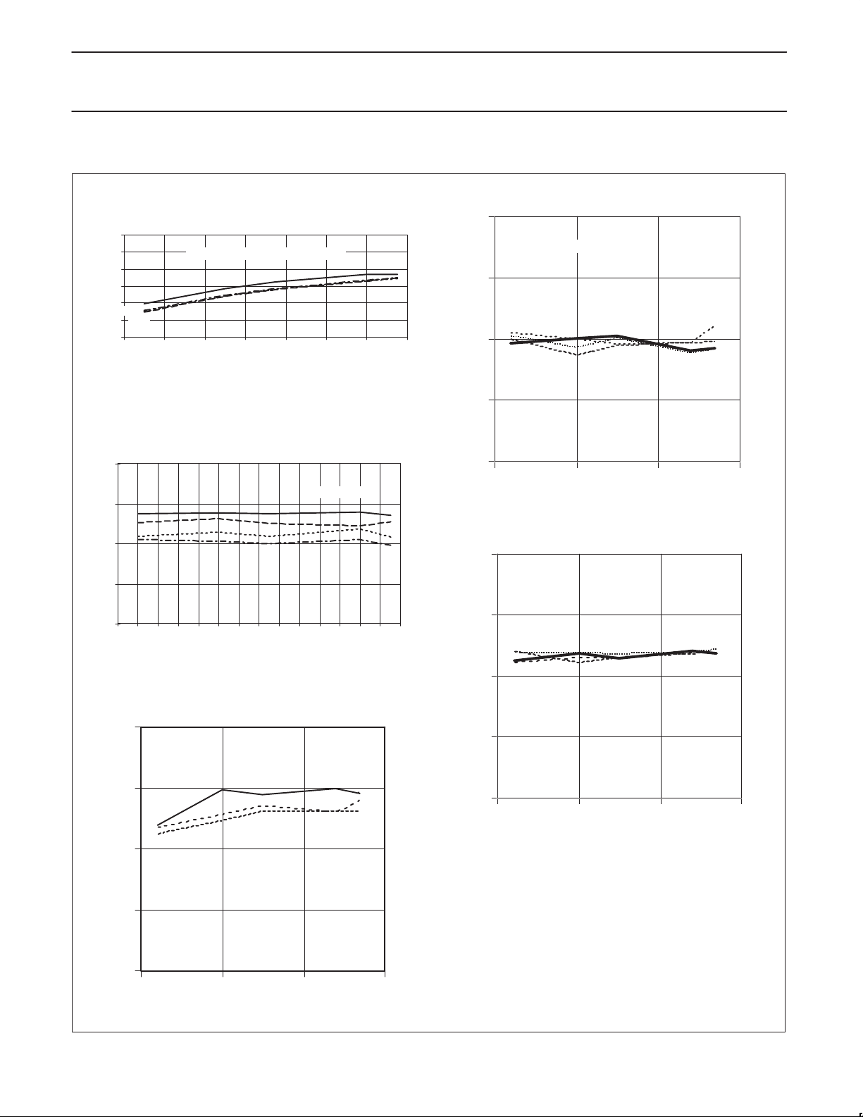
Figure 11. Typical Performance Characteristics (continued)
18
-75
FOURTH HARMONIC LEVEL (dBc)
-80
-50 0 50 100
Temperature (°C)
Page 19
Philips Semiconductors Product specification
SA1638Low voltage IF I/Q transceiver
TYPICAL PERFORMANCE CHARACTERISTICS (continued)
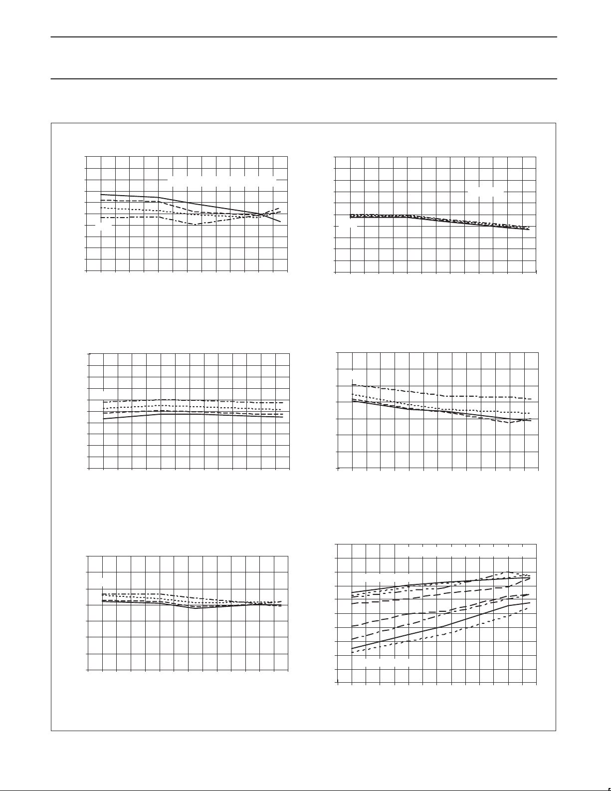
Transmitter Output Saturation vs.
-50
-52
-54
2.7V
-56
3.0V
-58
4.0V
-60
-62
5.5V
-64
-66
-68
-70
5th HARMONIC DISTORTION LEVEL (dBc)
-50 -40 -30 -20 -10 0 10 20 30 40 50 60 70 80 90
Temperature and VccTxRx
TXIFOUT=TXIFOUTX=VccTxRx–0.3V
Temperature ( °C)
Transmitter DC Output Current vs.
2.5
2.4
2.3
2.2
5.5V
2.1
4.0V
2
3.0V
1.9
2.7V
CURRENT (mA)
1.8
1.7
1.6
1.5
-50 -40 -30 -20 -10 0 10 20 30 40 50 60 70 80 90
Temperature and V
Temperature ( °C)
CC
TxRx
Transmitter RMS Output Current
1.1
vs. Temperature and V
1.05
1
0.95
0.9
5.5V
4.0V
0.85
3.0V
0.8
2.7V
0.75
RMS CURRENT (mA)
0.7
0.65
0.6
-50 -40 -30 -20 -10 0 10 20 30 40 50 60 70 80 90
Temperature ( °C)
TxRx
CC
IF=400MHz
Transmitter LO Suppression vs.
Temperature and VccTxRx
-36.0
-38.0
5.5V
-40.0
4.0V
3.0V
-42.0
2.7V
-44.0
SUPPRESSION (dBc)
-46.0
-48.0
-50.0
-50 -40 -30 -20 -10 0 10 20 30 40 50 60 70 80 90
Temperature ( °C)
-35
-40
-45
4.0V
3.0V
-50
2.7V
-55
-60
SUPPRESSION (dBc)
-65
-70
-50 -40 -30 -20 -10 0 10 20 30 40 50 60 70 80 90
1997 Sept 03
Transmitter Side Band Suppresion vs.
V
TxRx and Temperature
CC
5.5V
Temperature ( °C)
Figure 12. Typical Performance Characteristics (continued)
Transmit Noise Floor vs Temperature and Supply Voltage
-126
-127
-128
-129
-130
-131
-132
-133
OUTPUT NOISE (dBc/Hz)
-134
-135
-136
600kHz from Carrier
5.5V
4V
3V
2.7V
5.5V
4V
3V
2.7V
10MHz from Carrier
-50 -40 -30 -20 -10 0 10 20 30 40 50 60 70 80 90
Baseband Input = 1.5V
Temperature (°C)
differential, 30kHz
P-P
19
Page 20
Philips Semiconductors Product specification
SA1638Low voltage IF I/Q transceiver
TYPICAL PERFORMANCE CHARACTERISTICS (continued)
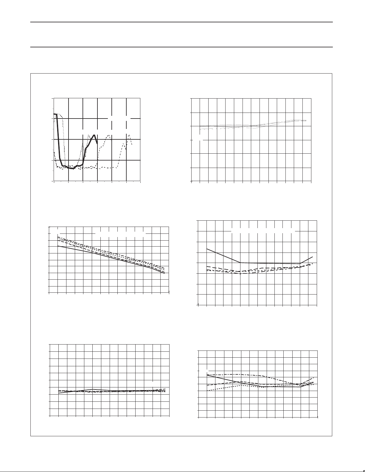
Transmitter Input Common Mode Range
Vs. Supply Voltage
0
4.0V
T = +25°C
5.5V
-20
2.7V
3.0V
-40
5th HARMONIC dBc
-60
-80
0123456
COMMON MODE VOLTAGE
Receiver Gain vs. T emperature and VCCTxRx
60.0
5.5V
58.0
4.0V
56.0
3.0V
54.0
2.7V
52.0
50.0
GAIN (dB)
48.0
46.0
44.0
42.0
40.0
-50 -40 -30 -20 -10 0 10 20 30 40 50 60 70 80 90
IF=400.005MHz, LO=400MHz
Temperature (°C)
Receiver 3dB Bandwidth vs. T emperature and VCCTxRx
100.0
90.0
2.7V
3.0V
80.0
4.0V
5.5V
70.0
FREQUENCY (kHz)
60.0
50.0
40.0
-50 -40 -30 -20 -10 0 10 20 30 40 50 60 70 80 90
Temperature ( °C)
Receiver NF vs T emperature and Supply Voltage
16
14
12
2.7V
10
8
3V
NF (dB)
5.5V
4V
6
4
2
0
-50 -40 -30 -20 -10 0 10 20 30 40 50 60 70 80 90
Relative to 1200Ω source resistance
Temperature (°C)
Receiver Gain match vs VCCTxRx and Temperature
1
0.8
0.6
0.4
0.2
0
3.0V
-0.2
MATCH (dB)
4.0V
-0.4
2.7V
-0.6
-0.8
-1
-50 -40 -30 -20 -10 0 10 20 30 40 50 60 70 80 90
Temperature (°C)
Figure 13. Typical Performance Characteristics (continued)
1997 Sept 03
5.5V
Receiver Channel Matching Phase Error
5
vs. Temperature and V
4
3
2
5.5V
o
1
2.7V
0
ERROR ( )
3.0V
-1
Φ
4.0V
-2
-3
-4
-5
-50 -40 -30 -20 -10 0 10 20 30 40 50 60 70 80 90
Temperature ( °C)
CC
TxRx
20
Page 21
Philips Semiconductors Product specification
SA1638Low voltage IF I/Q transceiver
TYPICAL PERFORMANCE CHARACTERISTICS (continued)
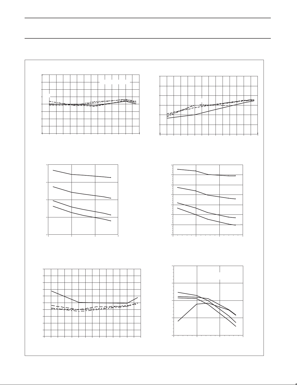
Receiver Corrected Output Offset V oltage
200
vs. Temperature and V
150
100
5.5V
50
4.0V
0
2.7V
3.0V
-50
OFFSET (mV)
-100
-150
-200
-50 -40 -30 -20 -10 0 10 20 30 40 50 60 70 80 90
Temperature (°C)
TxRx
CC
DCRes Resistor=100k
SA1638 Receiver QRXOUT V oltage
1.8
5.5V
1.7
4V
1.6
3V
1.5
PIN 15 DC VOLTAGE (V)
2.7V
Receiver In–band 1dB Compression Point
-47.0
-49.0
-51.0
-53.0
3.0V
4.0V
LEVEL (dBm)
-55.0
2.7V
-57.0
-59.0
-50 -40 -30 -20 -10 0 10 20 30 40 50 60 70 80 90
vs. Temperature and V
5.5V
Temperature ( °C)
CC
TxRx
Reference Voltage
1.8
1.75
1.7
1.65
1.6
VREF (V)
1.55
1.5
5.5V
4V
3V
2.7V
1.4
5.00
4.00
3.00
2.00
1.00
0
IP2 (dBm)
-1.00
-2.00
-3.00
-4.00
-5.00
-50 -40 -30 -20 -10 0 10 20 30 40 50 60 70 80 90
1997 Sept 03
-50 0 50 100
TEMPERATURE (°C)
Receiver IP2 vs T emperature and Supply Voltage
3V
5.5V
4V
2.7V
Temperature (°C)
Figure 14. Typical Performance Characteristics (continued)
21
1.45
-50 0 50 100
TEMPERATURE (°C)
LOIN Maximum Frequency Div800
1100
V
= 100mV
LOIN
1050
3V
1000
FREQUENCY (MHz)
2.7V
950
5.5V
900
-50 0 50 100
TEMPERATURE (°C)
PEAK
4V
Page 22
Philips Semiconductors Product specification
SA1638Low voltage IF I/Q transceiver
TYPICAL PERFORMANCE CHARACTERISTICS (continued)
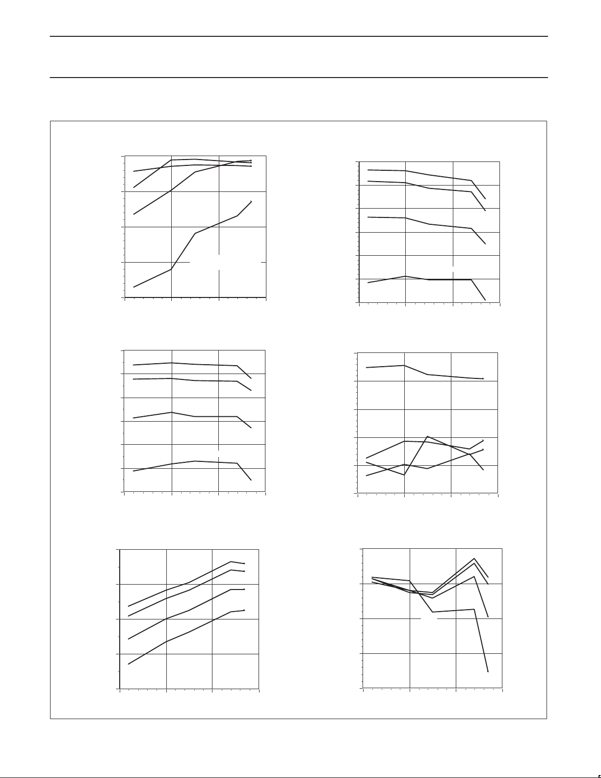
CLKIN Maximum Frequency Div52
250
2.7V
3V
225
4V
200
175
FREQUENCY (MHz)
5.5V
150
-50 0 50 100
V
CLKIN
TEMPERATURE (°C)
P Charge Pump
Output Current 111
-1000
-1010
-1020
µ
-1030
CURRENT ( A)
-1040
-1050
-1060
-50 0 50 100
TEMPERATURE (°C)
= 100mV
5.5V
PEAK
2.7V
4V
N Charge Pump
Output Current 000
-495
2.7V
-500
3V
-505
µ
-510
-515
CURRENT ( A)
-520
-525
-50 0 50 100
TEMPERATURE (°C)
4V
5.5V
N Charge Pump Relative
Output Variation
1.25
5.5V
1
3V
0.75
0.5
VARIATION (%)
4V
0.25
0
-50 0 50 100
3V
2.7V
TEMPERATURE (°C)
1997 Sept 03
Charge Pump Match
-20
-30
µ
-40
CURRENT ( A)
-50
-60
-50 0 50 100
Current 111
5.5V
TEMPERATURE (°C)
Figure 15. Typical Performance Characteristics (continued)
2.7V
3V
4V
22
Charge Pump Output Leakage Current
0.25
0
-0.25
CURRENT (nA)
-0.5
-0.75
-50 0 50 100
5.5V
TEMPERATURE (°C)
2.7V
3V
4V
Page 23
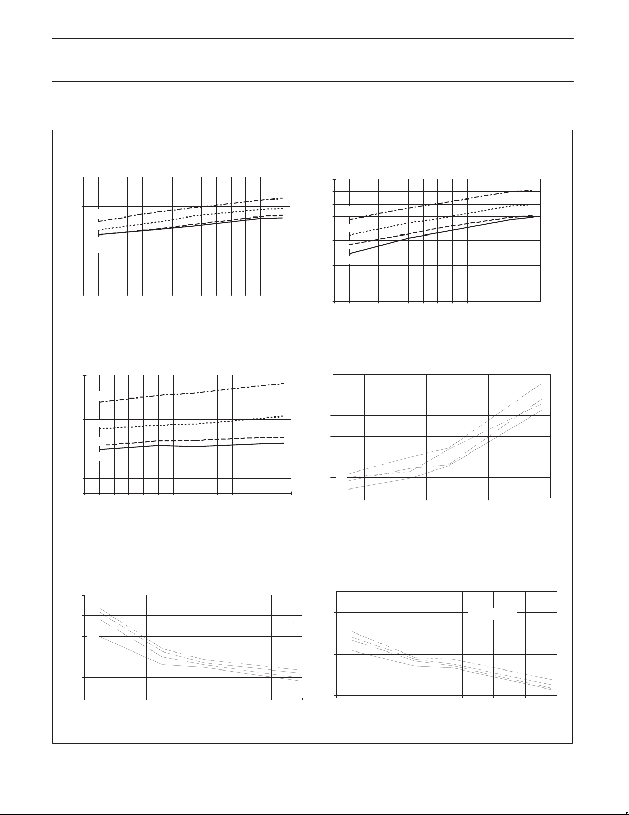
Philips Semiconductors Product specification
SA1638Low voltage IF I/Q transceiver
TYPICAL PERFORMANCE CHARACTERISTICS (continued)
Transmitter Supply Current vs.
26
Temperature and V
24
22
5.5V
20
4.0V
18
3.0V
2.7V
16
CURRENT (mA)
14
12
10
-50 -40 -30 -20 -10 0 10 20 30 40 50 60 70 80 90
Temperature ( °C)
CC
TxRx
Power Down Supply Current vs.
Temperature and V
160
140
5.5V
120
µ
100
4.0V
80
3.0V
60
CURRENT ( A)
2.7V
40
20
0
-50 -40 -30 -20 -10 0 10 20 30 40 50 60 70 80 90
Temperature ( °C)
CC
TxRx
Receiver Supply Current vs.
Temperature and V
20
19
18
5.5V
17
16
4.0V
15
3.0V
14
2.7V
CURRENT (mA)
13
12
11
10
-50 -40 -30 -20 -10 0 10 20 30 40 50 60 70 80 90
Temperature ( °C)
CC
TxRx
Receiver Uncorrected Output Offset
Voltage vs Temperature and V
270
265
260
255
VOLTAGE (mV)
250
5.5V
4.0V
245
3.0V
2.7V
240
-50 -30 -10 10 30 50 70 90
DCRES = 100kΩ
TEMPERATURE (°C)
CC
TxRx
Receiver Output Offset Control Step
Size vs Temperature and V
330
5.5V
4.0V
320
3.0V
310
2.7V
300
VOLTAGE (mV)
290
280
-50 -30 -10 10 30 50 70 90
TEMPERATURE (°C)
TxRx
CC
DCRES = 100kΩ
Figure 16. Typical Performance Characteristics (continued)
1997 Sept 03
Receiver Output Offset Control Step Size vs
37
Temperature and V
36
5.5V
35
4.0V
3.0V
2.7V
34
VOLTAGE (mV)
33
32
-50 -30 -10 10 30 50 70 90
TEMPERATURE (°C)
TxRx
CC
DCRES = 1MΩ
23
Page 24
Philips Semiconductors Product specification
SA1638Low voltage IF I/Q transceiver
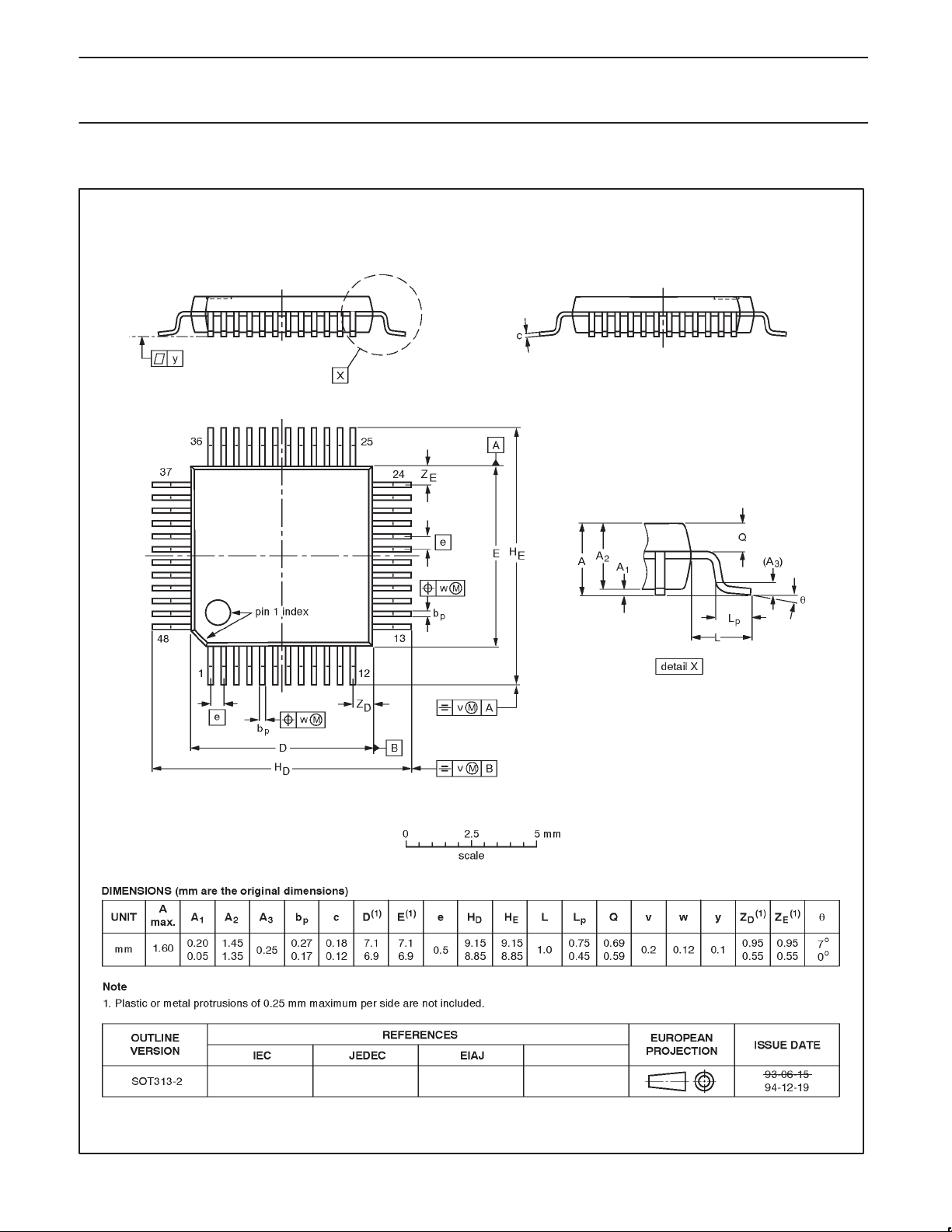
LQFP48: plastic low profile quad flat package; 48 leads; body 7 x 7 x 1.4 mm SOT313-2
1997 Sept 03
24
Page 25

Philips Semiconductors Product specification
SA1638Low voltage IF I/Q transceiver
NOTES
1997 Sept 03
25
Page 26
Philips Semiconductors Product specification
SA1638Low voltage IF I/Q transceiver
Data sheet status
Data sheet
status
Objective
specification
Preliminary
specification
Product
specification
Product
status
Development
Qualification
Production
Definition
This data sheet contains the design target or goal specifications for product development.
Specification may change in any manner without notice.
This data sheet contains preliminary data, and supplementary data will be published at a later date.
Philips Semiconductors reserves the right to make chages at any time without notice in order to
improve design and supply the best possible product.
This data sheet contains final specifications. Philips Semiconductors reserves the right to make
changes at any time without notice in order to improve design and supply the best possible product.
[1]
[1] Please consult the most recently issued datasheet before initiating or completing a design.
Definitions
Short-form specification — The data in a short-form specification is extracted from a full data sheet with the same type number and title. For
detailed information see the relevant data sheet or data handbook.
Limiting values definition — Limiting values given are in accordance with the Absolute Maximum Rating System (IEC 134). Stress above one
or more of the limiting values may cause permanent damage to the device. These are stress ratings only and operation of the device at these or
at any other conditions above those given in the Characteristics sections of the specification is not implied. Exposure to limiting values for extended
periods may affect device reliability.
Application information — Applications that are described herein for any of these products are for illustrative purposes only. Philips
Semiconductors make no representation or warranty that such applications will be suitable for the specified use without further testing or
modification.
Disclaimers
Life support — These products are not designed for use in life support appliances, devices or systems where malfunction of these products can
reasonably be expected to result in personal injury . Philips Semiconductors customers using or selling these products for use in such applications
do so at their own risk and agree to fully indemnify Philips Semiconductors for any damages resulting from such application.
Right to make changes — Philips Semiconductors reserves the right to make changes, without notice, in the products, including circuits, standard
cells, and/or software, described or contained herein in order to improve design and/or performance. Philips Semiconductors assumes no
responsibility or liability for the use of any of these products, conveys no license or title under any patent, copyright, or mask work right to these
products, and makes no representations or warranties that these products are free from patent, copyright, or mask work right infringement, unless
otherwise specified.
Philips Semiconductors
811 East Arques Avenue
P.O. Box 3409
Sunnyvale, California 94088–3409
Telephone 800-234-7381
Copyright Philips Electronics North America Corporation 2000
All rights reserved. Printed in U.S.A.
Date of release: 08-98
Document order number: 9397 750 06847
1997 Sept 03
26
 Loading...