

Page 1
–IN
+IN
EA OUT
GND
REF
SHDN/
FILTER
B OUT
I
SENSE
+V
S
A OUT
1
2
3
4
5
10
9
8
7
6
+
–
R
LIMIT
=
.2
I
LIMIT
R
LIMIT
R
FILTER
C
FILTER
TOP
VIEW
.1µF
C1
PULSE WIDTH MODULATION AMPLIFIER
MICROTECHNOLOGY
HTTP://WWW.APEXMICROTECH.COM (800) 546-APEX (800) 546-2739
FEATURES
• SINGLE SUPPLY OPERATION
• WIDE SUPPLY RANGE — 16-100V
• 20A CONTINUOUS OUTPUT
• PROGRAMMABLE CURRENT LIMIT
• SHUTDOWN CONTROL
• HERMETIC PACKAGE
•2 IN2 FOOTPRINT
APPLICATIONS
• BRUSH TYPE MOTOR CONTROL
• PELTIER CONTROL
• REACTIVE LOADS
• MAGNETIC COILS (MRI)
• ACTIVE MAGNETIC BEARING
• VIBRATION CANCELLING
DESCRIPTION
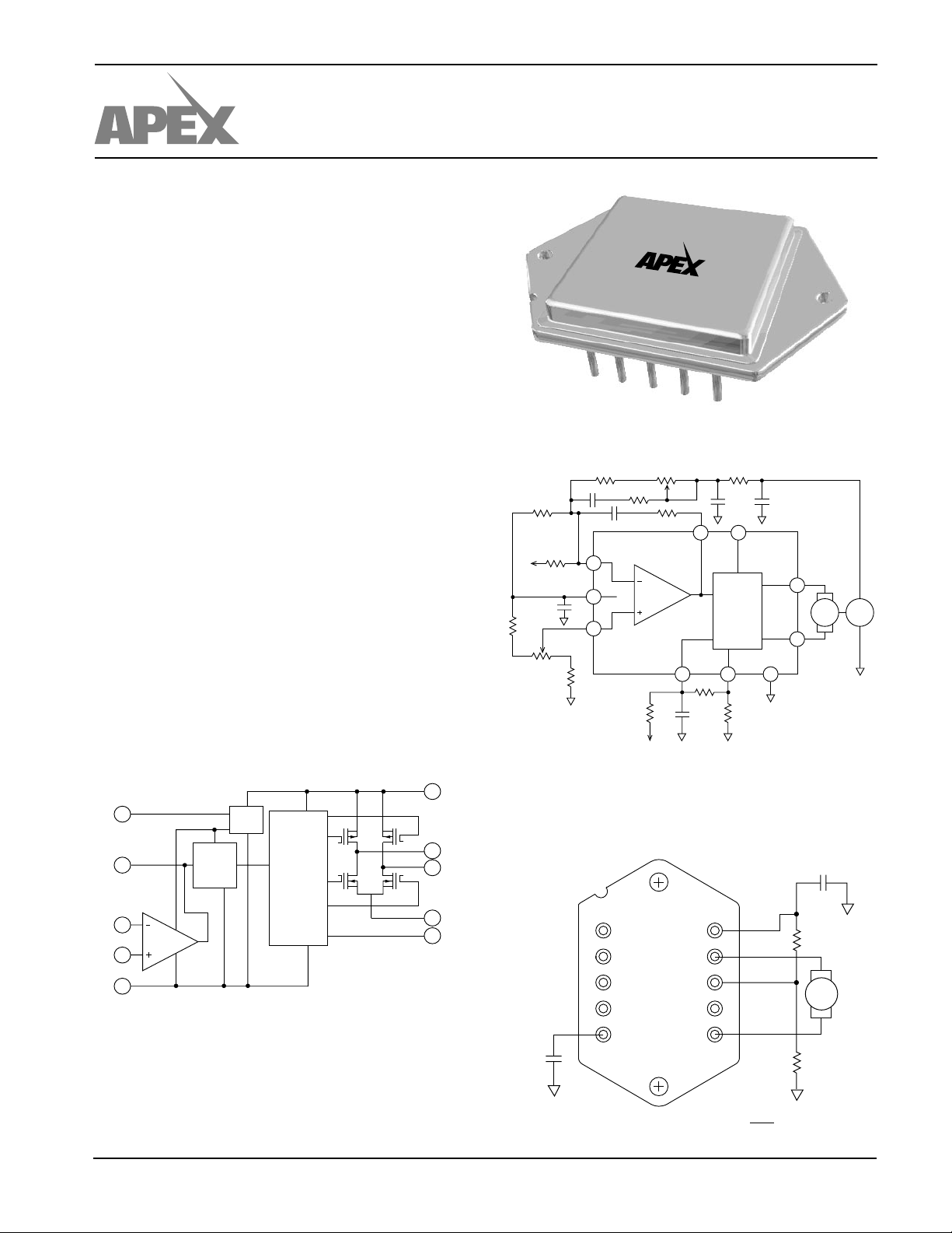
The SA01 amplifier is a pulse width modulation amplifier that
can supply 2KW to the load. The full bridge output amplifier can
be operated from a single power supply over a wide range of
voltages. An error amplifier is included which can provide gain
for the velocity control loop in brush type motor control applications. Current limit is programmable by a single resistor. A
shutdown input turns off all four drivers of the H bridge output.
A precision reference output is provided for use in offsetting
the error amplifier. The error amplifier can then be scaled for
standard input signals. The amplifier is protected from shorts
to supply or ground. The H bridge output MOSFETs are
protected from thermal overloads by directly sensing the
temperature of the die. The 10-pin hermetic power package
occupies only 2 square inches of board space and is isolated.
BLOCK DIAGRAM
+V
10
7
9
6
8
B OUT
A OUT
I
SENSE
SHDN/
FILTER
7.5V REF OUT
5
3
EA OUT
1
–IN
2
+IN
ERROR
AMP
PWM
SUP/
REF
OUTPUT
DRIVERS
CURRENT
LIMIT
AND
SHUTDOWN
CONTROL
SA01
SA01
∆
USA BeO
TE949311
TYPICAL APPLICATION
37
EA
EA
SHDN/
FILTER
OUT
R
C
I
FILTER
FILTER
+V
IN
C1
.1µF
1
5
2
–IN
7.5V
REF
+IN
SA01
SHUT
DOWN
Motor Driver With Tach Feedback
S
EXTERNALCONNECTIONS Package: PD10/60S
SENSE
PWM
R
+V
LIMIT
S
GND
A
OUT
B
OUT
4810
6
MT
9
4
GND
AS EA OUT (3) GOES MORE POSITIVE, HIGH STATE OF A OUT (6)
INCREASES AND HIGH STATE OF B OUT (9) DECREASES.
APEX MICROTECHNOLOGY CORPORATION • TELEPHONE (520) 690-8600 • FAX (520) 888-3329 • ORDERS (520) 690-8601 • EMAIL [email protected]
Page 2

SA01
ABSOLUTE MAXIMUM RATINGS
SPECIFICATIONS
ABSOLUTE MAXIMUM RATINGS
SUPPLY VOLTAGE, +V
OUTPUT CURRENT, peak 30A
S
POWER DISSIPATION, internal 185W
TEMPERATURE, pin solder - 10s 300°C
TEMPERATURE, junction
2
100V
1
150°C
TEMPERATURE, storage –65 to +150°C
OPERATING TEMPERATURE RANGE, case –55 to +125°C
SHUTDOWN VOLTAGE 10V
REFERENCE LOAD CURRENT 10mA
SPECIFICATIONS
PARAMETER TEST CONDITIONS
ERROR AMP INPUT ± 0 to +12V
2
MIN TYP MAX UNITS
ERROR AMP
OFFSET VOLTAGE 10 mV
BIAS CURRENT 5 µA
OFFSET CURRENT 1 µA
COMMON MODE VOLTAGE RANGE
COMMON MODE REJECTION, DC
SLEW RATE 15 V/µS
OPEN LOOP GAIN
4
4
4
+2 +8 V
75 dB
75 dB
GAIN BANDWIDTH PRODUCT 2 MHz
OUTPUT
TOTAL R
EFFICIENCY, 10A OUTPUT VS = 100V 97 %
SWITCHING FREQUENCY 35.3 42 48.7 KHz
CURRENT, continuous
CURRENT, peak
ON
4
4
20 A
30 A
.25 Ω
REFERENCE
VOLTAGE I
VOLTAGE VS. TEMP
OUTPUT CURRENT 5mA
LOAD REGULATION
4
4
= 5mA 7.46 7.50 7.54 V
REF
Full temperature range 50 PPM/°C
20 50 PPM/mA
LINE REGULATION 1 PPM/V
POWER SUPPLY
VOLTAGE Full temperature range 16 50 100 V
CURRENT I
CURRENT, shutdown I
= 0, I
OUT
= 0 25 mA
REF
= 0 76 90 mA
REF
SHUTDOWN
TRIP POINT .18 .22 V
INPUT CURRENT 100 nA
THERMAL
2
RESISTANCE, junction to case Full temp range, for each transistor 1.0 °C/W
RESISTANCE, junction to air Full temperature range 12 °C/W
TEMPERATURE RANGE, case Meets full range specifications –25 +85 °C
NOTES: 1. Each of the two active output transistors can dissipate 125W, however the N-channel will be about 1/3 of the total dissipated
power. Internal connection resistance is .05Ω.
2. Unless otherwise noted: TC = 25°C.
3. Long term operation at the maximum junction temperature will result in reduced product life. Derate internal power dissipation to
achieve high MTTF. For guidance, refer to the heatsink data sheet.
4. Guaranteed but not tested.
CAUTION
The SA01 is constructed from MOSFET transistors. ESD handling procedures must be observed.
The internal substrate contains beryllia (BeO). Do not break the seal. If accidentally broken, do not crush, machine, or
subject to temperatures in excess of 850°C to avoid generating toxic fumes.
APEX MICROTECHNOLOGY CORPORATION • 5980 NORTH SHANNON ROAD • TUCSON, ARIZONA 85741 • USA • APPLICATIONS HOTLINE: 1 (800) 546-2739
Page 3
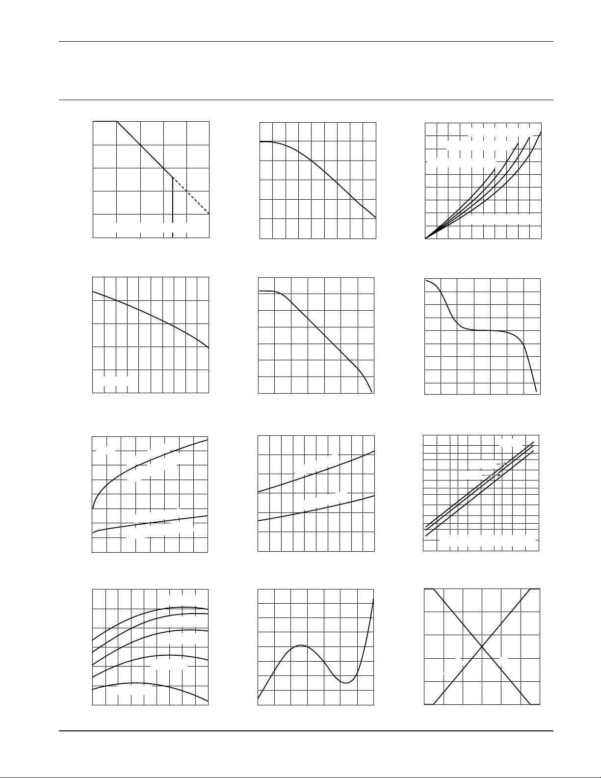
TYPICAL PERFORMANCE
0.1 0.4 1.0 2.0 6.010.0 40.0
0.02
0.06
0.10
0.40
1.00
2.00
6.00
10.0
BRIDGED OUTPUT SWING
VOLTAGE DROP, V
S
– [A
OUT
–B
OUT
] (V)
–55 125
98
100
101
NORMALIZED CLOCK DRIFT
99
0
OUTPUT CURRENT, (A)
VOLTAGE DROP
VOLTAGE DROP, (V)
6
7
8
9
–15 25 85 2 4 6 8 10 12 14 16 18 20
NORMALIZED SWITCHING FREQUENCY, (%)
0
1
2
3
4
5
BRIDGE DRIVE CURRENT, I
OUT
(A)
CASE TEMPERATURE, T (°C)
C
25 125
CASE TEMPERATURE, T
C
(°C)
0
20
25
MAXIMUM CONTINUOUS OUTPUT
OUTPUT CURRENT , (A)
5
10
15
1 10 100 10M
80
120
ERROR AMP SMALL SIGNAL GAIN
40
FREQUENCY, F (Hz)
–180
ERROR AMP SMALL SIGNAL PHASE
45 65 85 105
–55 –50 –25 0 25 50 75 100 125125–15 25 85
1K 10K 100K 1M 1 10 100 10M1K 10K 100K 1M
FREQUENCY, F (Hz)
OPEN LOOP GAIN RESPONSE, A (dB)
–135
–90
–45
0
OPEN LOOP PHASE, (°)ϕ
0
INTERNAL POWER DISSIPATION, P (W)
015
FLYBACK CURRENT, ISD, (A)
0
FLYBACK DIODES
4
5
FET ON RESISTANCE
ON RESISTANCE, (Ω)
POWER DERATING
0
75
125
100
25
50
10 20
1
2
3
0
.05
.1
.15
.2
.25
.3
SOURCE TO DRAIN DIODE VOLTAGE
CASE TEMPERATURE, T (°C)
J
50 110 13070 90 150
75
CASE TEMPERATURE, T (°C)
1000 25 50 125
C
CASE TEMPERATURE, TC (°C) CASE TEMPERATURE, TC (°C)
60
70
80
QUIESCENT CURRENT DRIFT
QUIESCENT CURRENT, IQ (mA)
0.9996
0.9998
1.0000
1.0002
1.0004
NORMALIZED REFERENCE DRIFT
28
CONTROL, EA OUT (V)
0
DUTY CYCLE
PERCENT HIGH
80
4
40
6
NORMALIZED REFERENCE, V
REF
, (X)
125°C
85°C
25°C
A/B OUT TO +V
S
P-CHANNEL
P-CHANNEL
A
OUT
B
OUT
N-CHANNEL
A/B OUT TO I
SENSE
N-CHANNEL
VS = 100V
JUNCTION TEMPERATURE
VS = 80V
VS = 60V
VS = 40V
VS = 20V
TJ = 150°C
25°C
EACH OUTPUT TRANSISTOR
CASE TEMP. 35°C
CASE TEMP. 110°C
CASE TEMP. 60°C
CASE TEMP. 85°C
GRAPHS
SA01
APEX MICROTECHNOLOGY CORPORATION • TELEPHONE (520) 690-8600 • FAX (520) 888-3329 • ORDERS (520) 690-8601 • EMAIL [email protected]
Page 4
SA01
OPERATING
CONSIDERATIONS
GENERAL
Helpful information about power supplies, heatsinking and
mounting can be found in the “General Operating Considerations” section of the Apex data book. For information on the
package outline, heatsinks, and mounting hardware see the
“Package Outlines” and “Accessories” section of the data book.
Also see Application Note 30 on “PWM Basics.”
CURRENT LIMIT
The current limit function sets a peak limit on current flow in
pin 8 (Isense). This limits load current and also limits current in
the event of a short of either output to +Vs. This circuit can trip
anytime during the conduction period and will hold the output
transistors off for the remainder of that conduction period.
For proper operation the current limit sense resistor must be
connected as shown in the external connection diagram. It is
recommended that the resistor be a non-inductive type. Load
current flows in pin 8. No current flows in pin 10 (Shutdown/
filter) so no error will be introduced by the length of the
connection to pin 10. However, the voltage at pin 10 is compared to GND (pin 4) and an error could be introduced if the
grounded end of R
board layout practice would be to connect R
tween pins 8 and 4.
is not directly tied to pin 4. Good circuit
LIMIT
directly be-
LIMIT
Switching noise spikes will invariably be found at pin 8. The
amplitude and duration will be load dependent. The noise
spikes could trip the current limit threshold which is only 200
FILTER
and C
mV. R
switching noise well below 200 mV to prevent false current
should be adjusted so as to reduce the
FILTER
limiting. The sum of the DC level plus the noise peak will
determine the current limiting value. Suggested starting values
are C
= .01µF, R
FILTER
The required value of R
R
where R
maximum desired current.
LIMIT
= .2 V / I
LIMIT
is the required resistor value, and I
FILTER
= 5k.
may be calculated by:
LIMIT
LIMIT
LIMIT
is the
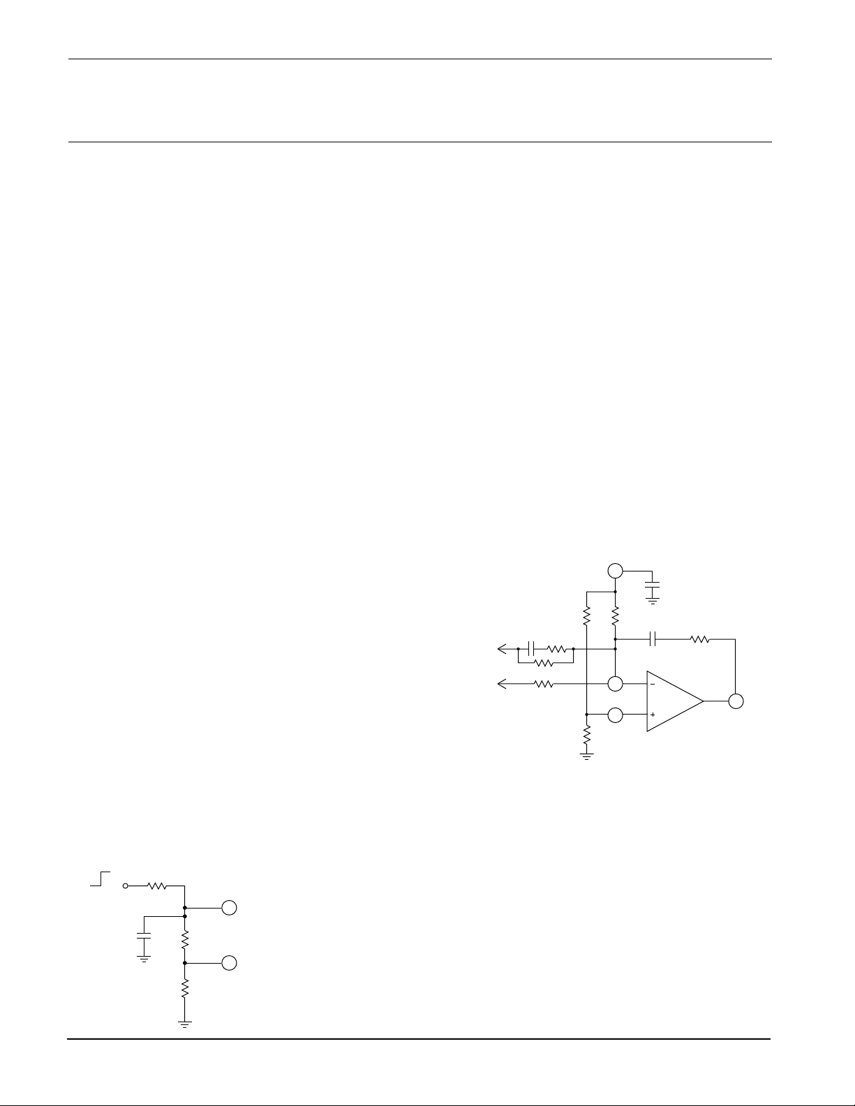
SHUTDOWN
The shutdown circuitry makes use of the internal current
limiting circuitry. The two functions may be externally combined
as shown below in Figure 1. R
value resistor and can be considered zero for this application.
and R
R
SD
After a suitable noise filter is designed for the current limit adjust
the value of R
when the shutdown signal is high. This means pin 10 will reach
form a voltage divider for the shutdown signal.
FILTER
to give 317 mV of shutdown signal at pin 10
SD
the 200 mV trip point in about one time constant with low output
current and less time as output current increases. The voltage
R
SD
LIMIT
SHDN/FILTER
R
FILTER
SHUTDOWN
SIGNAL
C
FILTER
FIGURE 1.
R
will normally be a very low
LIMIT
at pin 10 is referenced
to pin 4 (GND). C
will filter both the cur-
10
rent limit noise spikes
and the shutdown signal. Shutdown and current limit operate on
each cycle of the internal switching rate. As
long as the shutdown
I
SENSE
8
signal is high the output
will be disabled.
FILTER
PROTECTION CIRCUITS
There are two conditions which will latch all the output
transistors off. The first of these conditions is activation of the
high side current limit. Specifically, current in pin 7 (+V
monitored. The DC trip level is about 35A and response time
S
) is
about 5us. As actual currents increase the response time
decreases. The external fault generally associated with this
condition is shorting one of the outputs to ground. However, a
load fault can also activate this high side current limit if the
current rise time is less than the response time of the filter
discussed under “Current Limit”. The second of these conditions is activation of any of the four output transistor overtemperature sensors at about 165°C. Ambient temperature, air
flow, amplifier mounting problems and all the previously mentioned high current faults contribute to junction temperature.
When either of these protection circuits are activated, the root
fault must be corrected and power cycled to restore normal
operation.
DEAD TIME
There is a dead time between the on and off of each output.
The dead time removes the possibility of a momentary conduction path through the upper and lower transistors of each half
bridge output during the switching interval. During the dead
time all output transistors are off. Noise or flyback may be
observed at the outputs during this time due to the high
impedance of the outputs in the off state. This will vary with the
nature of the load.
–IN
+IN
5
R1
1
2
C1
.1µF
R3
3
E/A OUT
TO TACH
SIGNAL
FIGURE 2.
C2
REF OUT
R2
R4
R5
R6
R7
ERROR AMPLIFIER
The internal error amplifier is an operational amplifier. For
highest loop accuracy it is best to configure the op amp as an
integrator (See Figure 2). Feedback can be adjusted with
appropriate poles and zeroes to properly compensate the
velocity loop for optimum stability.
The op amp is operated from a single supply voltage generated internally. The non-inverting input of the op amp does not
have a common mode range which includes ground. R2 and R7
are used with the reference voltage provided at pin 5 to bias the
non-inverting input to +5 volts, which is approximately half of
the voltage supplied internally to the op amp. Similarly, R1 and
the parallel combination of R5 R6 are selected to bias the
inverting input also at +5 volts. Resistors R1 R2 must be
matched. Likewise the parallel combination of R5 R6 must be
matched with R7. The source impedances of the tach and the
signal source may affect the matching and should be considered in the design.
This data sheet has been carefully checked and is believed to be reliable, however, no responsibility is assumed for possible inaccuracies or omissions. All specifications are subject to change without notice.
SA01U REV. E MARCH 1999 © 1999 Apex Microtechnology Corp.
 Loading...