

Datasheet S93VP662S-2.7TE13, S93VP662S-2.7TE7, S93VP662S-ATE13, S93VP662S-ATE7, S93VP662S-BTE13 Datasheet (SUMMIT)
...Page 1
SUMMIT MICROELECTRONICS, Inc. • 300 Orchard City Drive, Suite 131 • Campbell, CA 95008 • Telephone 408-378-6461 • Fax 408-378-6586 • www.summitmicro.com
1
S93VP662/S93VP663
© SUMMIT MICROELECTRONICS, Inc. 1998
2019 1.1 5/15/98
Characteristics subject to change without notice
SUMMIT
MICROELECTRONICS, Inc.
FEATURES
• Voltage Protection™
• Precision Low-VCC Write Lockout
• All Write Operations Inhibited When VCC Falls
below V
LOCK
• One 3Volt and Two 5Volt System Versions
–V
LOCK
= 2.6V+.1V/-.05V
–V
LOCK
= 4.25V +.25V/-0.0V
–V
LOCK
= 4.50 +.25V/-0.0V
• 100% Compatible with Industry Standard
Microwire Devices
• 1,000,000 Program/Erase Cycles
• 100 Year Data Retention
• Commercial Industrial Temperature Range
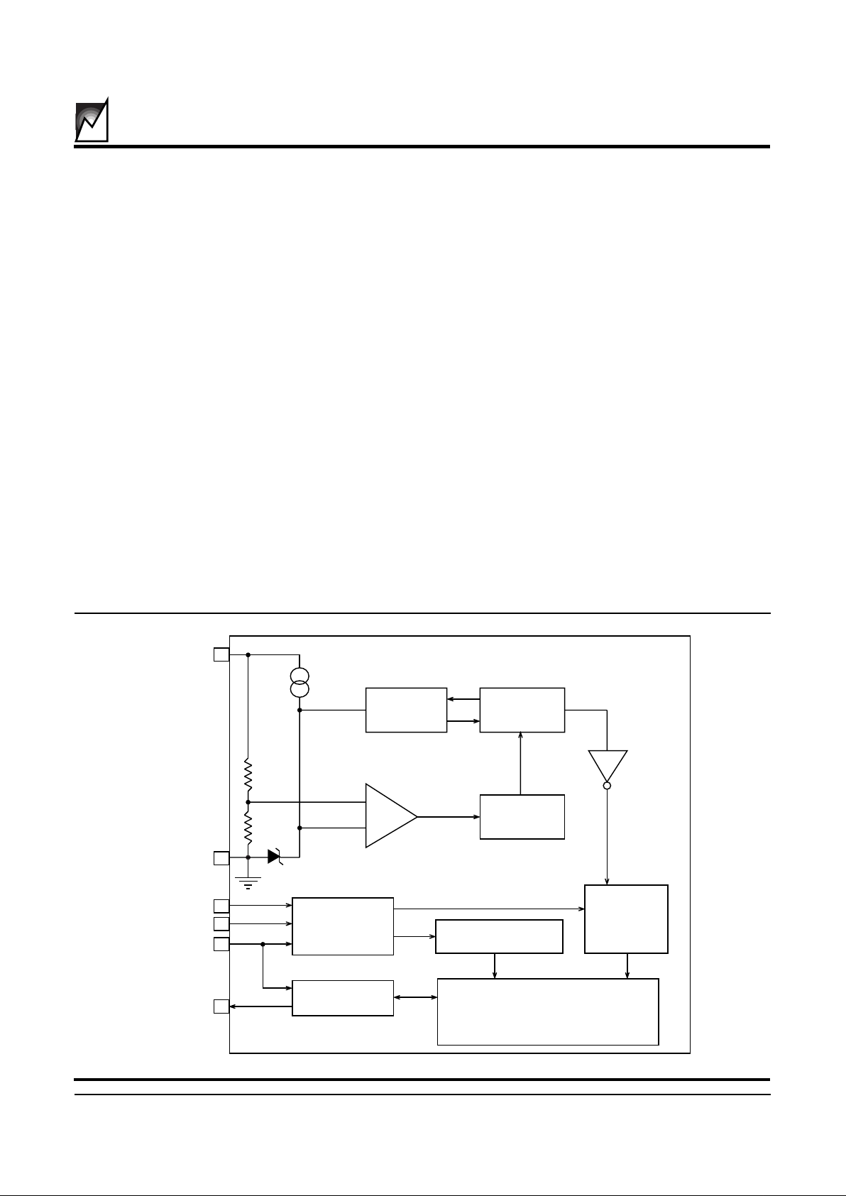
OVERVIEW
The S93VP662 and S93VP663 are 4K-bit serial
E2PROM memories integrated with a precision V
CC
sense circuit. The sense circuit will disable write operations whenever VCC falls below the V
LOCK
voltage. They
are fabricated using SUMMIT’s advanced CMOS
E2PROM technology and is suitable for both 3 and 5 volt
systems.
Both devices have 4k-bits of E2PROM memory that is
accessible via the industry standard microwire bus. The
S93VP662 is configured with an internal ORG pin tied
low providing an 8-bit byte organization and the
S93VP663 is configured with an internal ORG pin tied
high providing a 16-bit word organization. Both the
S93VP662 and S93VP663 have page write capability.
The devices are designed for a minimum 1,000,000
program/erase cycles and have data retention in excess of 100 years.
BLOCK DIAGRAM
4K Serial E2PROM with a Precision Low-VCC Lockout Circuit
+
-
8
CS
DI
DO
SK
1
2
3
4
5GND
2019 ILL2 1.0
MEMORY
ARRAY
4K-Bit
E2PROM
WRITE
CONTROL
ADDRESS
DECODER
MODE
DECODE
DATA I/O
RESET
CONTROL
RESET
PULSE
GENERATOR
5KHz
Oscillator
V
TRIP
1.26V
V
CC
Page 2
2
S93VP662/S93VP663
2019 1.1 5/15/98
PIN FUNCTIONS
Pin Name Function
CS Chip Select
SK Clock Input
DI Serial Data Input
DO Serial Data Output
V
CC
+2.7 to 6.0V Power Supply
GND Ground
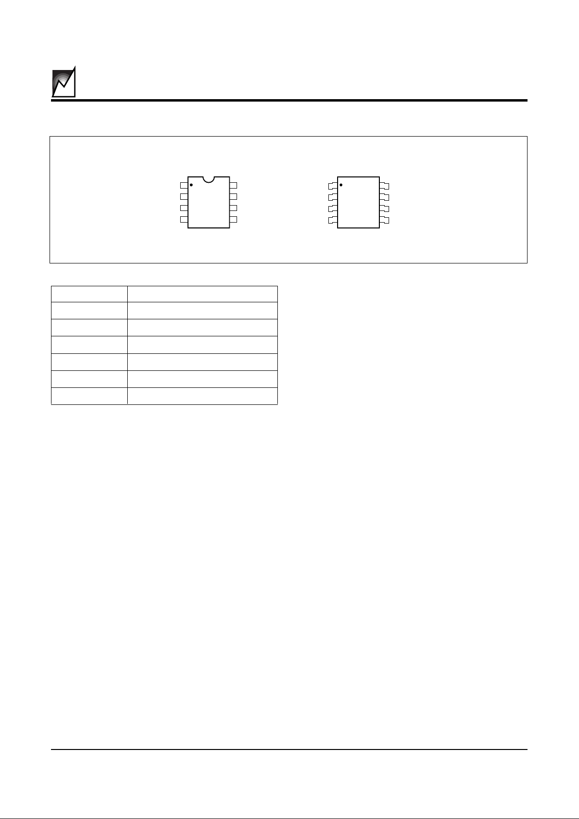
PIN CONFIGURATION
DIP Package (P)
SOIC Package (S)
DEVICE OPERATION
APPLICATIONS
The S93VP662/VP663 was designed specifically for
applications where the integrity of the stored data is
paramount. In recent years, as the operating voltage
range of serial E2PROMs has widened, most semiconductor manufacturers have arbitrarily eliminated their
V
CC
sense circuits. The S93VP662/VP663 will protect
your data by guaranteeing write lockout below the selected VCC Lockout voltage.
VCC Lockout
The S93VP662/VP663 has an on-board precision V
CC
sense circuit. Whenever VCC is below V
LOCK
, the
S93VP662/VP663 will disable the internal write circuitry.
The VCC lockout circuit will ensure a higher level of data
integrity than can be expected from industry standard
devices that have either a very loose specification or no
VCC lockout specification.
During a power-on sequence all writes will be inhibited
below the V
LOCK
level and will continue to be held in a
write inhibit state for approximately 200ms after V
CC
reaches, then stays at or above V
LOCK
. The 200ms delay
provides a buffer space for the microcontroller to complete its power-on initialization routines (reading is OK)
while still protecting against inadvertent writes.
During a power-down sequence initiation of writes will
be inhibited whenever VCC falls below V
LOCK
. This will
guard against the system’s microcontroller performing
an inadvertent write within the ‘danger zone’. (see
AN003)
GENERAL OPERATION
The S93VP662/VP663 is a 4096-bit nonvolatile memory
intended for use with industry standard microprocessors. The S93VP663 is organized as X16, seven 11-bit
instructions control the reading, writing and erase
operations of the device. The S93VP662 is organized as
X8, seven 12-bit instructions control the reading, writing
and erase operations of the device. The device operates
on a single 3V or 5V supply and will generate on chip, the
high voltage required during any write operation.
Instructions, addresses, and write data are clocked into
the DI pin on the rising edge of the clock (SK). The DO
pin is normally in a high impedance state except when
reading data from the device, or when checking the
ready/busy status after a write operation.
The ready/busy status can be determined after the start
of a write operation by selecting the device (CS high) and
polling the DO pin; DO low indicates that the write
operation is not completed, while DO high indicates that
the device is ready for the next instruction. If necessary,
the DO pin may be placed back into a high impedance
2019 ILL1 1.0
CS
SK
DI
DO
V
CC
NC
NC
GND
1
2
3
4
8
7
6
5
CS
SK
DI
DO
V
CC
NC
NC
GND
1
2
3
4
8
7
6
5
Page 3
3
S93VP662/S93VP663
2019 1.1 5/15/98
state during chip select by shifting a dummy “1” into the
DI pin. The DO pin will enter the high impedance state
on the falling edge of the clock (SK). Placing the DO pin
into the high impedance state is recommended in applications where the DI pin and the DO pin are to be tied
together to form a common DI/O pin.
The format for all instructions is: one start bit; two op
code bits and either eight (x16) or nine (x8) address/
instruction bits.
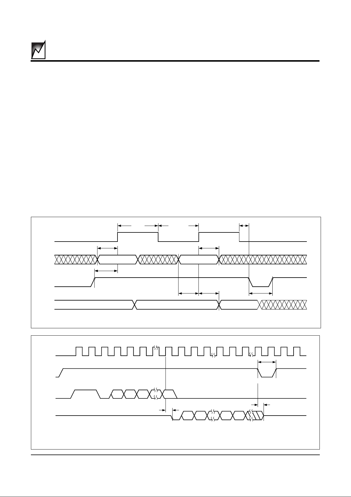
Read
Upon receiving a READ command and an address
(clocked into the DI pin), the DO pin of the S93VP662/
VP663 will come out of the high impedance state and,
will first output an initial dummy zero bit, then begin
shifting out the data addressed (MSB first). The output
data bits will toggle on the rising edge of the SK clock
and are stable after the specified time delay (t
PD0
or
t
PD1
).
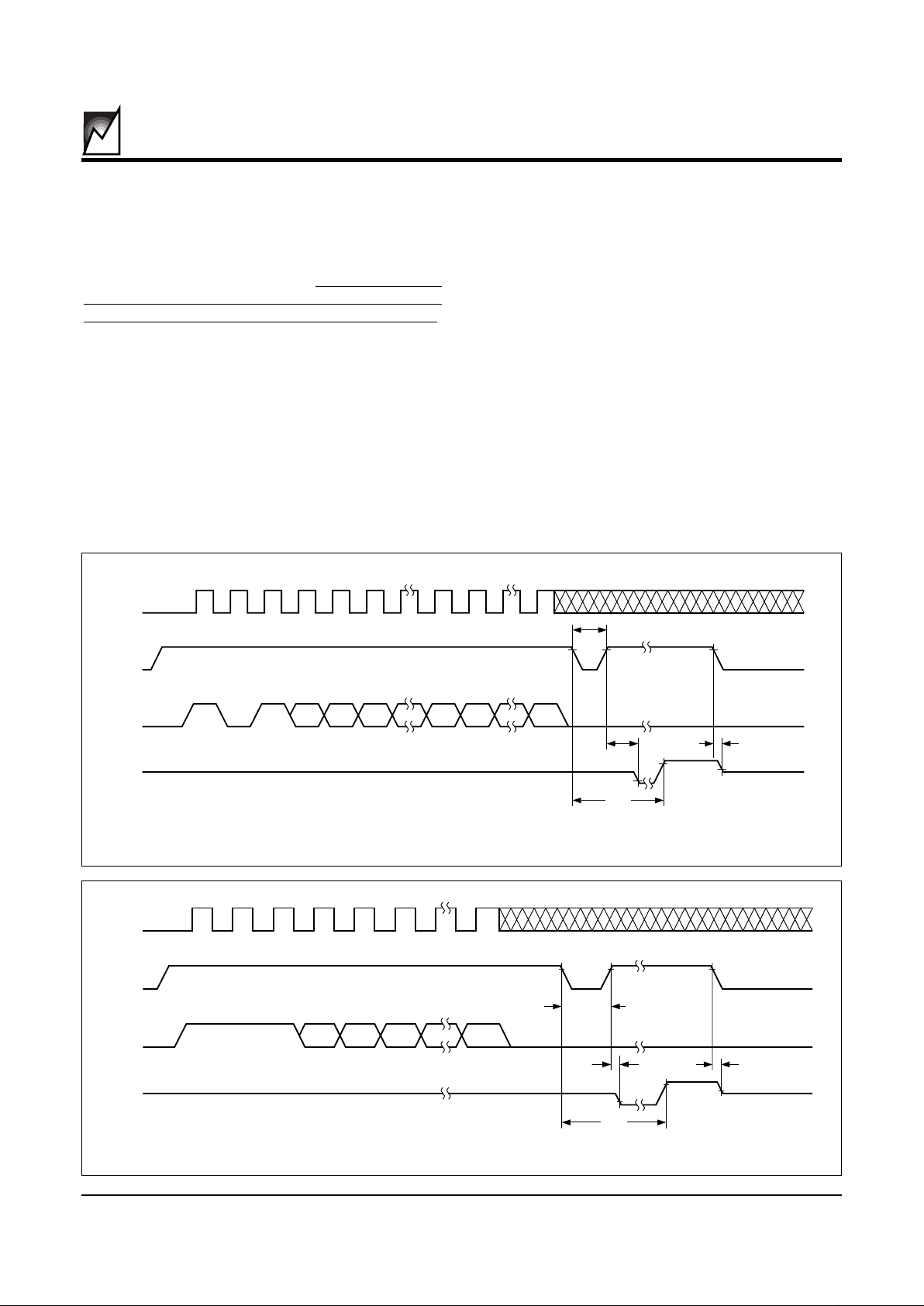
Write
After receiving a WRITE command, address and the
data, the CS (Chip Select) pin must be deselected for a
minimum of 250ns (t
CSMIN
). The falling edge of CS will
start automatic erase and write cycle to the memory
location specified in the instruction. The ready/busy
status of the S93VP662/VP663 can be determined by
selecting the device and polling the DO pin.
Erase
Upon receiving an ERASE command and address, the
CS (Chip Select) pin must be deslected for a minimum
of 250ns (t
CSMIN
). The falling edge of CS will start the
auto erase cycle of the selected memory location. The
ready/busy status of the S93VP662/VP663 can be
determined by selecting the device and polling the DO
pin. Once cleared, the content of a cleared location
returns to a logical “1” state.
Figure 1. Sychronous Data Timing
Figure 2. Read Instruction Timing
SK
2019 ILL 3 1.0
DI
CS
DO
t
DIS
t
PD0,tPD1
t
CSMIN
t
CSS
t
DIS
t
DIH
t
SKHI
t
CSH
VALID VALID
DATA VALID
t
SKLOW
SK
2019 ILL4 1.0
CS
DI
DO
t
CS
STANDBY
t
HZ
HIGH-ZHIGH-Z
11 0
ANA
N–1
A
0
0
DND
N–1
D1D
0
t
PD0
Page 4
4
S93VP662/S93VP663
2019 1.1 5/15/98
Erase/Write Enable and Disable
The S93VP662/VP663 powers up in the write disable
state. Any writing after power-up or after an EWDS
(write disable) instruction must first be preceded by the
EWEN (write enable) instruction. Once the write instruction is enabled, it will remain enabled until power to
the device is removed, or the EWDS instruction is sent.
The EWDS instruction can be used to disable all
S93VP662/VP663 write and clear instructions, and will
prevent any accidental writing or clearing of the device.
Data can be read normally from the device regardless
of the write enable/disable status.
Erase All
Upon receiving an ERAL command, the CS (Chip
Select) pin must be deselected for a minimum of 250ns
(t
CSMIN
). The falling edge of CS will start the self clocking
clear cycle of all memory locations in the device. The
clocking of the SK pin is not necessary after the device
has entered the self clocking mode. The ready/busy
status of the S93VP662/VP663 can be determined by
selecting the device and polling the DO pin. Once
cleared, the contents of all memory bits return to a
logical “1” state.
Write All
Upon receiving a WRAL command and data, the CS
(Chip Select) pin must be deselected for a minimum of
250ns (t
CSMIN
). The falling edge of CS will start the self
clocking data write to all memory locations in the device.
The clocking of the SK pin is not necessary after the
device has entered the self clocking mode. The ready/
busy status of the S93VP662/VP663 can be determined
by selecting the device and polling the DO pin. It is not
necessary for all memory locations to be cleared before
the WRAL command is executed.
Figure 3. Write Instruction Timing
Figure 4. Erase Instruction Timing
SK
2019 ILL 5 1.0
CS
DI
DO
t
CS
STANDBY
HIGH-Z
HIGH-Z
101
A
N
A
N-1
A
0
D
N
D
0
BUSY
READY
STATUS
VERIFY
t
SV
t
HZ
t
EW
SK
2019 ILL6 1.0
CS
DI
DO
STANDBY
HIGH-Z
HIGH-Z
1
A
N
A
N-1
BUSY READY
STATUS VERIFY
t
SV
t
HZ
t
EW
t
CS
11
A
0
Page 5

5
S93VP662/S93VP663
2019 1.1 5/15/98
Figure 5. EWEN/EWDS Instruction Timing
Figure 6. ERAL Instruction Timing
SK
2019 ILL 7 1.0
CS
DI
STANDBY
10
0
*
* ENABLE=1 1
DISABLE=00
SK
2019 ILL 8 1.0
CS
DI
DO
t
CS
HIGH-Z
HIGH-Z
10 1
BUSY READY
STATUS VERIFY
t
SV
t
HZ
t
EW
00
STANDBY
Page 6

6
S93VP662/S93VP663
2019 1.1 5/15/98
Figure 7. WRAL Instruction Timing
SK
2019 ILL 10 1.0
CS
DI
DO
t
CS
HIGH-Z
10 1
BUSY READY
STATUS VERIFY
t
SV
t
HZ
t
EW
00
STANDBY
D
O
D
N
INSTRUCTION SET
Instruction Start Opcode Address Data Comments
Bit S93VP662 S93VP663 S93VP662 S93VP663
READ 1 10 A8–A0 A7–A0 Read Address AN–A0
ERASE 1 11 A8–A0 A7–A0 Clear Address AN–A0
WRITE 1 01 A8–A0 A7–A0 D7–D0 D15–D0 Write Address AN–A0
EWEN 1 00 11xxx xxxx 11xxx xxx Write Enable
EWDS 1 00 00xxx xxxx 00xxx xxx Write Disable
ERAL 1 00 10xxx xxxx 10xxx xxx Clear All Addresses
WRAL 1 00 11xxx xxxx 01xxx xxx D7–D0 D15–D0 Write All Addresses
2019 PGM T5 1.0
Page 7

7
S93VP662/S93VP663
2019 1.1 5/15/98
D.C. OPERATING CHARACTERISTICS
VCC = +2.7V to +6.0V, unless otherwise specified. TA = -40ºC to +85ºC
Limits
Symbol Parameter Min. Typ. Max. Units Test Conditions
I
CC
Power Supply Current 3 mA DI = 0.0V, fSK = 1MHz
(Operating) VCC = 5.0V, CS = 5.0V,
Output Open
I
SB
Power Supply Current 50 µA CS = 0V
(Standby)
I
LI
Input Leakage Current 2 µAVIN = 0V to V
CC
I
LO
Output Leakage Current 10 µAV
OUT
= 0V to VCC,
(Including ORG pin) CS = 0V
V
IL1
Input Low Voltage -0.1 0.8 V 4.5V≤VCC<5.5V
V
IH1
Input High Voltage 2 VCC+1 V
V
IL2
Input Low Voltage 0 VCCX0.2 V 1.8V≤VCC<2.7V
V
IH2
Input High Voltage VCCX0.7 VCC+1 V
V
OL1
Output Low Voltage 0.4 V 4.5V≤VCC<5.5V
V
OH1
Output High Voltage 2.4 V IOL = 2.1mA
IOH = -400µA
V
OL2
Output Low Voltage 0.2 V 1.8V≤VCC<2.7V
V
OH2
Output High Voltage VCC-0.2 V IOL = 1mA
IOH = -100µA
Note:
(1) The minimum DC input voltage is –0.5V. During transitions, inputs may undershoot to –2.0V for periods of less than 20 ns. Maximum DC
voltage on output pins is VCC +0.5V, which may overshoot to VCC +2.0V for periods of less than 20 ns.
(2) Output shorted for no more than one second. No more than one output shorted at a time.
(3) This parameter is tested initially and after a design or process change that affects the parameter.
(4) Latch-up protection is provided for stresses up to 100 mA on address and data pins from –1V to VCC +1V.
2019 PGM T3 1.0
ABSOLUTE MAXIMUM RATINGS*
Temperature Under Bias ................. –55°C to +125°C
Storage Temperature....................... –65°C to +150°C
Voltage on any Pin with
Respect to Ground
(1)
............ –2.0V to +VCC +2.0V
VCC with Respect to Ground ............... –2.0V to +7.0V
Package Power Dissipation
Capability (Ta = 25°C)................................... 1.0W
Lead Soldering Temperature (10 secs)............ 300°C
Output Short Circuit Current
(2)
........................ 100 mA
*COMMENT
Stresses above those listed under “Absolute Maximum
Ratings” may cause permanent damage to the device.
These are stress ratings only, and functional operation of
the device at these or any other conditions outside of those
listed in the operational sections of this specification is not
implied. Exposure to any absolute maximum rating for
extended periods may affect device performance and
reliability.
RELIABILITY CHARACTERISTICS
Symbol Parameter Min. Max. Units Reference Test Method
N
END
(3)
Endurance 1,000,000 Cycles/Byte MIL-STD-883, Test Method 1033
T
DR
(3)
Data Retention 100 Years MIL-STD-883, Test Method 1008
V
ZAP
(3)
ESD Susceptibility 2000 Volts MIL-STD-883, Test Method 3015
I
LTH
(3)(4)
Latch-Up 100 mA JEDEC Standard 17
2019 PGM T2 1.1
Page 8

8
S93VP662/S93VP663
2019 1.1 5/15/98
A.C. CHARACTERISTICS
Limits
VCC=2.7V-4.5V VCC=4.5V-5.5V Test
SYMBOL PARAMETER Min. Max. Min. Max. UNITS Conditions
t
CSS
CS Setup Time 100 50 ns
t
CSH
CS Hold Time 0 0 ns VIL = 0.45V
t
DIS
DI Setup Time 200 100 ns VIH = 2.4V
t
DIH
DI Hold Time 200 100 ns CL = 100pF
t
PD1
Output Delay to 1 0.5 0.25 µsVOL = 0.8V
t
PD0
Output Delay to 0 0.5 0.25 µsVOH = 2.0v
t
HZ
(1)
Output Delay to High-Z 200 100 ns
t
EW
Program/Erase Pulse Width 10 10 ms
t
CSMIN
Minimum CS Low Time 0.5 0.25 µs
t
SKHI
Minimum SK High Time 0.5 0.25 µs
t
SKLOW
Minimum SK Low Time 0.5 0.25 µs
t
SV
Output Delay to Status Valid 0.5 0.25 µsCL = 100pF
SK
MAX
Maximum Clock Frequency DC 500 DC 1000 KHZ
Note:
(1) This parameter is tested initially and after a design or process change that affects the parameter.
CL = 100pF
2019 PGM T6 1.0
Note:
(1) This parameter is tested initially and after a design or process change that affects the parameter.
PIN CAPACITANCE
Symbol Test Max. Units Conditions
C
OUT
(1)
OUTPUT CAPACITANCE (DO) 5 pF V
OUT
=OV
C
IN
(1)
INPUT CAPACITANCE (CS, SK, DI, ORG) 5 pF VIN=OV
2019 PGM T4 1.0
Page 9

9
S93VP662/S93VP663
2019 1.1 5/15/98
Figure 8. V
LOCK
Timing Diagram
t
PUW
t
GLITCH
t
LDLY
V
LOCK
V
CC
t
PUW
t
LDLY
V
LOCKOUT
V
LOCKOUT
V
LOCKOUT
Internal Action
2019 ILL9 1.0
S24VP662/VP663-2.7 S24VP662/VP663–A S24VP662/VP663–B
Symbol Parameter Min Max Min Max Min Max Unit
V
LOCK
Write Lockout Voltage Level 2.55 2.70 4.25 4.50 4.50 4.75 V
t
PUW
Power-Up Write Delay 130 20 130 270 130 270 ms
t
LDLY
Delay to V
LOCKOUT
555µs
t
GLITCH
Glitch Filter 30 30 30 ns
V
LOCK
CIRCUIT AC and DC ELECTRICAL CHARACTERISTICS
TA = -40°C to +85°C
2019 PGM T1 1.3
Page 10

10
S93VP662/S93VP663
2019 1.1 5/15/98
.228 (5.80)
.244 (6.20)
.016 (.40)
.035 (.90)
.020 (.50)
.010 (.25)
x45°
.0192 (.49)
.0138 (.35)
.061 (1.75)
.053 (1.35)
.0098 (.25)
.004 (.127)
.05 (1.27) TYP.
.275 (6.99) TYP.
.030 (.762) TYP.
8 Places
.050 (1.27) TYP.
.050 (1.270) TYP.
8 Places
.157 (4.00)
.150 (3.80)
.196 (5.00)
1
.189 (4.80)
FOOTPRINT
8pn JEDEC SOIC ILL.2
.375
(9.525)
PIN 1 INDICATOR
.015 (.381) Min.
.130 (3.302)
.100 (2.54)
TYP.
.018 (.457)
TYP.
.060 ± .005
(1.524) ± .127
TYP.
.130 (3.302)
SEATING PLANE
.070 (1.778)
.0375 (0.952)
.300 (7.620)
5°-7°TYP.
(4 PLCS)
.350 (8.89)
.009 ± .002
(.229 ± .051)
0°-15°
.250
(6.350)
8pn PDIP/P ILL.3
8 Pin SOIC (Type S) Package JEDEC (150 mil body width)
8 Pin PDIP (Type P) Package
Page 11

11
S93VP662/S93VP663
2019 1.1 5/15/98
ORDERING INFORMATION
Operating Temperature Range
Blank = 0°C to +70°C
I = -40°C to +85°C
Package
P = 8 Lead PDIP
S = 8 Lead SOIC
Tape and Reel Option
TE7 = 7 inch Reel, 500 units/reel
TE13 = 13 inch Reel, 2000 units/reel
Operating V oltage Range
A = 4.5V to 5.5V V
LOCK
Min @4.25V
B = 4.5V to 5.5V V
LOCK
Min @4.50V
2.7 = 2.7V to 5.5V V
LOCK
Min @2.55V
S93VPxx P I -2.7 TE7
Base Part Number
S93VP662 = 8-bit data configuration
S93VP663 = 16-bit data configuration
2019 ILL11 1.1
Page 12

12
S93VP662/S93VP663
2019 1.1 5/15/98
NOTICE
SUMMIT Microelectronics, Inc. reserves the right to make changes to the products contained in this publication in order to improve
design, performance or reliability. SUMMIT Microelectronics, Inc. assumes no responsibility for the use of any circuits described
herein, conveys no license under any patent or other right, and makes no representation that the circuits are free of patent
infringement. Charts and schedules contained herein reflect representative operating parameters, and may vary depending upon
a user’s specific application. While the information in this publication has been carefully checked, SUMMIT Microelectronics, Inc.
shall not be liable for any damages arising as a result of any error or omission.
SUMMIT Microelectronics, Inc. does not recommend the use of any of its products in life support applications where the failure or
malfunction of the product can reasonably be expected to cause failure of the life support system or to significantly affect its safety
or effectiveness. Products are not authorized for use in such applications unless SUMMIT Microelectronics, Inc. receives written
assurances, to its satisfaction, that: (a) the risk of injury or damage has been minimized; (b) the user assumes all such risks; and
(c) potential liability of SUMMIT Microelectronics, Inc. is adequately protected under the circumstances.
© Copyright 1998 SUMMIT Microelectronics, Inc.
 Loading...