

Page 1

Intel Corporation assumes no responsibility for the use of any circuitry other than circuitry embodied in an Intel product. No other circuit patent
licenses are implied. Information contained herein supersedes previously published specifications on these devices from Intel.
© INTEL CORPORATION, 1995 September 1995 Order Number: 272543-001
®
8XC196MH INDUSTRIAL MOTOR CONTROL
CHMOS MICROCONTROLLER
The 8XC196MH is a member of Intel’s family of 16-bit MCS® 96 microcontrollers. It is designed primarily to
control three-phase AC induction and DC brushless motors. It features an enhanced three-phase waveform
generator specifically designed for use in “inverter” motor-control applications. This peripheral provides pulsewidth modulation and three-phase sine wave generation with minimal CPU intervention. It generates three
complementary non-overlapping PWM pulses with resolutions of 0.125 µs (edge triggered) or 0.250 µs
(centered).
The 8XC196MH has two dedicated serial port peripherals, allowing less software overhead. The watchdog timer
can be programmed with one of four time options.
The 8XC196MH is available without internal memory (80C196MH), with 32 Kbytes of factory programmed
OTPROM* (83C196MH), or with 32 Kbytes of user programmable OTPROM* (87C196MH). It is available in
three packages: 84-lead PLCC, 80-lead Shrink EIAJ/QF P, and 64-lead SDIP. The 64-lead package does not
contain pins for the P5.1/INST and P6.7/PWM1 signals.
Operational characteristics are guaranteed over the temperat ure range of
– 40°C to + 85°C.
*One-Time Programmable Read-Only Memory (OTPROM) is similar to EPROM but comes in an unwindowed package and
cannot be erased. It is user programmable.
n
High Performance CHMOS 16-bit CPU
n
16 MHz Operating Frequency
n
32 Kbytes of On-chip OTPROM/RO M
n
744 Bytes of On-chip Register RAM
n
Register-to-register Archi tectu re
n
16 Prioritized Interrupt Sources
n
Peripheral Transaction Server (PTS) with 15
Prioritized Sources
n
Up to 52 I/O Lines
n
3-phase Complementary Waveform Generator
n
8-channel 8- or 10-bit A/D with Samp l e and
Hold
n
2-channel UART
n
Event Processor Array (EPA) with 2 Highspeed Capture/Com pare Mo d ules an d 4 Highspeed Compare-only Modules
n
Two Programmable 16-bit Timers with
Quadrature Countin g Input s
n
Two Pulse-width Modulator (PWM) Outputs
with High Drive Capability
n
Flexible 8- or 16-bit External Bus
n
1.75 µs 16 × 16 Multipl y
n
3 µs 32/16 Divide
n
Extended Temperature Avai lab le
n
Idle and Powerdo w n Mod es
n
Watchdog Timer
Page 2
8XC196MH INDUSTRIAL MOTO R CONTRO L CHMO S MICRO CO NTR OLL ER
®
2
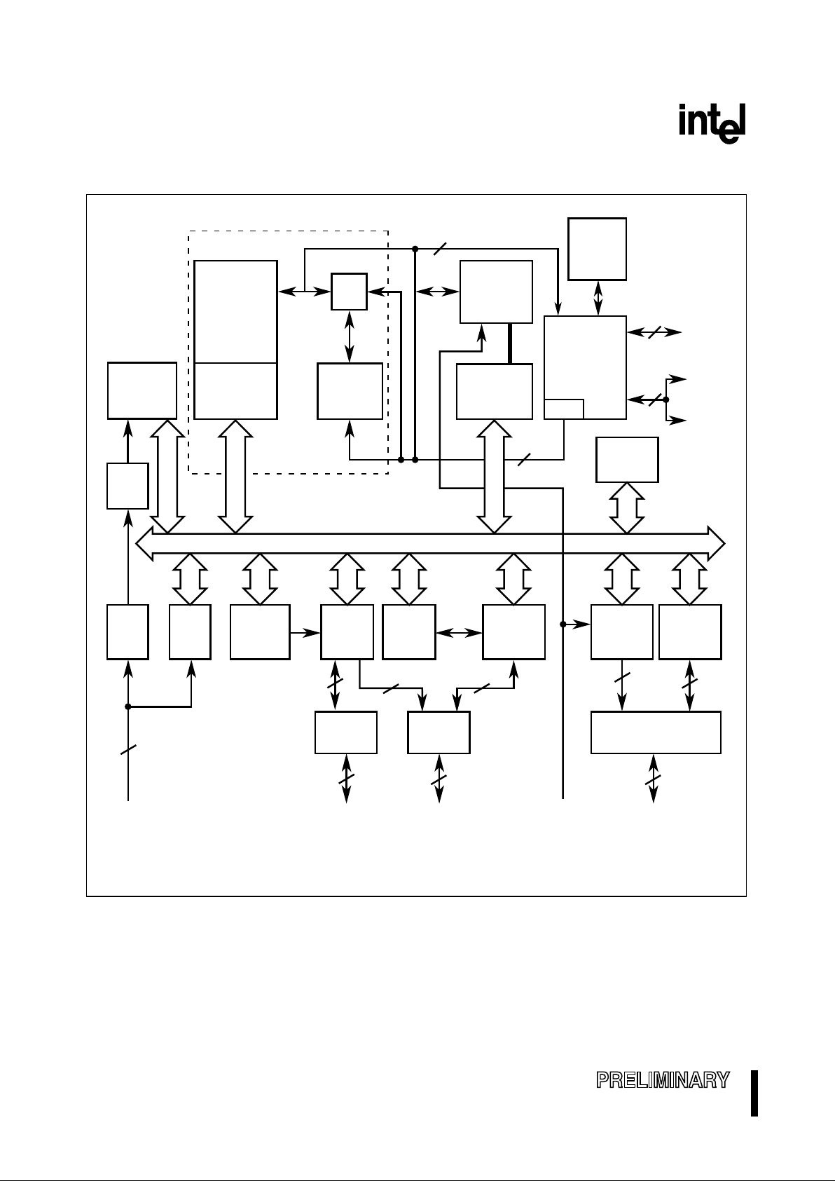
Figure 1. 8XC196MH Block Diagram
Timer 1
Timer 2
Event
Processor
Array
3-Phase
Waveform
Generator
Port 2
Microcode
Engine
RALU
CPU
Peripheral
Transaction
Server
32K
On-chip
ROM/
OTPROM
Port 4
AD15:8
Port 3
AD7:0
Port 5
Control
Signals
Interrupt
Controller
16
8
744
Byte
Register
File
Memory
Controller
Queue
Port 6
Port 6
Waveform
Generator
A2542-01
Port 2
SIO, EPA
2 Capture/Compare
4 Compare
Port 1
SIO 0
SIO 1
Port 1
Serial I/O
Baud
Rate
Generator
Port 0
A/D
Port 0
8/10-Bit
A/D
Converter
Mux
S/H
24 Bytes
CPU SFRs
Watchdog
Timer
EXTINT
PWM0
PWM1
88
4
4
26
8
6
2
8
8
Page 3

8XC196MH INDUSTRIAL MOTOR CONT ROL CHM OS MICRO CO NTR OLL ER
®
3
PROCESS INFORMATION
This device is manufactured on PX29.5, a CHMOS IV
process. Additional process and reliability information
is available in Intel’s
Components Quality and
Reliability
Handbook (order number 210997).
All thermal impedance data is approximate for static
air conditions at 1 watt of power dissipation. Values
will change depending on operating conditions and
the application. The Intel
Packaging
Handbook (order
number 240800) describes I ntel’s thermal impedance
test methodology.
Table 1. Thermal Characteristics
Package Type θ
JA
θ
JC
84-lead PLCC 33°C/W 11°C/W
80-lead QFP 56°C/W 12°C/W
64-lead SDIP 56°C/W N/A
Figure 2. The 8XC196MH Family Nomenclat ure
X XX 8 X C 196 XX XX
Device Speed:
Product Family:
No Mark = 16 MHz
K
x
, Mx, N
x
CHMOS Technology
Program Memory Options:
0 = ROMless, 3 = ROM, 7 = OTPROM
Package - Type Options:
Temperature and Burn In Options:
A2759-01
D = SDIP, N = PLCC, S = QFP
No Mark = –40˚C – +85˚C Ambient
with Intel Standard Burn-In
Page 4
8XC196MH INDUSTRIAL MOTO R CONTRO L CHMO S MICRO CO NTR OLL ER
®
4
Table 2. 8XC196MH Memory Map
Address
(1)
Description Notes
0FFFFH
0A000H
External Memory
09FFFH
02080H
Internal ROM/OTPROM or External Mem ory
0207FH
0205EH
Reserved 1, 2
0205DH
02040H
PTS Vectors
0203FH
02030H
Interrupt Vectors (upper)
0202FH
02020H
ROM/OTPROM Security Key
0201FH
0201CH
Reserved 1, 2
0201BH Reserved (must contain 20H)
0201AH CCB1
02019H Reserved (must contain 20H)
02018H CCB0
02017H
02014H
Reserved
02013H
02000H
Interrupt Vectors (lower)
01FFFH
01F00H
Internal SFRs 1
1EFFH
300H
External Memory
2FFH
18H
Register RAM 3
17H
00H
CPU SFRs 1
NOTES:
1. Unless otherwise noted, write 0FFH to reserved mem ory locations and write 0 to reserved SFR bits.
2. WARNING: The contents and/or func tion of reserved locations may change with future revisions of the
device.
3. Code executed in locations 0000H to 02FFH will be forced external.
Page 5
8XC196MH INDUSTRIAL MOTOR CONT ROL CHM OS MICRO CO NTR OLL ER
®
5
Table 3. Signals Arranged by Fun cti onal Categ ori e s
Address & Data Programming Control Input/Output Input/Output (Cont’d)
AD15:0 AINC# P0.0/ACH0 P2.5/COMP1
CPVER P0.1/ACH1 P2.6/COMP2
Bus Control & Status PACT# P0.2/ACH2 P2.7/SCLK1#/BCLK1
ALE/ADV# PALE# P0.3/ACH3 P3.7:0
BHE#/WRH# PBUS15:0 P0.4/ACH4 P4.7:0
BUSWIDTH PMODE.3:0 P0.5/ACH5 P5.7:0
INST PROG# P0.6/ACH6/T1CLK P6.0/WG1#
READY PVER P0.7/ACH7/T1DIR P6.1/WG1
RD# P1.0/TXD0 P6.2/WG2#
WR#/WRL# Processor Control P1.1/RXD0 P6.3/WG2
EA# P1.2/TXD1 P6.4/WG3#
Power & Ground EXTINT P1.3/RXD1 P6.5/WG3
ANGND NMI P2.0/EPA0 P6.6/PWM0
V
CC
ONCE# P2.1/SCLK0#/BCLK0 P6.7/PWM1
V
PP
RESET# P2.2/EPA1
V
REF
XTAL1 P2.3/COMP3
V
SS
XTAL2 P2.4/COMP0
NOTE: The following signals are not available in the 64-pin package: P5.1, P6.7, INST, and PWM1.
Page 6
8XC196MH INDUSTRIAL MOTO R CONTRO L CHMO S MICRO CO NTR OLL ER
®
6
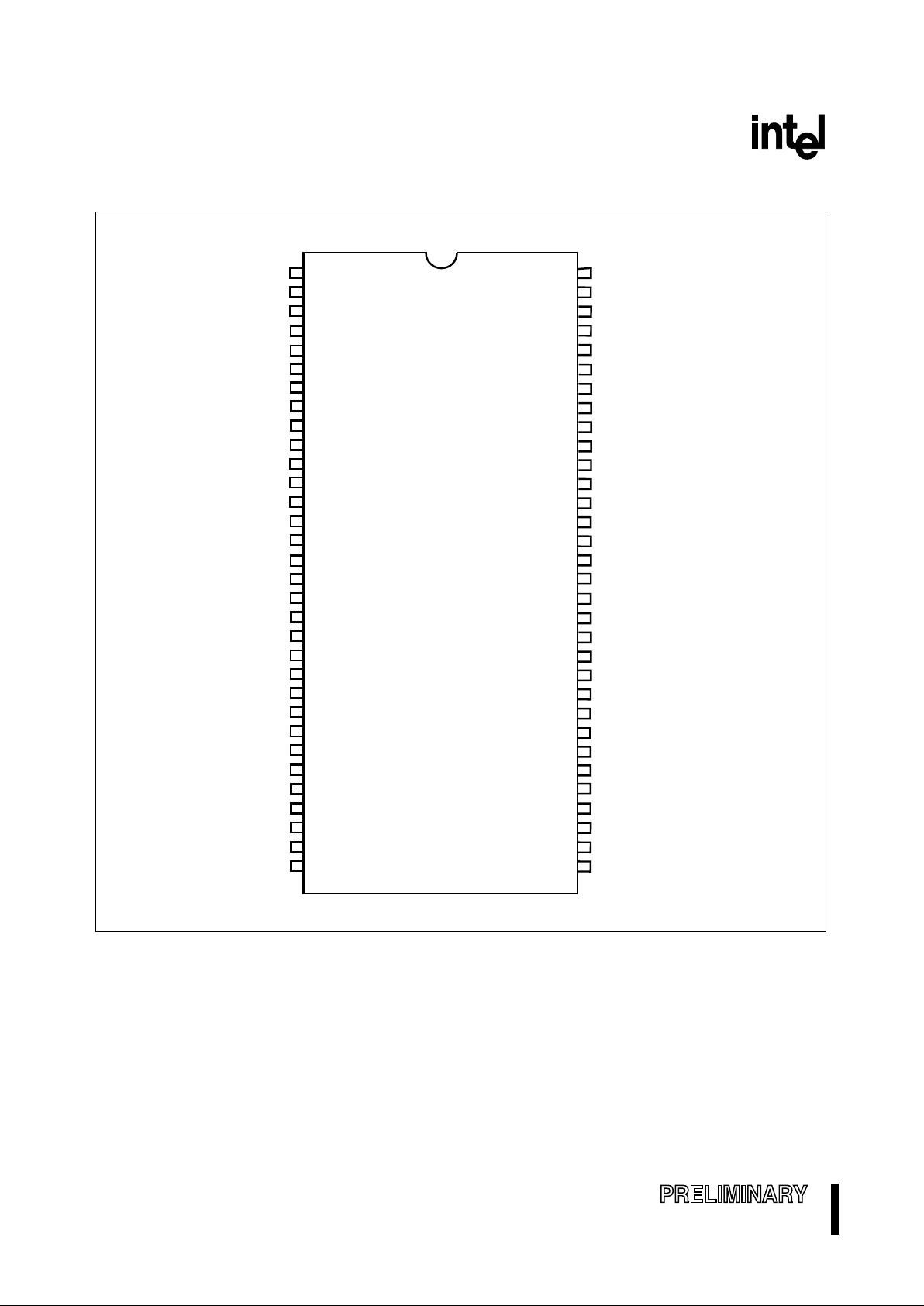
Figure 3. 8XC196MH 64-lead Shrink DIP (SDIP) Package
1
2
3
4
5
6
7
8
9
10
11
12
13
14
15
16
17
18
19
20
21
22
23
24
25
26
27
28
29
30
31
32
64
63
62
61
60
59
58
57
56
55
54
53
52
51
50
49
48
47
46
45
44
43
42
41
40
39
38
37
36
35
34
33
U8XC196MH
TOP VIEW
(Looking down
on component side of
PC board)
P5.6/READY
P5.4/ONCE#
EXTINT
V
SS
XTAL1
XTAL2
P6.6/PWM0
P2.7/SCLK1#/BCLK1
P2.6/COMP2/CPVER
P2.5/COMP1/PACT#
P2.4/COMP0/AINC#
P2.3/COMP3
P2.2/EPA1/PROG#
P2.1/SCLK0#/BCLK0/PALE#
P2.0/EPA0/PVER
P0.0/ACH0
P0.1/ACH1
P0.2/ACH2
P0.3/ACH3
P0.4/ACH4/PMODE.0
P0.5/ACH5/PMODE.1
V
REF
ANGND
P0.6/ACH6/T1CLK/PMODE.2
P0.7/ACH7/T1DIR/PMODE.3
P1.0/TXD0
P1.1/RXD0
P1.2/TXD1
P1.3/RXD1
P6.0/WG1#
P6.1/WG1
P6.2/WG2#
V
SS
P5.0/ALE/ADV#
V
PP
P5.3/RD#
P5.5/BHE#/WRH#
P5.2/WR#/WRL#
P5.7/BUSWIDTH
P4.6/AD14/PBUS.14
P4.5/AD13/PBUS.13
P4.7/AD15/PBUS.15
V
CC
P4.4/AD12/PBUS.12
P4.3/AD11/PBUS.11
P4.2/AD10/PBUS.10
P4.1/AD9/PBUS.9
P4.0/AD8/PBUS.8
P3.7/AD7/PBUS.7
P3.6/AD6/PBUS.6
P3.5/AD5/PBUS.5
P3.4/AD4/PBUS.4
P3.3/AD3/PBUS.3
P3.2/AD2/PBUS.2
P3.1/AD1/PBUS.1
P3.0/AD0/PBUS.0
RESET#
NMI
EA#
V
SS
V
CC
P6.5/WG3
P6.4/WG3#
P6.3/WG2
A2572-01
Page 7
8XC196MH INDUSTRIAL MOTOR CONT ROL CHM OS MICRO CO NTR OLL ER
®
7
Table 4. 64-lead Shrink DIP (SDI P) Pi n Assi gnme nt
Pin Name Pin Name Pin Name Pin Name
1V
SS
17 P3.7/AD7
/PBUS.7
33 P6.2/WG2# 49 P0.0/A C H0
2 P5.0/A LE/ADV# 18 P3.6/AD6
/PBUS.6
34 P6.1/WG1 50 P2.0/EPA0/PVER
3V
PP
19 P3.5/AD5
/PBUS.5
35 P6.0/WG1# 51 P2.1/SCLK0#
/BCLK0/PALE#
4 P5.3/RD# 20 P3.4/AD4
/PBUS.4
36 P1.3/RXD1 52 P2.2/EPA1
/PROG#
5 P5.5/B HE#/WRH# 21 P3.3/AD3
/PBUS.3
37 P1.2/TXD1 53 P2. 3/CO M P3
6 P5.2/W R#/WRL# 22 P3.2/AD2
/PBUS.2
38 P1.1/RXD0 54 P2.4/COMP0
/AINC#
7 P5.7/B USW I DTH 23 P3.1/AD1
/PBUS.1
39 P1.0/TXD0 55 P2. 5/CO M P1
/PACT#
8 P4.6/A D 14
/PBUS.14
24 P3.0/AD0
/PBUS.0
40 P0.7/ACH7/T1DIR
/PMODE.3
56 P2.6/COMP2
/CPVER
9 P4.5/A D 13
/PBUS.13
25 RESET# 41 P0.6/ACH6
/T1CLK/PMODE .2
57 P2.7/SCLK1#
/BCLK1
10 P4.7/AD15
/PBUS.15
26 NMI 42 ANGND 58 P6.6/PWM0
11 V
CC
27 EA# 43 V
REF
59 XTAL2
12 P4.4/AD12
/PBUS.12
28 V
SS
44 P0.5/ACH5
/PMODE.1
60 XTAL1
13 P4.3/AD11
/PBUS.11
29 V
CC
45 P0.4/ACH4
/PMODE.0
61 V
SS
14 P4.2/AD10
/PBUS.10
30 P6.5/WG3 46 P0.3/ACH3 62 EXTINT
15 P4.1/AD9/PBUS.9 31 P6.4/WG3# 47 P0.2/ACH2 63 P5.4/ONCE#
16 P4.0/AD8/PBUS.8 32 P6.3/WG2 48 P0.1/ACH1 64 P5.6/READY
Page 8
8XC196MH INDUSTRIAL MOTO R CONTRO L CHMO S MICRO CO NTR OLL ER
®
8
Figure 4. 8XC196MH 84-lead PLCC Package
12
13
14
15
16
17
18
19
20
21
22
23
24
25
26
27
28
29
30
31
32
74
73
72
71
70
69
68
67
66
65
64
63
62
61
60
59
58
57
56
55
54
33
34
35
36
37
38
39
40
41
42
43
44
45
46
47
48
49
50
51
52
53
11
10
987654321
84
83
82
81
80
79
78
77
76
75
P2.5/COMP1/PACT#
P2.4/COMP0/AINC#
NC
NC
P2.7/SCLK1#/BCLK1
P2.3/COMP3
P2.2/EPA1/PROG#
NC
NC
P2.1/SCLK0#/BCLK0/PALE#
P2.0/EPA0/PVER
NC
P0.0/ACH0
P0.1/ACH1
P0.2/ACH2
P0.3/ACH3
P0.4/ACH4/PMODE.0
P0.5/ACH5/PMODE.1
V
REF
ANGND
P0.6/ACH6/T1CLK/PMODE.2
P4.7/AD15/PBUS.15
P4.6/AD14/PBUS.14
VCC
P4.5/AD13/PBUS.13
NC
P4.4/AD12/PBUS.12
P4.3/AD11/PBUS.11
P4.2/AD10/PBUS.10
P4.1/AD9/PBUS.9
P4.0/AD8/PBUS.8
NC
NC
P3.7/AD7/PBUS.7
P3.6/AD6/PBUS.6
P3.5.AD5/PBUS.5
P3.4/AD4/PBUS.4
P3.3/AD3/PBUS.3
P3.2/AD2/PBUS.2
P3.1/AD1/PBUS.1
P3.0/AD0/PBUS.0
NC
P5.7/BUSWIDTH
P5.2/WR#/WRL#
NC
P5.5/BHE#/WRH#
P5.3/RD#
V
PP
P5.0/ALE/ADV#
V
SS
P5.1/INST
P5.6/READY
P5.4/ONCE#
EXTINT
V
SS
XTAL1
XTAL2
NC
NC
NC
P6.6/PWM0
P6.7/PWM1
P2.6/COMP2/CPVER
RESET#
NMI
NC
EA#
V
SS
NCVCC
P6.5/WG3
P6.4/WG3#
P6.3/WG2
V
SS
P6.2/WG2#
P6.1/WG1
P6.0/WG1#
P1.3/RXD1
P1.2/TXD1
NC
NC
P1.1/RXD0
P1.0/TXD0
P0.7/ACH7/T1DIR/PMODE.3
N8XC196MH
TOP VIEW
(Looking down
on component side of
PC board)
A2573-02
Page 9
8XC196MH INDUSTRIAL MOTOR CONT ROL CHM OS MICRO CO NTR OLL ER
®
9
Table 5. 84-lead PLCC Pin Assig nme nt
Pin Name Pin Name Pin Name Pin Name
1 P5.4/ONCE# 22NC 43V
SS
64 P2.0/EPA0/PVER
2 P5.6/RE ADY 23 NC 44 P6.2/WG2# 65 P2.1/SCLK0#
/BCLK0/PALE#
3 P5.1/INST 24 P3.7/AD7
/PBUS.7
45 P6.1/WG1 66 NC
4V
SS
25 P3.6/AD6
/PBUS.6
46 P6.0/WG1# 67 NC
5 P5.0/ALE/ADV# 26 P3.5/AD5
/PBUS.5
47 P1.3/RXD1 68 P2.2/EPA1
/PROG#
6V
PP
27 P3.4/AD4
/PBUS.4
48 P1.2/TXD1 69 P2. 3/CO M P3
7 P5.3/RD# 28 P3.3/AD3
/PBUS.3
49 NC 70 P2.7/SCLK1#
/BCLK1
8 P5.5/BHE#/WRH# 29 P3.2/AD2
/PBUS.2
50 NC 71 NC
9 NC 30 P3.1/AD1
/PBUS.1
51 P1.1/RXD0 72 NC
10 P5.2/WR#/WRL # 31 P3.0/AD0
/PBUS.0
52 P1.0/TXD0 73 P2. 4/CO M P0
/AINC#
11 P5.7/BUSWIDTH 32 NC 53 P0.7/ACH7
/T1DIR/PMODE. 3
74 P2.5/COMP1
/PACT#
12 P4.7/AD15
/PBUS.15
33 RESET# 54 P0.6/ACH6
/T1CLK/PMOD E.2
75 P2.6/COMP2
/CPVER
13 P4.6/AD14
/PBUS.14
34 NMI 55 ANGND 76 P6.7/PWM1
14 V
CC
35 NC 56 V
REF
77 P6.6/PWM0
15 P4.5/AD13
/PBUS.13
36 EA# 57 P0.5/ACH5
/PMODE.1
78 NC
16 NC 37 V
SS
58 P0.4/ACH4
/PMODE.0
79 NC
17 P4.4/AD12
/PBUS.12
38 NC 59 P0.3/ACH3 80 NC
18 P4.3/AD11
/PBUS.11
39 V
CC
60 P0.2/ACH2 81 XTAL2
19 P4.2/AD10
/PBUS.10
40 P6.5/WG3 61 P 0.1/ ACH1 82 XTAL1
20 P4.1/AD9/PBUS.9 41 P6.4/WG3 # 62 P0.0/ ACH0 83 V
SS
21 P4.0/AD8/PBUS.8 42 P6.3/WG 2 63 NC 84 EXTINT
Page 10
8XC196MH INDUSTRIAL MOTO R CONTRO L CHMO S MICRO CO NTR OLL ER
®
10
Figure 5. 8XC196MH 80-lead Shrink EIAJ/Q FP Packag e
1
2
3
4
5
6
7
8
9
10
12
17
13
14
16
18
19
11
15
20
21
24
25 26 28 2927
23
22
3938
37343230 31 33 35
36
40
42
41
43
44
45
46
47
48
49
52
53
50
51
55
54
56
57
59
58
60
61
62
63
64
65
6667
68
6973747679 77
75
72 71 70
80
78
P6.7/PWM1
P2.6/COMP2/CPVER
P2.5/COMP1/PACT#
P2.4/COMP0/AINC#
NC
NC
P2.7/SCLK1#/BCLK1
P2.3/COMP3
P2.2/EPA1/PROG#
P2.0/EPA0/PVER
NC
NC
P0.6/ACH6/T1CLK/PMODE.2
NC
P2.1/SCLK0#/BCLK0/PALE#
ANGND
P0.0/ACH0
P0.1/ACH1
P0.2/ACH2
P0.3/ACH3
P0.4/ACH4/PMODE.0
V
REF
P0.5/ACH5/PMODE.1
P0.7/ACH7/T1DIR/PMODE.3
P4.7/AD15/PBUS.15
P5.2/WR#/WRL#
P5.7/BUSWIDTH
P4.6/AD14/PBUS.14
V
CC
P4.5/AD13/PBUS.13
NC
P4.3/AD11/PBUS.11
P4.4/AD12/PBUS.12
P4.2/AD10/PBUS.10
P3.7/AD7/PBUS.7
P4.1/AD9/PBUS.9
P4.0/AD8/PBUS.8
P3.6/AD6/PBUS.6
P3.4/AD4/PBUS.4
P3.3/AD3/PBUS.3
P3.1/AD1/PBUS.1
P3.0/AD0/PBUS.0
NMI
NC
EA#
RESET#
P3.5/AD5/PBUS.5
P3.2/AD2/PBUS.2
V
SS
NC
P6.4/WG3#
P6.1/WG1
V
CC
P6.5/WG3
P6.3/WG2
V
SS
P6.2/WG2#
P1.3/RXD1
P6.0/WG1#
P1.2/TXD1
NC
NC
P1.1/RXD0
P1.0/TXD0
V
PP
P5.3/RD#
P5.1/INST
P5.0/ALE/ADV#
P5.4/ONCE#
P5.6/READY
VSSXTAL1
EXTINT
XTAL2NCNC
P6.6/PWM0
NC
P5.5/BHE#/WRH#
V
SS
S8XC196MH
TOP VIEW
(Looking down
on component side of
PC board)
A2574-01
Page 11
8XC196MH INDUSTRIAL MOTOR CONT ROL CHM OS MICRO CO NTR OLL ER
®
11
Table 6. 80-lead Shrink EIAJ/QFP Pin Assignment
Pin Name Pin Name Pin Name Pin Name
1 P5.2/WR#/WRL# 21 NC 41 P0.7/ACH7/T1DIR
/PMODE.3
61 P2.4/COMP0
/AINC#
2 P5.7/BUSWIDTH 22 RESET# 42 P0.6/ACH6
/T1CLK/PMODE.2
62 P2.5/COMP1
/PACT#
3 P4.7/AD15
/PBUS.15
23 NMI 43 ANGND 63 P2.6/COMP2
/CPVER
4 P4.6/AD14
/PBUS.14
24 EA# 44 V
REF
64 P6.7/PWM1
5V
CC
25 V
SS
45 P0.5/ACH5
/PMODE.1
65 P6.6/PWM0
6 P4.5/AD13
/PBUS.13
26 NC 46 P0.4/ACH4
/PMODE.0
66 NC
7NC 27V
CC
47 P0.3/ACH3 67 NC
8 P4.4/AD12
/PBUS.12
28 P6.5/WG3 48 P0.2/ACH2 68 NC
9 P4.3/AD11
/PBUS.11
29 P6.4/WG3# 49 P0.1/ACH1 69 XTAL2
10 P4.2/AD10
/PBUS.10
30 P6.3/WG2 50 P0.0/ACH0 70 XTAL1
11 P4.1/AD9/PBUS.9 31 V
SS
51 NC 71 V
SS
12 P4.0/AD8/PBUS.8 32 P6.2/WG2# 52 P2.0/EPA0/PVER 72 EXTINT
13 P3.7/AD7/PBUS.7 33 P6.1/WG1 53 P2.1/SCLK0#
/BCLK0/PALE#
73 P5.4/ONCE#
14 P3.6/AD6/PBUS.6 34 P6.0/WG1# 54 NC 74 P5.6/READY
15 P3.5/AD5/PBUS.5 35 P1.3/RXD1 55 NC 75 P5.1/INST
16 P3.4/AD4/PBUS.4 36 P1.2/TXD1 56 P2.2/EPA1
/PROG#
76 V
SS
17 P3.3/AD3/PBUS.3 37 NC 57 P2.3/COMP3 77 P5.0/ALE/ADV#
18 P3.2/AD2/PBUS.2 38 NC 58 P2.7/SCLK1#
/BCLK1
78 V
PP
19 P3.1/AD1/PBUS.1 39 P1.1/RXD0 59 NC 79 P5.3/RD#
20 P3.0/AD0/PBUS.0 40 P1.0/TXD0 60 NC 80 P5.5/BHE#/WRH#
Page 12

8XC196MH INDUSTRIAL MOTO R CONTRO L CHMO S MICRO CO NTR OLL ER
®
12
PIN DESCRIPTIONS
Table 7. Signal Descriptions
Signal
Name
Type Description
Multiplexed
With
ACH7
ACH6
ACH5
ACH4
ACH3:0
I Analog Channels. These pins are analog inputs to the A/D
converter.
These pins are multiplexed with the port 0 pins. While it is
possible for the pins to function simultaneously as analog and
digital inputs, this is not recommended because reading the
port while a conversion is in process can produce unreliable
conversion results.
The ANGND and V
REF
pins must be connected for the A/D
converter and the multiplexed port pins to function.
P0.7/T1DIR/PMO DE .3
P0.6/T1CLK/PMODE.2
P0.5/PMODE.1
P0.4/PMODE.0
P0.3:0
AD15:8
AD7:0
I/O Address/Data Lines. The se pins provide a multiplexed
address and data bus. During the address phase of the bus
cycle, address bits 0–15 are presented on the bus and can
be latched using ALE or ADV#. During the data phase, 8- or
16-bit data is transferred.
P4.7:0/PBUS.15:8
P3.7:0/PBUS.7:0
ADV# O Address Valid. This active-low output signal is asserted only
during external memory accesses.
ADV# indicates that valid address information is available on
the system address/data bus. The signal remains low while a
valid bus cycle is in progress and is returned high as soon as
the bus cycle completes.
An external latch can use the ADV# signal to demultiplex the
address from the address/data bus. Used with a decoder,
ADV# can generate chip-selects for external memory.
P5.0/ALE
AINC# I Auto Increment. In slave programming mode, this active-low
input signal enables the autoincrement mode. Auto increment
allows reading from or writing to sequential OTPROM
locations without requiring address transactions across the
programming bus for each read or write.
P2.4/COMP0
ALE O Address Latch En ab le. This act ive-high output signa l is
asserted only during external memory cycles.
ALE signals the start of an external bus cycle and indicates
that valid address information is available on the system
address/data bus. ALE differs from ADV# in that it is not
returned high until a new bus cycle is to begin.
An external latch can use ALE to demultiplex the address
from the address/data bus.
P5.0/ADV#
ANGND GND Analog Ground. Reference ground for the A/D convert er
and the logic used to read port 0. ANGND must be held at
nominally the same potential as V
SS
.
—
BCLK1
BCLK0
I Serial Communications Baud Clock 0 and 1. BCLK0 and 1
are alternate clock sources for the serial ports. The maximum
input frequency is F
OSC
/4.
P2.7/SCLK1#
P2.1/SCLK0#/PALE#
Page 13

8XC196MH INDUSTRIAL MOTOR CONT ROL CHM OS MICRO CO NTR OLL ER
®
13
BHE# O Byte High Enable. During 16-bit bus cycles, this active-low
output signal is asserted for word reads and writes and for
high-byte reads and writes to external memory. BHE#
indicates that valid data is being transferred over the upper
half of the system address/data bus.
BHE#, in conjunction with A0, selects the memory byte to be
accessed:
BHE# A0 Byte(s) Accessed
0 0 both bytes
0 1 high byte only
1 0 low byte only
P5.5/WRH#
BUSWIDTH I Bus Width. When enabled in the chip configuration register,
this active-high input signal dynamically selects the bus width
of the bus cycle in progress. When BUSWIDTH is high, a 16bit bus cycle occurs; when BUSWIDTH is low, an 8-bit bus
cycle occurs. BUSWIDTH is active during a CCR fetc h.
P5.7
COMP3
COMP2
COMP1
COMP0
O Event Processor Array (EPA) Compare Pins. These
signals are the output of the EPA compare modules. These
pins are multiplexed with other signals and may be
configured as standard I/O.
P2.3
P2.6/CPVER
P2.5/PACT#
P2.4/AINC#
CPVER O Cumulative Program Verification. This active-high output
signal indicates whether any verify errors have occurred
since the device entered programming mode. CPVER
remains high until a verify error occurs, at which time it is
driven low. Once an error occurs, CPVER remains low until
the device exits programming mode. When high, CPVER
indicates that all locations have programmed correctly since
the device entered programming mode.
P2.6/COMP2
EA# I External Access. This active-low input signal directs
memory accesses to on-chip or off-chip memory. If EA# is
low, the memory access is off-chip. If EA# is high and the
memory address is within 2000H–2FFFH, the access is to
on-chip ROM or OTPROM. Otherwise, an access with EA#
high is to off-chip memory.
EA# is sampled only on the rising edge of RESET#.
If EA# = V
EA
on the rising edge of RESET#, the device enters
the programming mode selected by PMODE.3:0.
For devices without ROM, EA# must be tied low.
—
EPA1
EPA0
I/O Event Processor Array (EPA) Input/O utpu t pins. These
are the high-speed input/output pins for the EPA
capture/compare modules. These pins are multiplexed with
other signals and may be configured as standard I/O.
P2.2/PROG#
P2.0/PVER
Table 7. Signal Descriptions (Continued)
Signal
Name
Type Description
Multiplexed
With
Page 14

8XC196MH INDUSTRIAL MOTO R CONTRO L CHMO S MICRO CO NTR OLL ER
®
14
EXTINT I External Interrupt. This programmable interrupt is controlled
by the WG_PROTECT re gister. This regist er cont rols
whether the interrupt is edge triggered or sampled and
whether a rising edge/high level or falling edge/low level
activates the interrupt. This interrupt vectors through memory
location 203CH. If the chip is in idle mode and if EXTINT is
enabled, a valid EXTINT interrupt brings the chip back to
normal operation, where the first action is to execute the
EXTINT service routine. After completion of the service
routine, execution resumes at the instruction following the
one that put the chip into idle mode.
In powerdown mode, a valid EXTINT interrupt
causes the
chip to return to normal operating mode. If EXTINT is
enabled, the EXTINT service routine is executed. Otherwise,
execution continues at the instruction following the IDLPD
instruction that put the chip into powerdown mode.
—
INST O Instruction Fetch. This active-high output signal is valid only
during external memory bus cycles. When high, INST
indicates that an instruction is being fetched from external
memory. The signal remains high during the entire bus cycle
of an external instruction fetch. INST is low for data
accesses, including interrupt vector fetches and chip configuration byte reads. INST is low during internal memory
fetches.
P5.1
NMI I Nonmaskable Interrupt. In normal operating mode, a rising
edge on NMI causes a vector through the NMI interrupt at
location 203EH. NMI must be asserted for greater than one
state time to guarantee that it is recognized.
In idle mode, a rising edge on NMI brings the chip back to
normal operation, where the first action is to execute the NMI
service routine. After completion of the service routine,
execution resumes at the instruction following the one that
put the chip into idle mode.
In powerdown mode, NMI causes a return to normal
operating mode only if it is tied to EXTINT.
—
ONCE# I On -ci rcu it Em ulati on. Holding this pin low while the
RESET# signal transitions from a low to a high places the
device into on-circuit emulation (ONCE) mode. ONCE mode
isolates the device from other components in the system to
allow the use of a clip-on emulator for system debugging.
This mode puts all pins except XTAL1 and XTAL2 into a highimpedance state. To exit ONCE mode, reset the device by
pulling the RESET# signal low.
P5.4
Table 7. Signal Descriptions (Continued)
Signal
Name
Type Description
Multiplexed
With
Page 15

8XC196MH INDUSTRIAL MOTOR CONT ROL CHM OS MICRO CO NTR OLL ER
®
15
P0.7
P0.6
P0.5
P0.4
P0.3:0
I Port 0. This is a high-impedance, input-only port. Port 0 pins
should not be left floating.
These pins may individually be used as analog inputs
(ACH
x
) or digital inputs (P0.x). While it is possible for the pins
to function simultaneously as analog and digital inputs, this is
not recommended because reading port 0 while a conversion
is in process can produce unreliable conversion results.
ANGND and V
REF
must be connected for port 0 and the A/D
converter to function.
ACH7/T1DIR/PMODE. 3
ACH6/T1CLK/PMODE. 2
ACH5/PMODE.1
ACH4/PMODE.0
ACH3:0
P1.3
P1.2
P1.1
P1.0
I Port 1. This is a 4-bit, bidirectional, standard I/O port that is
multiplexed with individually selectable special-function
signals. (Used as PBUS.15:12 in Auto-programming Mode.)
RXD1
TXD1
RXD0
TXD0
P2.7
P2.6
P2.5
P2.4
P2.3
P2.2
P2.1
P2.0
I/O Port 2. This is an 8-bit, bidirectional, standard I/O port that is
multiplexed with individually selectable special-function
signals. P2.6 is multiplexed with a special test mode function.
To prevent accidental entry into test modes, always configure
P2.6 as an output.
SCLK1#/BCLK1
COMP2/CPVER
COMP1/PACT#
COMP0/AINC#
COMP3
EPA1/PROG#
SCLK0#/BCLK0/PALE#
EPA0/PVER
P3.7:0 I/O Port 3. This is an 8-bit, bidirectional, memory-mapped I/O
port with open-drain outputs. The pins are shared with the
multiplexed address/data bus, which has complementary
drivers.
In programming modes, port 3 serves as the low byte of the
programming bus (PBUS).
AD7:0/PBUS.7:0
P4.7:0 I/O Port 4. This is an 8-bit, bidirectional, memory-mapped I/O
port with open-drain outputs. The pins are shared with the
multiplexed address/data bus, which has complementary
drivers.
In programming modes, port 4 serves as the high byte of the
programming bus (PBUS).
AD15:8/PBUS.15:8
P5.7
P5.6
P5.5
P5.4
P5.3
P5.2
P5.1
P5.0
I/O Port 5. This is an 8-bit, bidirectional, standard I/O port that is
multiplexed with individually selectable control signals.
Because P5.4 is multiplexed with the ONCE# function,
always configure it as an output to prevent accidental entry
into ONCE mode.
BUSWIDTH
READY
BHE#/WRH#
ONCE#
RD#
WR#/WRL#
INST
ALE/ADV#
Table 7. Signal Descriptions (Continued)
Signal
Name
Type Description
Multiplexed
With
Page 16

8XC196MH INDUSTRIAL MOTO R CONTRO L CHMO S MICRO CO NTR OLL ER
®
16
P6.7
P6.6
P6.5
P6.4
P6.3
P6.2
P6.1
P6.0
O Port 6. This is an 8-bit output port that is multiplexed with the
special functions of the waveform generator and PWM
peripherals. The WG_OUT register configures the pins,
establishes the output polarity, and controls whether changes
to the outputs are synchronized with an event or take effect
immediately.
PWM1
PWM0
WG3
WG3#
WG2
WG2#
WG1
WG1#
PACT# O Programming Active. In auto-programming mode, PACT#
low indicates that programming activity is occurring.
P2.5/COMP1
PALE# I Programming ALE. In slave programming mode, this active-
low input indicates that ports 3 and 4 contain a
command/address. When PALE# is asserted, data and
commands on ports 3 and 4 are read into the device.
P2.1/SCLK0#/BCLK0
PBUS.15:8
PBUS.7:0
I/O Programming Bus. In programming modes, used as a
bidirectional port with open-drain outputs to pass commands,
addresses, and data to or from the device. Used as a regular
system bus to access external memory during autoprogramming mode. When using slave programming mode,
the PBUS is used in open-drain I/O port mode (not as a
system bus). In slave programming mode, you must add
external pull-up resistors to read data from the device during
the dump word routine.
P4.7:0/AD15:8
P3.7:0/AD7:0
PMODE.3
PMODE.2
PMODE.1
PMODE.0
I Programming Mode Select. Determines the OTPROM
programming algorithm that is to be performed. PMODE is
sampled after a device reset when EA# = V
EA
and must be
stable while the device is operating.
P0.7/ACH7/T1DIR
P0.6/ACH6/T1CLK
P0.5/ACH5
P0.4/ACH4
PROG# I Programming Start. This active-low input is valid only in
slave programming mode. The rising edge of PROG# latches
data on the PBUS and begins programming. The falling edge
of PROG# ends programming.
P2.2/EPA1
PVER
O Program Verification. In programming modes, this active-
high output signal is asserted to indicate that the word has
programmed correctly. (PVER low after the rising edge of
PROG# indicates an error.)
P2.0/EPA0
PWM1:0 O Pulse Width Modulator Outpu ts. These are PWM output
pins with high-current drive capability. The duty cycle and
frequency-pulse-widths are programmable.
P6.7:6
RD# O Read. Read-signal output to external memory. RD# is
asserted only during external memory reads.
P5.3
Table 7. Signal Descriptions (Continued)
Signal
Name
Type Description
Multiplexed
With
Page 17

8XC196MH INDUSTRIAL MOTOR CONT ROL CHM OS MICRO CO NTR OLL ER
®
17
READY I Ready Input. This active-high input signal is used to
lengthen external memory cycles for slow memory by
generating wait states.
When READY is high, CPU operation continues in a normal
manner. If READY is low, the memory controller inserts wait
states until the READY signal goes high or until the number
of wait states is equal to the number programmed into the
chip configuration register.
READY is ignored for all internal memory accesses.
P5.6
RESET# I/O Reset. Reset input t o and open-drain output from the chip. A
falling edge on RESET# initiates the reset process. When
RESET# is first asserted, the chip turns on a pull-down
transistor connected to the RESET pin for 16 state times.
This function can also be activated by execution of the RST
instruction. In the powerdown and idle modes, asserting
RESET# causes the chip to reset and return to normal
operating mode. RESET# is a level-sensitive input.
—
RXD1
RXD0
I/O Receive Serial Data 0 and 1. In modes 1, 2, and 3, RXD0
and 1 are used to receive serial port data. In mode 0, they
function as either inputs or open-drain outputs for data.
P1.3
P1.1
SCLK1#
SCLK0#
I/O Synchronous Clock Pin 0 and 1. In mode 4, these are the
bidrectional, shift clock signals that synchronize the serial
data transfer. Data is transferred 8 bits at a time with the LSB
first. The DIR bit (SP_CON
x
.7) controls the direction of
SCLK
x
signal.
DIR = 0 The internal shift clock is output on SCLK
x
.
DIR = 1 An external shift clock is input on SCLK
x
.
P2.7/BCLK1
P2.1/BCLK0
T1CLK I External Clock. External clock for timer 1. Timer 1
increments (or decrements) on both rising and falling edges
of T1CLK. Also used in conjunction with T1DIR for
quadrature counting mode.
P0.6/ACH6/PMODE.2
T1DIR I Timer 1 External Direction. External direction (up/down) for
timer 1. Timer 1 increments when T1DIR is high and
decrements when it is low. Also used in conjunction with
T1CLK for quadrature counting mode.
P0.7/ACH7/PMODE .3
TXD1
TXD0
O Transmit Serial Data 0 and 1. In serial I/O modes 1, 2, and
3, TXD0 and 1 are used to transmit serial port data. In mode
0, they are used as the serial clock output.
P1.2
P1.0
V
CC
PWR Digital Sup ply Vo ltag e. Connect each VCC pin to the digital
supply voltage.
—
V
PP
PWR Programming Voltage. Set to 12.5 V when programming the
on-chip OTPROM. Also the timing pin for the “return from
power-down” circuit.
—
Table 7. Signal Descriptions (Continued)
Signal
Name
Type Description
Multiplexed
With
Page 18

8XC196MH INDUSTRIAL MOTO R CONTRO L CHMO S MICRO CO NTR OLL ER
®
18
V
REF
PWR Reference Voltage for the A/D Converter. V
REF
is also the
supply voltage to the analog portion of the A/D converter and
the logic used to read Port 0. V
REF
must be connected for the
A/D and port 0 to function.
—
V
SS
GND Digital Circui t Gro und (0 volts). Connect each VSS pin to
ground.
—
WG3
WG2
WG1
O Waveform Generator Phase 1
–3 Positive Outputs.
3-phase output signals used in motion-control applications.
P6.5
P6.3
P6.1
WG3#
WG2#
WG1#
O Waveform Generator Phase 1
–3 Negative Outputs.
Complementary 3-phase output signals used in motioncontrol applications.
P6.4
P6.2
P6.0
WR# O Write. This active-low output indicates that an external write
is occurring. This signal is asserted only during external
memory writes.
P5.2/WRL#
WRH# O Write High. During 16-bit bus cycles, this active-low output
signal is asserted for high-byte writes and word writes to
external memory.
During 8-bit bus cycles, WRH# is asserted for all write
operations.
P5.5/BHE#
WRL# O Write Low. During 16-bit bus cycles, this active-low out put
signal is asserted for low-byte writes and word writes.
During 8-bit bus cycles, WRL# is asserted for all write
operations.
P5.2/WR#
XTAL1 I Clock/Oscillator Input. Input to the on-chip oscillator
inverter and the internal cloc k generator. Also provides the
clock input for the serial I/O baud-rate generator, timers, and
PWM unit. If an external oscillator is used, connect the
external clock input signal to XTAL1 and ensure that the
XTAL1 V
IH
specification is met.
—
XTAL2 O Oscillator Output. Output of the on-chip oscillator inverter.
When using the on-chip oscillator, connect XTAL2 to an
external crystal or resonator. When using an external clock
source, let XTAL2 float.
—
Table 7. Signal Descriptions (Continued)
Signal
Name
Type Description
Multiplexed
With
Page 19

8XC196MH INDUSTRIAL MOTOR CONT ROL CHM OS MICRO CO NTR OLL ER
®
19
ELECTRICAL CHARACTERISTICS
ABSOLUTE MAXIMUM RATINGS*
Storage Temperature ................................ – 65°C to + 150°C
Ambient Temperature
under Bias.............................................. – 40°C to
+ 85°C
Voltage from V
PP
or EA# to
V
SS
or ANGND (Note 1) ...................... – 0.5 V to + 13.0 V
Voltage with respect to
V
SS
or ANGND (Note 1) ........................ – 0.5 V to + 7.0 V
(This includes V
PP
on ROM and CPU devices.)
Power Dissipation .......................................................... 1.5 W
(based on package heat transfer limitations, not device
power consumption)
OPERATING CONDIT I O NS*
TA (Ambient Temperature Under Bias) .........– 40°C to + 85°C
V
CC
(Digital Supply Voltage) ........ ...... ..... ..... .. 4.50 V to 5.50 V
V
REF
(Analog Supply Voltage) ....................... 4.50 V to 5.50 V
F
OSC
(Oscillator Frequency) (Note 2) ........... 8 MHz to 16 MHz
NOTES:
1. ANGND and V
SS
should be at nominally the same
potential.
2. Testing is performed down to 8 MHz, although
the device is static by design and will typically
operate below 1 Hz.
NOTICE: This data sheet contains preliminary i n formation on new products in production. It is valid for
the devices indicated in the revision history. The
specifications are subject to change without notice.
*WARNING: Stressing the device beyond the “Absolute
Maximum Ratings” may cause permanent damage. These
are stress ratings only. Operation beyond the “Operating
Conditions” is not recommended and extended exposure
beyond the “Operating Condition s” may affect device reliability.
Page 20

8XC196MH INDUSTRIAL MOTO R CONTRO L CHMO S MICRO CO NTR OLL ER
®
20
DC CHARACTERISTICS
Table 8. DC Characteristics over Specified Operating Conditions
Symbol Parameter Min Typ (4) M a x Units Test Conditions
V
IL
Input Low Voltage
(standard inputs (1))
– 0.5 0.3 V
CC
V
V
IL
1
Input Low Voltage
(RESET#, ports 3, 4, and
5)
– 0.5 0.8 V
V
IH
Input High Voltage
(standard inputs (1))
0.7 V
CC
VCC + 0.5 V
V
IH
1
Input High Voltage
(RESET#, ports 3, 4, and
5)
0.2 V
CC
+ 1.0 VCC + 0.5 V
V
OL
Output Low Voltage
(RESET#, ports 1, 2, 5,
P6.6, P6.7, and XTAL2)
0.3
0.45
1.5
V
V
V
I
OL
= 200 µA
I
OL
= 3.2 mA
I
OL
= 7.0 mA
V
OL
1
Output Low Voltage (ports
3, 4)
1.0 V I
OL
= 7 mA
V
OL
2
Output Low Voltage
(P6.5:0)
0.45 V I
OL
= 10 mA
V
OH
Output High Voltage
(output pins and I/O
configured as push/pull
outputs)
V
CC
– 0.3
V
CC
– 0.7
V
CC
– 1.5
V
V
V
I
OH
= – 200 µA
I
OH
= – 3.2 mA
I
OH
= – 7.0 mA
V
TH+
– V
TH–
Hysteresis voltage width
on RESET# pin
0.2 V
I
LI
Input Leakage Current
(standard inputs (1))
± 10 µA VSS < VIN < VCC – 0.3V
I
LI
1
Input Leakage Current
(port 0 – A/D inputs)
± 3µAV
SS
< VIN < V
REF
I
IH
Input High Current (NMI) 300 µA VIN = 0.7 VCC
I
IL
Input Low Current (port 2,
except P2.6)
− 70 µA VIN = 0.3 VCC
NOTES:
1. Standard input pins include XTAL1, EA#, and Ports 1 and 2 when configured as inputs.
2. Maximum current that an external device must sink to ensure test mode entry.
3. Violating these specifications during reset may cause the device to enter test modes.
4. Typical values are based on a lim ited number of sam ples and are not guarant eed. Operating conditions
for typical values are room temperature and V
REF
= VCC = 5.5 V.
5. Testing is performed down to 8 M Hz, although the device is static by design and will typically operate
below 1 Hz.
6. All voltages are referenced relative to V
SS
. When used, VSS refers to the device pin.
7. Table 9 lists the total current limits during normal (non-tr ansient conditions). The tot al current listed is the
sum of the pins listed for each specification value.
Page 21

8XC196MH INDUSTRIAL MOTOR CONT ROL CHM OS MICRO CO NTR OLL ER
®
21
I
IL
1
Input Low Current (P5.4
and P2.6 during reset) (2)
– 10 mA VIN = 0.8 V
I
IL
2
Input Low Current (ports 3,
4, and 5, except P5.4)
– 300 µA VIN = 0.8 V
I
IL
3
Input Low Current (port 1) – 300 µA VIN = 0.3 V
CC
I
OH
Output High Current (P5.4
and P2.6 during reset) (3)
– 0.2 mA 0.7 V
CC
I
OH
1
Output High Current
(P6.5:0 during reset)
– 6 – 40 µA 0.7 V
CC
I
CC
VCC Supply Current 50 70 mA XTAL1 = 16 MHz
V
CC
= 5.5 V
V
PP
= 5.5 V
V
REF
= 5.5 V
I
REF
A/D Reference Supply
Current
25mA
I
IDLE
Idle Mode Current 15 30 mA
I
PD
Powerdown Mode Current
(4)
550µA
R
RST
Reset Pull-up Resistor 6 65 kΩ
C
S
Pin Capacitance (any pin
to V
SS
)
10 pF F
TEST
= 1.0 MHz
Table 8. DC Characteristics over Specifi ed Operati ng Con ditio ns (Co n tinu ed )
Symbol Parameter Min Typ (4) M a x Units Test Conditions
NOTES:
1. Standard input pins include XTAL1, EA#, and Ports 1 and 2 when configured as inputs.
2. Maximum current that an external device must sink to ensure test mode entry.
3. Violating these specifications during reset may cause the device to enter test modes.
4. Typical values are based on a lim ited number of sam ples and are not guarant eed. Operating conditions
for typical values are room temperature and V
REF
= VCC = 5.5 V.
5. Testing is performed down to 8 M Hz, although the device is static by design and will typically operate
below 1 Hz.
6. All voltages are referenced relative to V
SS
. When used, VSS refers to the device pin.
7. Table 9 lists the total current limits during normal (non-tr ansient conditions). The tot al current listed is the
sum of the pins listed for each specification value.
Page 22

8XC196MH INDUSTRIAL MOTO R CONTRO L CHMO S MICRO CO NTR OLL ER
®
22
Figure 6. ICC, I
IDLE
versus Frequency
Table 9. Total Current Limits During Normal (Non -tran sien t) Co n ditio n s
Signal Names Maximu m I
OL
Limits Maxi mu m IOH Limits
Port 1 25 mA – 25 mA
Port 2, P6.6, P6.7 40 mA – 40 mA
Port 3 40 mA – 30 mA
Port 4 40 mA – 30 mA
Port 5 40 mA – 30 mA
P6.5:0 40 mA – 30 mA
A2711-01
Frequency (MHz)
I
CC
(mA)
0410
16
0
10
20
30
40
50
60
70
I
IDLE
Max
I
CC
Max
ICC Typ
I
IDLE
Typ
Page 23

8XC196MH INDUSTRIAL MOTOR CONT ROL CHM OS MICRO CO NTR OLL ER
®
23
EXPLANATION OF AC SYMBOLS
Each symbol consists of two pairs of letters pref ixed by “T” (for time). The characters in a pair ind icate a signal
and its condition, respectively. Symbols represent the time between the two signal/condition points. For example,
T
RHDZ
is the time between signal R (RD#) condition H (high) and signal D (Input Data) condition Z (floating). Table
10 defines the signal and condition codes.
AC CHARACTERISTICS (OVER SPECIFIED OPERA TION CONDITIONS )
Table 11 defines the AC timing specifications t hat the external memory system must meet and those that t he
8XC196MH will provide.
Table 10. AC Timing Symbol Defin i tio n s
Signals Conditions
A Address P PROG# H High
B BHE# Q Data Out L Low
D Data In R RD# V Valid
G BUSWIDTH V PVER X No Longer Valid
I T1DIR/AINC# W WR#/WRH#/WRL# Z Floating
K T1CLK X XTAL1
L ALE/ADV#/PALE# Y READY
Table 11. AC Timing Definiti ons (1)
Symbol Parameter Min Max Units Notes
F
OSC
Frequency on XTAL1 8 16 MHz 4
T
OSC
1/F
OSC
62.5 125 ns
The External Memory System Must Meet Th ese Specif icati o ns
T
AVYV
Address Valid to READY Setup 2T
OSC
– 75 ns
T
LLYV
ALE/ADV# Low to READY Setup T
OSC
– 70 ns
T
YLYH
Non READY Time No Upper Limit ns
T
LLYX
READY Hold after ALE/ADV# Low T
OSC
– 15 2T
OSC
– 40 ns 2
T
AVGV
Address Valid to BUSWIDTH Setu p 2T
OSC
– 75 ns
T
LLGV
ALE/ADV# Low to BUSWIDTH Set up T
OSC
– 60 ns
NOTES:
1. Test Conditions: Capacitive load on all pins = 100 pF, rise and fall times = 10 ns, F
OSC
= 16 MHz.
2. Exceeding the maximum specification causes additional wait states.
3. If wait states are used, add 2T
OSC
× n, where n = number of wait states.
4. Testing is performed down to 8 MHz, although the device is static by design and will typically operate
below 1 Hz.
5. Assuming back-to-back bus cycles.
6. 8-bit bus only.
Page 24

8XC196MH INDUSTRIAL MOTO R CONTRO L CHMO S MICRO CO NTR OLL ER
®
24
The External Memory System Must Meet These Sp ecifi cati ons (Co n tinu ed)
T
LLGX
BUSWIDTH Hold after ALE/ADV # Low T
OSC
ns
T
LHDV
ALE/ADV# High to Input Data Valid 3T
OSC
– 55 ns
T
AVDV
Address Valid to Input Data Valid 3T
OSC
– 55 ns 3
T
RLDV
RD# Active to Input Data Valid T
OSC
– 30 ns 3
T
RHDZ
End of RD# to Input Data Float T
OSC
ns
T
RXDX
Data Hold after RD# Inactive 0 ns
The 8XC196MH will Meet These Specifications
T
XHLH
XTAL1 Rising Edge to ALE Rising 20 110 ns
T
XHLL
XTAL1 Rising Edge to ALE Falling 20 110 ns
T
LHLH
ALE/ADV# Cycle Time 4T
OSC
ns 3
T
LHLL
ALE/ADV# High Period T
OSC
– 10 T
OSC
+ 10 ns
T
AVLH
Address Valid to ALE/ADV# High T
OSC
– 17 ns
T
AVLL
Address Valid to ALE/ADV# Low T
OSC
– 17 ns
T
LLAX
Address Hold after ALE/ADV# Low T
OSC
– 40 ns
T
LLRL
ALE/ADV# Low to RD# Low T
OSC
– 30 ns
T
RLRH
RD# Low Period T
OSC
– 5 T
OSC
+ 25 ns 3
T
RHLH
RD# High to ALE/ADV# High T
OSC
T
OSC
+ 25 ns 5
T
RLAZ
RD# Low to Address Float 5 ns
T
LLWL
ALE/ADV# Low to WR# Low T
OSC
– 10 ns
T
QVWH
Data Valid before WR# High T
OSC
– 23 ns
T
WLWH
WR# Low Period T
OSC
– 30 ns 3
T
WHQX
Data Hold after WR# High T
OSC
– 25 ns
T
WHLH
WR# High to ALE/ADV# High T
OSC
– 10 T
OSC
+ 15 ns 5
T
WHBX
BHE#, INST Hold after WR# High T
OSC
– 10 ns
T
WHAX
A15:8 Hold after WR# High T
OSC
– 30 ns 6
T
RHBX
BHE#, INST Hold after RD# High T
OSC
– 10 ns
T
RHAX
A15:8 Hold after RD# High T
OSC
– 30 ns 6
Table 11. AC Timing Definiti on s (1) (Continued)
Symbol Parameter Min Max Units Notes
NOTES:
1. Test Conditions: Capacitive load on all pins = 100 pF, rise and fall times = 10 ns, F
OSC
= 16 MHz.
2. Exceeding the maximum specification causes additional wait states.
3. If wait states are used, add 2T
OSC
× n, where n = number of wait states.
4. Testing is performed down to 8 MHz, although the device is static by design and will typically operate
below 1 Hz.
5. Assuming back-to-back bus cycles.
6. 8-bit bus only.
Page 25

8XC196MH INDUSTRIAL MOTOR CONT ROL CHM OS MICRO CO NTR OLL ER
®
25
SYSTEM BUS TIMINGS
Figure 7. System Bus Timing Diagram
XTAL1
ALE
RD#
BUS
WR#
BUS
INST
A15:8
(8-bit Bus)
Address Out
Data
Data OutAddress Out
Address Out
T
LHLL
T
OSC
Valid
A2543-01
T
XHLH
T
LHLH
T
LLRL
T
RLRH
T
RHLH
T
AVLL
T
LLAX
T
RLDV
T
RHDZ
T
RLAZ
Address Out
T
AVDV
T
LLWL
T
WLWH
T
WHLH
T
QVWH
T
WHQX
T
RHBX
T
WHBX
T
RHAX
T
WHAX
T
XHLL
T
LHDV
T
RXDX
T
AVLH
Page 26

8XC196MH INDUSTRIAL MOTO R CONTRO L CHMO S MICRO CO NTR OLL ER
®
26
READY TIMING (ONE WAIT STATE)
Figure 8. READY Timing Diagram (One Wait State)
A2544-01
T
AVYV
T
LLYX(Max)
Address Out
Data Out
Address Out
Data In
Address
Bus
WR#
Bus
RD#
READY
ALE
XTAL1
T
OSC
T
LHLH
+
2T
OSC
T
CLYX(Min)
T
LLYV
T
LLYX(Min)
T
CLYX(Max)
T
RLRH
+ 2T
OSC
T
RLDV
+ 2T
OSC
T
AVDV
+ 2T
OSC
T
WLWH
+ 2T
OSC
T
QVWH
+ 2T
OSC
T
RLDV
+ 2T
OSC
16 MHz 8 MHz
Page 27

8XC196MH INDUSTRIAL MOTOR CONT ROL CHM OS MICRO CO NTR OLL ER
®
27
BUSWIDTH TIMING
Figure 9. BUSWIDTH Timing Diagram
EXTERNAL CLOCK DRIVE
Table 12. External Clock Drive Tim ing
Symbol Parameter Min Max Units
1/T
XLXL
Oscillator Frequency 8 16 MHz
T
XLXL
Oscillator Period (T
OSC
) 62.5 125 ns
T
XHXX
High Time 22 ns
T
XLXX
Low Time 22 ns
T
XLXH
Rise Time 10 ns
T
XHXL
Fall Time 10 ns
A2545-01
Data In
BUSWIDTH
Bus
ALE
XTAL1
T
OSC
T
AVGV
T
LLGV
T
LLGX
Address Out
Page 28

8XC196MH INDUSTRIAL MOTO R CONTRO L CHMO S MICRO CO NTR OLL ER
®
28
Figure 10. External Clock Drive Waveforms
Figure 11. External Clock Connecti o ns
T
XHXX
T
XLXX
T
XHXL
T
XLXL
0.7 V
CC
0.8 V 0.8 V
0.7 V
CC
0.7 V
CC
T
XLXH
A2578-01
XTAL1
4.7kΩ*
8XC196 Device
XTAL2
XTAL1
External
Clock Input
Clock Driver
No Connect
V
CC
A0274-01
Note:
*Required if TTL driver is used. Not needed if CMOS driver is used.
Page 29

8XC196MH INDUSTRIAL MOTOR CONT ROL CHM OS MICRO CO NTR OLL ER
®
29
Figure 12. External Crystal Connectio ns
Figure 13. AC Testing Input, Output Waveforms
8XC196 Device
XTAL2
XTAL1
Quartz Crystal
C1
C2
A0273-01
V
SS
Note:
Keep oscillator components close to the chip and use
short, direct traces to XTAL1, XTAL2, and V
ss
. When
using crystals, C1=C2≈20pF. When using ceramic
resonators, consult the manufacturer for recommended
oscillator circuitry.
Test Points
2.0 V
0.8 V
AC testing inputs are driven at 3.5 V for a logic "1" and 0.45 V for
a logic "0". Timing measurements are made at 2.0 V for a logic
"1" and 0.8 V for a logic "0".
3.5 V
0.45 V
A2120-02
2.0 V
0.8 V
Page 30

8XC196MH INDUSTRIAL MOTO R CONTRO L CHMO S MICRO CO NTR OLL ER
®
30
Figure 14. Float Waveforms
AC CHARACTERISTICS — SERIAL PORT, SHIFT REGISTER MODE
Table 13. Serial Port Timing — Shift Reg ister Mo d e (Mode 0)
Symbol Parameter Min Max Units Notes
T
XLXL
Serial Port Clock Period
(Baud-rate
n
≥ 8002H)
(Baud-rate
n
= 8001H)
6T
OSC
4T
OSC
ns
ns 1, 2
T
XLXH
Serial Port Clock Low Period
(Baud-rate
n
≥ 8002H)
(Baud-rate
n
= 8001H)
4T
OSC
– 50
2T
OSC
– 50
4T
OSC
+ 50
2T
OSC
+ 50
ns
ns 1, 2
T
QVXH
Output Data Setup to Clock High 2T
OSC
– 50 ns
T
XHQX
Output Data Hold after Clock High 2T
OSC
– 50 ns
T
XHQV
Next Output Data Valid after Clock High 2T
OSC
+ 50 ns
T
DVXH
Input Data Setup to Clock High T
OSC
+ 50 ns
T
XHDX
Input Data Hold after Clock High 0 ns
T
XHQZ
Last Clock High to Output Float T
OSC
ns
NOTES:
1.
n
for Baud-raten signifies Serial Port 0 or 1.
2. Maximum Serial Port Mode 0 reception is with Baud-rate
n
≥ 8002H.
V
LOAD
+ 0.1 V
V
LOAD
– 0.1 V
Timing Reference
Points
V
LOAD
V
OH
– 0.1 V
V
OL
+ 0.1 V
For timing purposes, a port pin is no longer floating when a
100 mV change from load voltage occurs and begins to float
when a 100 mV change from the loading V
OH/VOL
level occurs
with I
OL/IOH
≤15 mA.
A2579-01
Page 31

8XC196MH INDUSTRIAL MOTOR CONT ROL CHM OS MICRO CO NTR OLL ER
®
31
Figure 15. Serial Port Waveform — Shift Regi ster Mo de (M ode 0)
Table 14. Serial Port Timing — Mode 4
Symbol Parameter Min Max Units
T
XLXL
Serial Port Clock Period (DIR=0) 16T
OSC
131072T
OSC
ns
T
XLXX
Serial Port Clock Low Period (DIR=0/1) (T
XLXL
/2) – 30 ns
T
XHXX
Serial Port Clock High Period (DIR=0/1) (T
XLXL
/2) – 30 ns
T
XLXL
Serial Port Clock Period (DIR=1) 16T
OSC
ns
T
XHXL
Serial Clock Falling Time (DIR=1) 0 20 ns
T
XLXH
Serial Clock Rising Time (DIR=1) 0 20 ns
T
XLQV
Clock Low to Output Data Setup 7.5T
OSC
– 50 ns
T
XLQX
Output Data Hold after Clock Low 0 ns
T
XHQX
Last Output Data Hold after Clock High (DIR=1) 13.7T
OSC
ns
T
DVXX
Input Data Setup to Clock Low Invalid 0 ns
T
XHDH
Input Data Hold after Clock High 6T
OSC
ns
(In)
A2080-01
Valid
Valid
Valid Valid Valid Valid
Valid
Valid
RXD
n
(Out)
TXD
n
01 2
3
4
5
6
7
T
QVXH
T
XLXL
T
DVXH
T
XHQV
T
XHQZ
T
XHDX
T
XHQX
T
XLXH
RXD
n
Page 32

8XC196MH INDUSTRIAL MOTO R CONTRO L CHMO S MICRO CO NTR OLL ER
®
32
Figure 16. Serial Port Waveform — Mode 4
Figure 17. Serial Port Waveform — Clock Drive (DIR = 1)
A2550-01
TXD
n
RXD
n
SCKn#
T
XLXL
T
DVXX
T
XHDH
T
XLXX
T
XHXX
T
XHQX
T
XLQX
T
XLQV
T
XHXX
T
XLXX
T
XHXL
T
XLXL
V
IH
V
IL
SCKn#
A2582-01
T
XLXH
Page 33

8XC196MH INDUSTRIAL MOTOR CONT ROL CHM OS MICRO CO NTR OLL ER
®
33
BAUD-RATE CLOCK DRIVE TABLE
Figure 18. Baud-Rate Clock Drive Waveforms
Table 15. Baud Rate Clock Drive
Symbol Parameter Min Max Units
T
XLXL
Baud Rate Clock Period 4T
OSC
ns
T
XHXX
Baud Rate Clock High Time 2T
OSC
– 30 ns
T
XLXX
Baud Rate Clock Low Time 2T
OSC
– 30 ns
T
XLXH
Baud Rate Clock Rise Time 20 ns
T
XHXL
Baud Rate Clock Fall Time 20 ns
A2551-01
T
XHXX
T
XLXX
T
XHXL
T
XLXL
V
IH
T
XLXH
V
IL
BCLK
n
Page 34

8XC196MH INDUSTRIAL MOTO R CONTRO L CHMO S MICRO CO NTR OLL ER
®
34
A/D SAMPLE AND CONVERSION TIMES
Two parameters, sample time and conversion time,
control the time required for an A/D conversion. The
sample time is the length of time that the analog input
voltage is actually connected to the sample capacitor.
If this time is too short, the sample capacitor will not
charge completely. If the sample time is t oo long, the
input voltage may change and cause conversion
errors. The conversion time is the length of time
required to convert the analog input voltage stored on
the sample capacitor to a digital value. The
conversion time must be long enough for the
comparator and circuitry to settle and resolve the
voltage. Excessively long conversion t imes allow the
sample capacitor to discharge, degrading accuracy.
The AD_TIME register pr ograms the A/D sample an d
conversion times. Use the T
SAM
and T
CONV
specifications in Tables 16 and 18 to determine appropriate
values for SAM and CONV; otherwise, erroneous
conversion results may occur.
Use the following formulas to determ ine the S AM an d
CONV values:
where:
SAM = 1 to 7
CONV = 2 to 31
T
SAM
is the sample time, in µsec
(Tables 16 and 18)
T
CONV
is the conversion time, in µsec
(Tables 16 and 18)
F
OSC
is the XTAL1 frequency, in MHz
B is the number of bits to be converted (8 or 10)
When the SAM and CONV values are known, write
them to the AD_TIME register. Do not write to this
register while a conversion is in progres s; the results
are unpredictable.
SAM
T
SAMFOSC
2–×
8
----------------------------------------=
CONV
T
CONVFOSC
× 3–
2B×
-------------------------------------------
1–=
Page 35

8XC196MH INDUSTRIAL MOTOR CONT ROL CHM OS MICRO CO NTR OLL ER
®
35
AC CHARACTERISTICS — A/D CONVERTER
Table 16. 10-bit A/D Operating Conditions (1)
Symbol Description Min Max Units Notes
T
A
Ambient Temperature – 40 + 85 °C
V
CC
Digital Supply Voltage 4.5 0 5.50 V
V
REF
Analog Supply Voltage 4.50 5.50 V 2
T
SAM
Sample Time 1.0 µs3
T
CONV
Conversion Time 10.0 20.0 µs3
F
OSC
Oscillator Frequency 8 16 MHz
NOTES:
1. ANGND and V
SS
should nominally be at the same potential.
2. V
REF
must not exceed VCC by more than + 0.5 V because V
REF
supplies both the res istor ladder and the
analog portion of the converter and input port pins.
3. Program the AD_TIME register to meet the T
SAM
and T
CONV
specifications.
Table 17. 10-bit Mode A/D Characteristics Over Specified Operating Conditions (1)
Parameter Typical (3) Min Max Units (2) Notes
Resolution 1024
10
1024
10
Levels
Bits
Absolute Error 0 ± 3LSBs
Full-scale Error 0.25 ± 0.5 LSBs
Zero Offset Error 0. 2 5
± 0.5 LSBs
Nonlinearity 1.0 ± 2.0 ± 3LSBs
Differential Nonlinearity – 0.75 + 0.75 LSBs
Channel-to-channel Matching ± 0.1 0
±
1
LSBs
Repeatability ± 0.25 0 LSBs
NOTES:
1. Testing is performed with V
REF
= 5.12 V and F
OSC
= 16 MHz.
2. An
LSB
, as used here, has a value of approximately 5 mV.
3. Typical values are based on a limited number of samples and are not guaranteed. Operating conditions
for typical values are room temperature and V
REF
= VCC = 5.5 V.
4. DC to 100 KHz.
5. Multiplexer break-before-make guaranteed.
6. Resistance from device pin, through internal multiplexer, to sample capacito r.
7. These values may be exceeded if the pin current is limited to ± 2mA.
8. Applying voltage beyond these specifications will degrade the accuracy of other channels being con-
verted.
9. All conversions were performed with processor in idle mode.
Page 36

8XC196MH INDUSTRIAL MOTO R CONTRO L CHMO S MICRO CO NTR OLL ER
®
36
Temperature Coeff icients:
Offset
Full-scale
Differential Nonlinearity
0.009
0.009
0.009
LSB/C
LSB/C
LSB/C
Off-isolation – 60 dB 4, 5
Feedthrough – 60 dB 4
V
CC
Power Supply Rejection – 60 dB 6
Input Series Resistance 750 1.2K
Ω
4
Voltage on Analog Input Pin ANGND – 0.5 V
REF
+ 0.5 V 7, 8
Sampling Capacitor 3 pF
DC Input Leakage ± 1.0 0 ± 3
µA
Table 18. 8-bit A/D Operating Condi tion s (1)
Symbol Description Min Max Units Notes
T
A
Ambient Temperature – 40 + 85 °C
v
CC
Digital Supply Voltage 4.50 5.50 V
v
REF
Analog Supply Voltage 4.50 5.50 V 2
T
SAM
Sample Time 1.0 µs3
T
CONV
Conversion Time 7.0 20.0 µs3
F
OSC
Oscillator Frequency 8 16 MHz
NOTES:
1. ANGND and V
SS
should nominally be at the same potential.
2. V
REF
must not exceed VCC by more than + 0.5 V because V
REF
supplies both the resistor ladder and the
analog portion of the converter and input port pins.
3. Program the AD_TIME register to meet the T
SAM
and T
CONV
specifications.
Table 17. 10-bit Mode A/D Characteristics Over Speci fied O peratin g Condi tion s (1) (Cont inu ed)
Parameter Typical (3) Min Max Units (2) Notes
NOTES:
1. Testing is performed with V
REF
= 5.12 V and F
OSC
= 16 MHz.
2. An
LSB
, as used here, has a value of approximately 5 mV.
3. Typical values are based on a limited number of samples and are not guaranteed. Operating conditions
for typical values are room temperature and V
REF
= VCC = 5.5 V.
4. DC to 100 KHz.
5. Multiplexer break-before-make guaranteed.
6. Resistance from device pin, through internal multiplexer, to sample capacito r.
7. These values may be exceeded if the pin current is limited to ± 2mA.
8. Applying voltage beyond these specifications will degrade the accuracy of other channels being con-
verted.
9. All conversions were performed with processor in idle mode.
Page 37

8XC196MH INDUSTRIAL MOTOR CONT ROL CHM OS MICRO CO NTR OLL ER
®
37
Table 19. 8-bit Mode A/D Characteristics Over Specified Operating Conditions (1)
Parameter Typical (3) Min Max Units (2) Notes
Resolution 256
8
256
8
Levels
Bits
Absolute Error 0 ± 1LSBs
Full-scale Error
± 0.5 LSBs
Zero Offset Error ± 0.5 LSBs
Nonlinearity 0 ± 1LSBs
Differential Nonlinearity – 0.5 + 0.5 LSBs
Channel-to-channel Matching 0
±
1
LSBs
Repeatability ± 0.25 0 LSBs
Temperature Coeff icients:
Offset
Full-scale
Differential Nonlinearity
0.003
0.003
0.003
LSB/
°C
LSB/
°C
LSB/
°C
Off Isolation – 60 dB 4, 5
Feedthrough – 60 dB 4
V
CC
Power Supply Rejection – 60 dB 4
Input Series Resistance 750 1.2K Ω 6
Voltage on Analog Input Pin ANGND – 0.5 V
REF
+ 0.5 V 7, 8
Sampling Capacitor 3 pF
DC Input Leakage ± 10± 3
µA
NOTES:
1. Testing is performed with V
REF
= 5.12 V and F
OSC
= 16 MHz.
2. An
LSB
, as used here, has a value of approximately 20 mV.
3. Typical values are based on a limited number of samples and are not guaranteed. Operating conditions
for typical values are room temperature and V
REF
= VCC = 5.5 V.
4. DC to 100 KHz.
5. Multiplexer break-before-make guaranteed.
6. Resistance from device pin, through internal multiplexer, to sample capacito r.
7. These values may be exceeded if the pin current is limited to ± 2mA.
8. Applying voltage beyond these specifications will degrade the accuracy of other channels being con-
verted.
9. All conversions were performed with processor in idle mode.
Page 38

8XC196MH INDUSTRIAL MOTO R CONTRO L CHMO S MICRO CO NTR OLL ER
®
38
OTPROM SPECIFICATIONS
Table 20. Programming Operating Conditions
Symbol Description Min Max Units Notes
T
A
Ambient Temperature 20 30 °C
v
CC
Supply Voltage During Programming 4.50 5.50 V 3
v
REF
Reference Supply Voltage During
Programming
4.50 5.50 V 3
V
PP
Programming Voltage 12.25 12.75 V 2
V
EA
EA Pin Voltage 12.25 12.75 V 2
F
OSC
Oscillator Frequency During Auto and
Slave Mode Programming
Oscillator Frequency During Run-Time
Programming
6
6
8
12
MHz
MHz
NOTES:
1. V
CC
and V
REF
should be at nominally the same voltage during programming.
2. If V
PP
and VEA exceed the maximum specification, the device may be damaged.
3. V
SS
and ANGND should be at nominally the same potential (0 volts).
4. Load capacitance during auto and slave mode programming = 150 pF.
Table 21. AC OTPROM Programming Characteristics
Symbol Description Min Max Units
T
AVLL
Address Setup Time 0 T
OSC
T
LLAX
Address Hold Time 100 T
OSC
T
DVPL
Data Setup Time 0 T
OSC
T
PLDX
Data Hold Time 400 T
OSC
T
LLLH
PALE# Pulse Width 50 T
OSC
T
PLPH
PROG# Pulse Width (1) 50 T
OSC
T
PHLL
PROG# High to Next PALE# Low 220 T
OSC
T
PHDX
Word Dump Hold Time 50 T
OSC
T
PHPL
PROG# High to Next PROG# Low 220 T
OSC
T
LHPL
PALE# High to PROG# Low 220 T
OSC
T
PLDV
PROG# Low to Word Dump Valid 50 T
OSC
T
SHLL
RESET# High to First PALE# Low 1100 T
OSC
T
PHIL
PROG# High to AINC# Low 0 T
OSC
T
ILIH
AINC# Pulse Width 240 T
OSC
NOTE:
1. This specification is for Word Dump M ode. For programm ing pulses, use t he Modified Quick P ulse Algo-
rithm explained in the User’s Manual.
Page 39

8XC196MH INDUSTRIAL MOTOR CONT ROL CHM OS MICRO CO NTR OLL ER
®
39
OTPROM PROGRAMMING WAVEFORMS
Figure 19. Slave Programming Mo de Data Pro gram Mo de w ith Sing le Prog ram Pu lse
T
ILVH
PVER Hold after AINC# Low 50 T
OSC
T
ILPL
AINC# Low to PROG# Low 170 T
OSC
T
PHVL
PROG# High to PVER Valid 220 T
OSC
Table 22. DC OTPROM Programming Characteristics
Symbol Parameter Min Max Units
I
PP
VPP Supply Current (when
programming)
100 mA
NOTE: Do not apply V
PP
until VCC is stable and within specifications and the os cillator/clock has stabiliized.
Otherwise, the device may be damaged.
Table 21. AC OTPROM Programming Characteristics (Co n tinued )
Symbol Description M in Max Units
NOTE:
1. This specification is for Word Dump M ode. For programm ing pulses, use t he Modified Quick P ulse Algo-
rithm explained in the User’s Manual.
A2549-01
Data
PROG#
PALE#
PORTS 3/4
RESET#
Address/Command
PVER
Address/Command
T
PHVL
T
SHLL
T
AVLL
T
LLAX
T
LLLH
T
LHPL
T
DVPLTPLDX
T
PLPH
T
PHLL
Page 40

8XC196MH INDUSTRIAL MOTO R CONTRO L CHMO S MICRO CO NTR OLL ER
®
40
Figure 20. Slave Programming Mode i n Word Dum p with Aut oin cremen t Timin g
SLAVE PROGRAMMING MODE IN WORD DUMP WITH AUTOINCREMENT
Figure 21. Slave Programming Mode in Data Program with Repeated Program Pu lse an d Autoincremen t
A2546-01
Ver Bits/Word Dump
PROG#
PALE#
PORTS 3/4
RESET#
T
ILPL
Address/Command
AINC#
Ver Bits/Word Dump
T
PLDV
T
PHDX
T
PLDV
T
PHDX
Address
Address + 2
T
PHPL
T
SHLL
Note: P3.0 must be low ("0")
A2547-01
Data
PROG#
PALE#
PORTS 3/4
RESET#
Address/Command
PVER
Address
Address + 2
Data
Address
Data
AINC#
T
ILVH
T
PHIL
T
ILIH
Valid for
PN
Valid for P1
T
ILPL
PN
T
PHPL
P1
Page 41

8XC196MH INDUSTRIAL MOTOR CONT ROL CHM OS MICRO CO NTR OLL ER
®
41
8XC196MC/MD TO 8XC196MH DESIGN
CONSIDERATIONS
The 8XC196MH is not pin compatible with the
8XC196MC or the 8XC196MD. Be aware that signal
multiplexing sometimes differs between the
8XC196MH and the 8XC196MC/MD. For example,
P2.7 is multiplexed with COMP3 on the
8XC196MC/MD and with SCLK1# and BCLK1 on the
8XC196MH.
DATA SHEET REVISION HISTORY
This is the initial publication of this data sheet
(272543-001). Data sheets are changed as new
device information becomes available. Verify with
your local Intel sales office that you have the latest
version before finalizing a design or ordering devices.
 Loading...