

Page 1

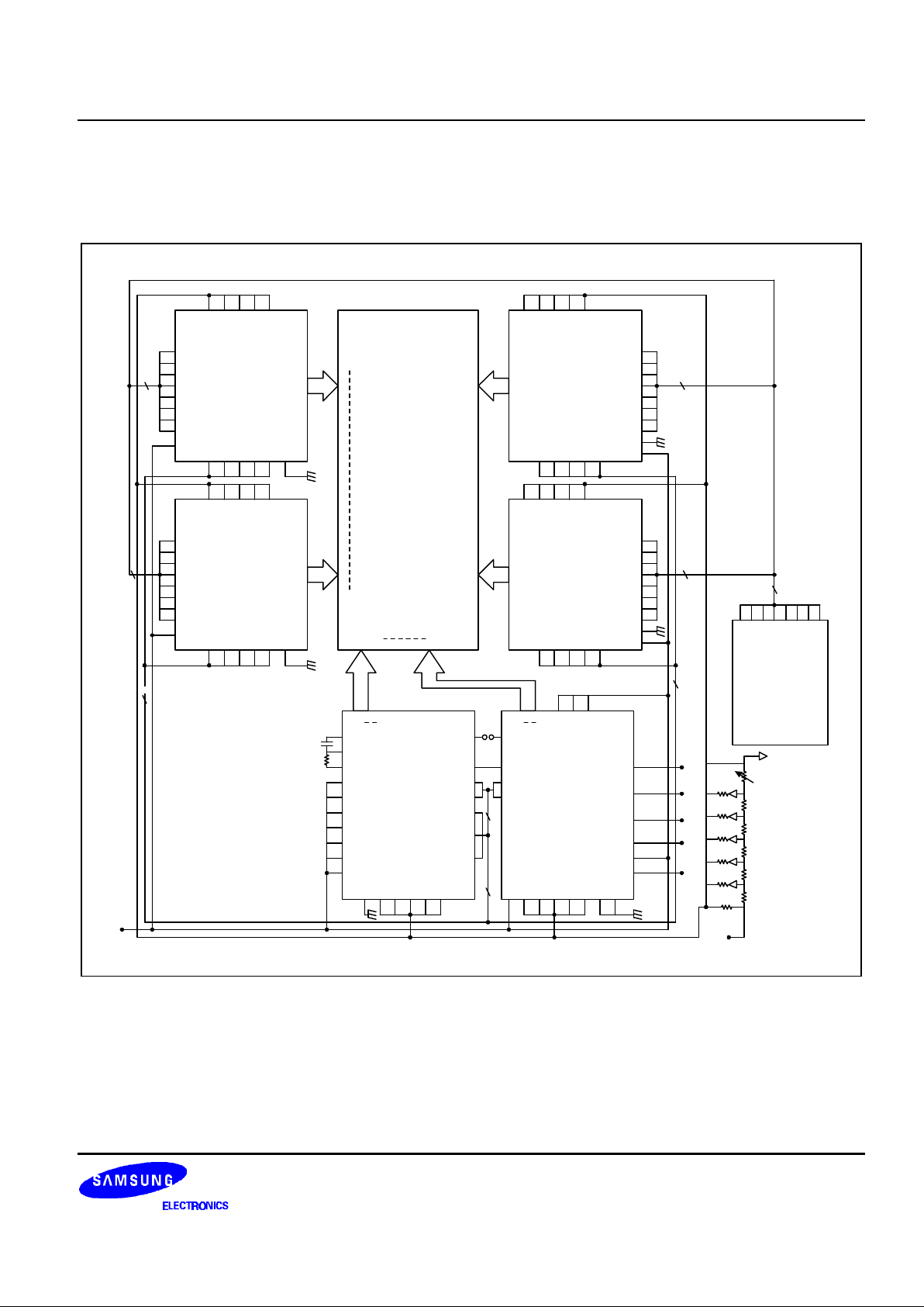
64CH COMMON DRIVER FOR DOT MATRIX LCD S6B0107
1
INTRODUCTION
The S6B0107 (TQFP type: S6B2107) is an LCD driver LSI with 64 channel outputs for dot matrix liquid
crystal graphic display systems. This device provides 64 shift registers and 64 output drivers. It
generates the timing signal to control the S6B0108 (64 channel segment driver – TQFP type: S6B2108).
The S6B0107 is fabricated by low power CMOS high voltage process technology, and is composed of the
liquid crystal display system in combination with the S6B0108 (64 channel segment driver).
FEATURES
• Dot matrix LCD common driver with 64 channel output
• 64-bit shift register at internal LCD driver circuit
• Internal timing generator circuit for dynamic display
• Selection of master/slave mode
• Applicable LCD duty: 1/48, 1/64, 1/96, 1/128
• Power supply voltage: + 5V ± 10%
• LCD driving voltage: 8V - 17V (VDD-VEE)
• Interface
Driver
COMMON SEGMENT
Controller
Other S6B0107 S6B0108 MPU
• High voltage CMOS process
• 100QFP / 100TQFP or bare chip available
Page 2

S6B0107 64CH COMMON DRIVER FOR DOT MATRIX LCD
2
BLOCK DIAGRAM
64 bit 4- Level Driver
64 bit Bi-Directional Shift
Register
Data Shift Direction & Phase
Selection Control Circuit
OSC
C1C2C3
C62
C63
C64
V0L
V1L
V4L
V5L
DIO1
PCLK2
SHL
C
R
M
CL2
DIO2
V5R
Timing Generator
Circuit
CR
FRM
CLK1
CLK2
V
DD
VSSV
EE
DS1
DS2
MS
FS
V4R
V1R
V0R
Page 3

64CH COMMON DRIVER FOR DOT MATRIX LCD S6B0107
3
PIN CONFIGURATION
100 QFP
S6B0107
1
2
3
4
5
6
7
8
9
10
11
12
13
14
15
16
17
18
19
20
21
22
23
24
25
26
27
28
29
30
80
79
78
77
76
75
74
73
72
71
70
69
68
67
66
65
64
63
62
61
60
59
58
57
56
55
54
53
52
51
31323334353637383940414243444546474849
50
100
99989796959493929190898887868584838281
C22
C21
C20
C19
C18
C17
C16
C15
C14
C13
C12
C11
C10
C9
C8
C7
C6
C5
C4
C3
C2
C1
V
EE
V1L
V4L
V5L
V0L
V
DD
DIO1
FS
C23
C24
C25
C26
C27
C28
C29
C30
C31
C32
C33
C34
C35
C36
C37
C38
C39
C40
C41
C42
DS1
DS2
CNCR
NCCRNC
SHL
V
SS
NC
MS
CLK2
CLK1
NC
FRM
M
NC
PCLK2
DIO2
C43
C44
C45
C46
C47
C48
C49
C50
C51
C52
C53
C54
C55
C56
C57
C58
C59
C60
C61
C62
C63
C64
V
EE
V1R
V4R
V5R
V0R
NC
CL2
NC
Page 4

S6B0107 64CH COMMON DRIVER FOR DOT MATRIX LCD
4
PAD DIAGRAM (CHIP LAYOUT FOR THE 100QFP)
28293031323334353637383940414243444546474849505152
53
1
1009998979695949392919089888786858483828180
C22
C23
C24
C25
C26
C27
C28
C29
C30
C31
C32
C33
C34
C35
C36
C37
C38
C39
C40
C41
C42
C43
VDD
DIO1
FS
DS1
DS2
CNCR
NCCRNC
SHL
VSS
NC
MS
CLK2
CLK1
NC
FRM
M
NC
PCLK2
DIO2
NC
CL2
NC
2
3
4
5
6
7
8
9
10
11
12
13
14
15
16
17
18
19
20
21
22
23
24
25
26
27
C21
C20
C19
C18
C17
C16
C15
C14
C13
C12
C11
C10
C9
C8
C7
C6
C5
C4
C3
C2
C1
V
EE
V1L
V4L
V5L
V0L
Chip size: 3450
×
4000
PAD size: 100
×
100
Unit : µm
(0, 0) X
Y
79
78
77
76
75
74
73
72
71
70
69
68
67
66
65
64
63
62
61
60
59
58
57
56
55
54
C44
C45
C46
C47
C48
C49
C50
C51
C52
C53
C54
C55
C56
C57
C58
C59
C60
C61
C62
C63
C64
V
EE
V1R
V4R
V5R
V0R
There is the mark S6B0107 on the center of the chip.
Page 5

64CH COMMON DRIVER FOR DOT MATRIX LCD S6B0107
5
PAD CENTER COORDINATES (100QFP)
Pad
Number
Pad
Name
Coordinate Pad
Number
Pad
Name
Coordinate Pad
Number
Pad
Name
Coordinate
X Y X Y X Y
1 C22 -1314.5 1775.4
32 DS2 -677.6 -1775
71 C52 1500.9 630
2 C21 -1499.9 1630 34 C -527.6 -1775
72 C51 1500.9 755
3 C20 -1499.9 1505 35 R -377.6 -1775
73 C50 1500.9 880
4 C19 -1499.9 1380 37 CR -227.6 -1775
74 C49 1500.9 1005
5 C18 -1499.9 1255 39 SHL -77.6 -1775
75 C48 1500.9 1130
6 C17 -1499.9 1130 40 VSS 113.8 -1775
76 C47 1500.9 1255
7 C16 -1499.9 1005 42 MS 308.7 -1775
77 C46 1500.9 1380
8 C15 -1499.9 880 43 CLK2 458.7 -1775
78 C45 1500.9 1505
9 C14 -1499.9 755 44 CLK1 608.7 -1775
79 C44 1500.9 1630
10 C13 -1499.9 630 46 FRM 758.7 -1775
80 C43 1310.5 1775.4
11 C12 -1499.9 505 47 M 908.7 -1775
81 C42 1185.5 1775.4
12 C11 -1499.9 380 49 PCLK2 1058.7 -1775
82 C41 1060.5 1775.4
13 C10 -1499.9 255 50 DI02 1208.7 -1775
83 C40 935.5 1775.4
14 C9 -1499.9 130 52 CL2 1358.7 -1775
84 C39 810.5 1775.4
15 C8 -1499.9
5 54 V0R 1500.9 -1495
85 C38 685.5 1775.4
16 C7 -1499.9 -120 55 V5R 1500.9 -1370
86 C37 560.5 1775.4
17 C6 -1499.9 -245 56 V4R 1500.9 -1245
87 C36 435.5 1775.4
18 C5 -1499.9 -370 57 V1R 1500.9 -1120
88 C35 310.5 1775.4
19 C4 -1499.9 -495 58 VEE 1500.9 -995 89 C34 185.5 1775.4
20 C3 -1499.9 -620 59 C64 1500.9 -870 90 C33 60.5 1775.4
21 C2 -1499.9 -745 60 C63 1500.9 -745 91 C32 -64.5 1775.4
22 C1 -1499.9 -870 61 C62 1500.9 -620 92 C31 -189.5 1775.4
23 VEE -1499.9 -995 62 C61 1500.9 -495 93 C30 -314.5 1775.4
24 V1L -1499.9 -1120
63 C60 1500.9 -370 94 C29 -439.5 1775.4
25 V4L -1499.9 -1245
64 C59 1500.9 -245 95 C28 -564.5 1775.4
26 V5L -1499.9 -1370
65 C58 1500.9 -120 96 C27 -689.5 1775.4
27 V0L -1499.9 -1495
66 C57 1500.9
5 97 C26 -814.5 1775.4
28 VDD -1345.6 -1775
67 C56 1500.9 130 98 C25 -939.5 1775.4
29 DI01 -1127.6 -1775
68 C55 1500.9 255 99 C24 -1064.5 1775.4
30 FS -977.6 -1775
69 C54 1500.9 380 100 C23 -1189.5 1775.4
31 DS1 -827.6 -1775
70 C53 1500.9 505
Page 6

S6B0107 64CH COMMON DRIVER FOR DOT MATRIX LCD
6
100 TQFP (S6B2107)
C19
C18
C17
C16
C15
C14
C13
C12
C11
C10
C9C8C7C6C5C4C3C2C1
VEE
V1L
V4L
V5L
V0L
VDD
S6B2107
(100 TQFP)
12345678910111213141516171819202122232425
75747372717069686766656463626160595857565554535251
50
49
48
47
46
45
44
43
42
41
40
39
38
37
36
35
34
33
32
31
30
29
28
27
26
76
77
78
79
80
81
82
83
84
85
86
87
88
89
90
91
92
93
94
95
96
97
98
99
100
C44
C43
C42
C41
C40
C39
C38
C37
C36
C35
C34
C33
C32
C31
C30
C29
C28
C27
C26
C25
C24
C23
C22
C21
C20
NC
CL2
NC
DIO2
PCLK2
NC
M
FRM
NC
CLK1
CLK2
MS
NC
VSS
SHL
NC
CR
NC
R
NC
C
DS2
DS1
FS
DIO1
C45
C46
C47
C48
C49
C50
C51
C52
C53
C54
C55
C56
C57
C58
C59
C60
C61
C62
C63
C64
VEE
V1R
V4R
V5R
V0R
Page 7
64CH COMMON DRIVER FOR DOT MATRIX LCD S6B0107
7
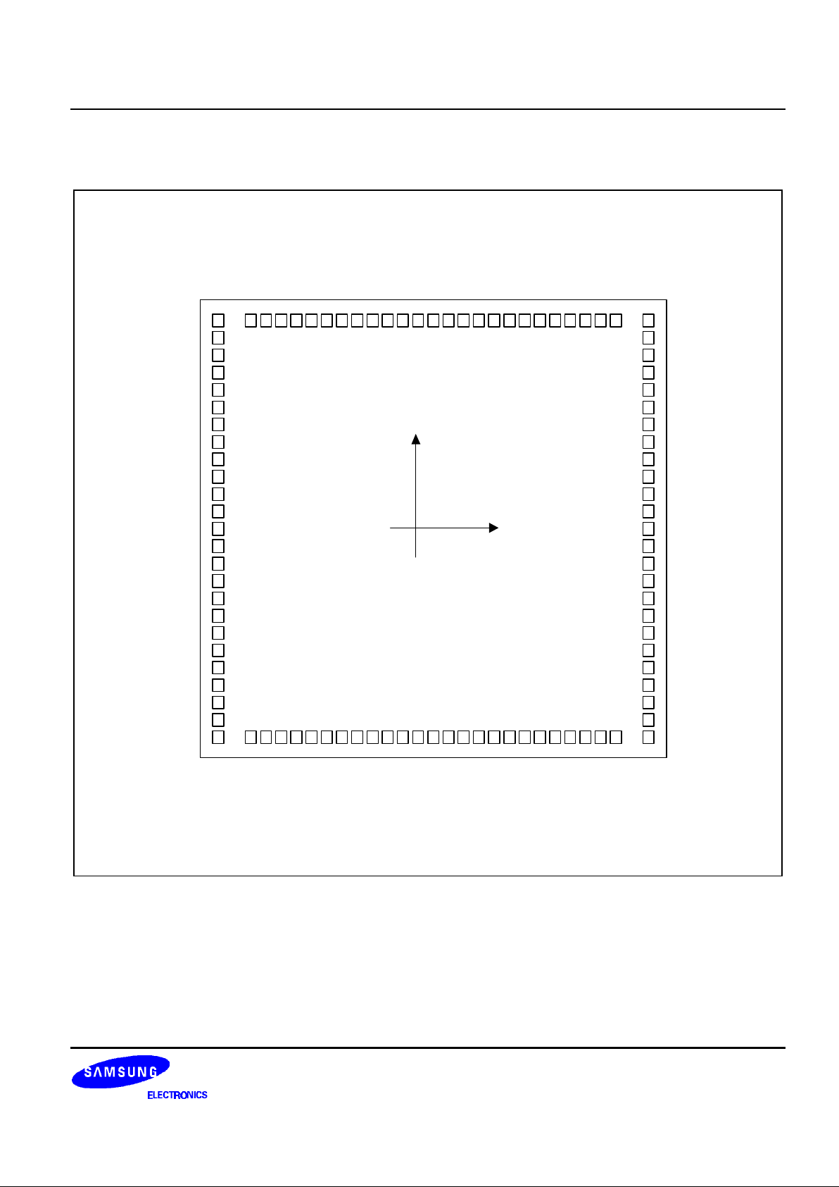
PAD DIAGRAM (CHIP LAYOUT FOR THE 100-TQFP)
75
74
73
72
71
70
69
68
67
66
65
64
63
62
61
60
59
58
57
56
55
54
53
52
51
26272829303132333435363738394041424344454647484950
100999897969594939291908988878685848382818079787776
C20
C21
C22
C23
C24
C25
C26
C27
C28
C29
C30
C31
C32
C33
C34
C35
C36
C37
C38
C39
C40
C41
C42
C43
C44
DIO1
FS
DS1
DS2
CNCR
NCCRNC
SHL
V
SS
NC
MS
CLK2
CLK1
NC
FRM
M
NC
PCLK2
DIO2
NC
CL2
NC
C45
C46
C47
C48
C49
C50
C51
C52
C53
C54
C55
C56
C57
C58
C59
C60
C61
C62
C63
C64
V
EE
V1R
V4R
V5R
V0R
1
2
3
4
5
6
7
8
9
10
11
12
13
14
15
16
17
18
19
20
21
22
23
24
25
C19
C18
C17
C16
C15
C14
C13
C12
C11
C10
C9
C8
C7
C6
C5
C4
C3
C2
C1
V
EE
V1L
V4L
V5L
V0L
V
DD
Chip size: 3850 X 100
PAD size: 100 X 100
Unit : µm
(0, 0) X
Y
There is the mark S6B2107 on the center of the chip.
Page 8
S6B0107 64CH COMMON DRIVER FOR DOT MATRIX LCD
8
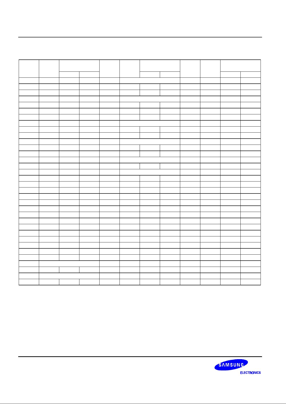
PAD CENTER COORDINATES (100-TQFP)
Pad
Number
Pad
Name
Coordinate Pad
Number
Pad
Name
Coordinate Pad
Number
Pad
Name
Coordinate
X Y X Y X Y
1 C19 -1697 1534
35 NC 69 C51 1697 784
2 C18 -1697 1409
36 SHL -195 -1821
70 C50 1697
909
3 C17 -1697 1284
37 VSS 0 -1821
71 C49 1697 1034
4 C16 -1697 1159
38 NC 72 C48 1697 1159
5 C15 -1697 1034
39 MS 195 -1821
73 C47 1697 1284
6 C14 -1697 909 40 CLK2
345 -1821
74 C46 1697 1409
7 C13 -1697 784 41 CLK1 495 -1821
75 C45 1697 1534
8 C12 -1697 659 42 NC 76 C44 1500 1822
9 C11 -1697 534 43 FRM 645 -1821
77 C43 1375 1822
10 C10 -1697 409 44 M 795 -1821
78 C42 1250 1822
11 C9 -1697 284 45 NC 79 C41 1125 1822
12 C8 -1697 159 46 PCLK2 945 -1821
80 C40 1000 1822
13 C7 -1697
34 47 DIO2 1095 -1821
81 C39 875 1822
14 C6 -1697 -91 48 NC 82 C38 750 1822
15 C5 -1697 -216 49 CL2 1245 -1821
83 C37 625 1822
16 C4 -1697 -341 50 NC 84 C36 500 1822
17 C3 -1697 -466 51 V0R 1697 -1466
85 C35 375 1822
18 C2 -1697 -591 52 V5R 1697 -1341
86 C34 250 1822
19 C1 -1697 -716 53 V4R 1697 -1216
87 C33 125 1822
20 VEE -1697 -841 54 V1R 1697 -1091
88 C32 0 1822
21 V1L -1697 -966 55 VEE 1697 -966 89 C31 -125 1822
22 V4L -1697 -1091
56 C64 1697 -841 90 C30 -250 1822
23 V5L -1697 -1216
57 C63 1697 -716 91 C29 -375 1822
24 V0L -1697 -1341
58 C62 1697 -591 92 C28 -500 1822
25 VDD -1697 -1466
59 C61 1697 466 93 C27 -625 1822
26 DIO1 -1245 -1821
60 C60 1697 -341 94 C26 -750 1822
27 FS -1095 -1821
61 C59 1697 -216 95 C25 -875 1822
28 DS1 -945 -1821
62 C58 1697
-91 96 C24 -1000 1822
29 DS2 -795 -1821
63 C57 1697
34 97 C23 -1125 1822
30 C -645 -1821
64 C56 1697 159 98 C22 -1250 1822
31 NC 65 C55 1697
284 99 C21 -1375 1822
32 R -495 -1821
66 C54 1697 409 100 C20 -1500 1822
33 NC 67 C53 1697
534
34 CR -345 -1821
68 C52 1697 659
Page 9
64CH COMMON DRIVER FOR DOT MATRIX LCD S6B0107
9
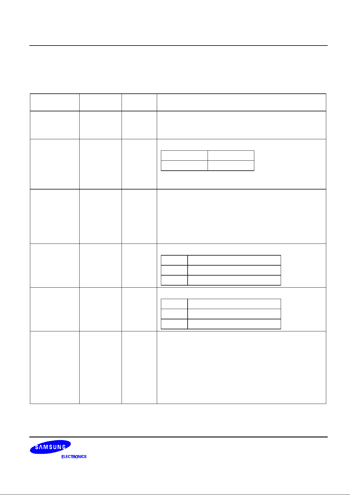
PIN DESCRIPTION
Table 1. Pin Description
Pin Number
QFP (TQFP)
Symbol I/O Description
28(25)
40(37)
23(20), 58(55)
V
DD
V
SS
VEE
Power
For internal logic circuit (+5V ± 10%)
GND ( = 0 V)
For LCD driver circuit
27(24), 54(51)
24(21), 57(54)
25(22), 56(53)
26(23), 55(52)
V0L, V0R
V1L, V1R
V4L, V4R
V5L, V5R
Power Bias supply voltage terminals to drive LCD.
Slelect Level
V0L (R), V5L (R)
Non-Select Level
V1L (R), V4L (R)
V0L and V0R (V1L & V1R, V4L & V4R, V5L & V5R) should
be connected by the same voltage.
42(39) MS Input Selection of master/slave mode
- Master mode (MS = 1)
DIO1, DIO2, CL2 and M is output state.
- Slave mode (MS = 0)
SHL = 1 → DIO1 is input state (DIO2 is output state)
SHL = 0 → DIO2 is input state (DIO1 is output state)
CL2 and M are input state.
39(36) SHL Input Selection of data shift direction.
SHL
H
L
Data Shift Direction
DIO1 → C1 ...... C64 → DIO2
DIO2 → C64 ...... C1 → DIO1
49(46) PCLK2 Input Selection of shift clock (CL2) phase.
PCLK2
H
L
Shift Clock (CL2) Phase
Data shift at the rising edge of CL2
Data shift at the falling edge of CL2
30(27) FS Input Selection of oscillation frequency.
- Master mode
When the frame frequency is 70 Hz, the oscillation
frequency
should be
fosc = 430kHz at FS = 1(VDD)
fosc = 215kHz at FS = 0(VSS)
- Slave mode
Connect to VDD.
Page 10
S6B0107 64CH COMMON DRIVER FOR DOT MATRIX LCD
10
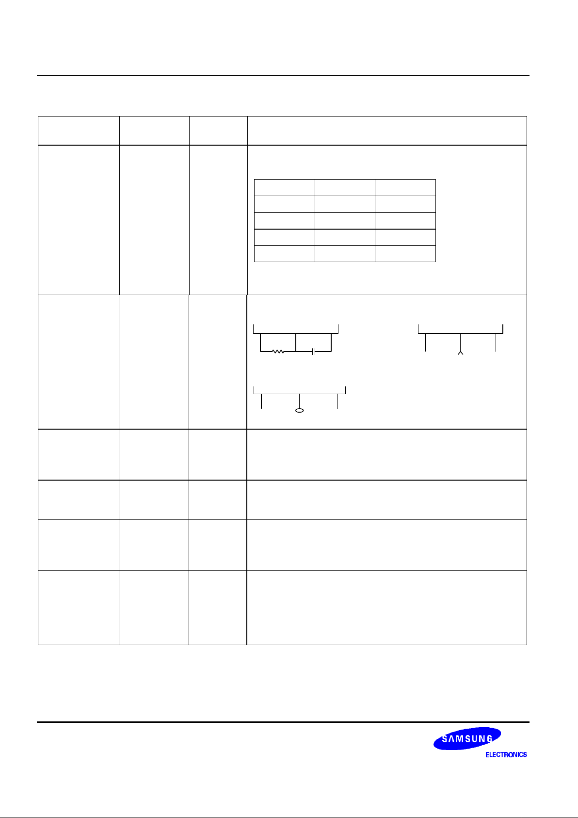
Table 1. Pin Description (Continued)
Pin Number
QFP (TQFP)
Symbol I/O Description
31(28)
32(29)
DS1
DS2
Input Selection of display duty.
- Master mode
DS1
L
DS2
L
L
H
H
L
Duty
1/48
1/64
1/96
H H 1/128
- Slave mode
Connect to VDD
33(30)
35(32)
37(34)
C
R
CR
RC Oscillator
- Master mode: Use these terminals as shown below.
S6B0107
R C
R
f
CR
C
f
S6B0107
R CCR
Open Open
External
- Slave mode: Stop the oscillator as shown below.
R CCR
Open Open
V
DD
44(41)
43(40)
CLK1
CLK2
Output Operating clock output for the S6B0108
- Master mode: connection to CLK1 and CLK2 of the
S6B0108
- Slave mode: open
46(43) FRM Output Synchronous frame signal.
- Master mode: connection to FRM of the S6B0108
- Slave mode: open
47(44) M Input/
Output
Alternating signal input for LCD driving.
- Master mode: output state Connection to M of the
S6B0108
- Slave mode: input state Connection to the controller
52(49) CL2 Input /
Output
Data shift clock
- Master mode: output state Connection to CL of the
S6B0108
- Slave mode: input state Connection to shift clock
terminal of
the controller.
Page 11
64CH COMMON DRIVER FOR DOT MATRIX LCD S6B0107
11
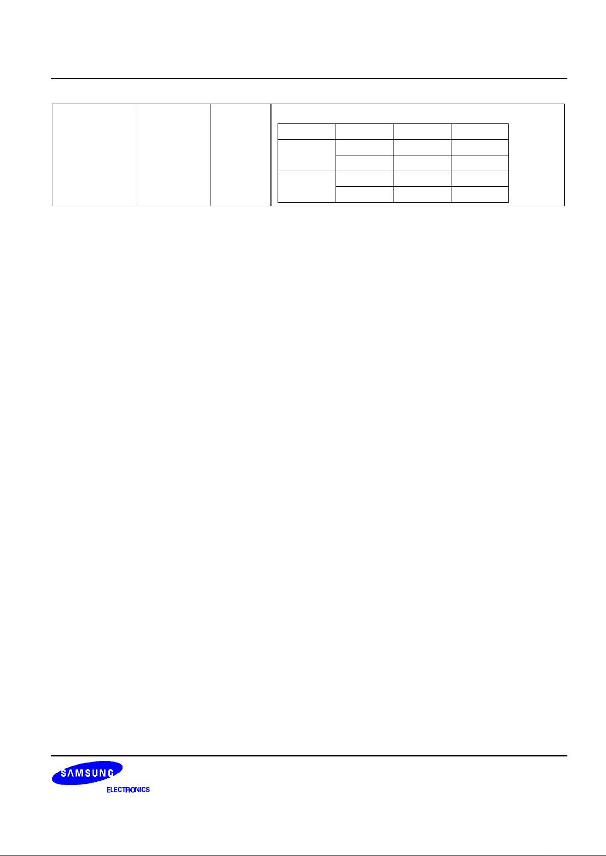
29(26)
50(47)
DIO1
DIO2
Input/
Output
Data input/output pin of internal shift register.
MS
H
DS2
H
L
L
L
DIO1
Output
Output
InputH
Output
DIO2
Output
Output
Output
Input
Page 12
S6B0107 64CH COMMON DRIVER FOR DOT MATRIX LCD
12
Table 1. Pin Description (Continued)
Pin Number
QFP (TQFP)
Symbol I/O Description
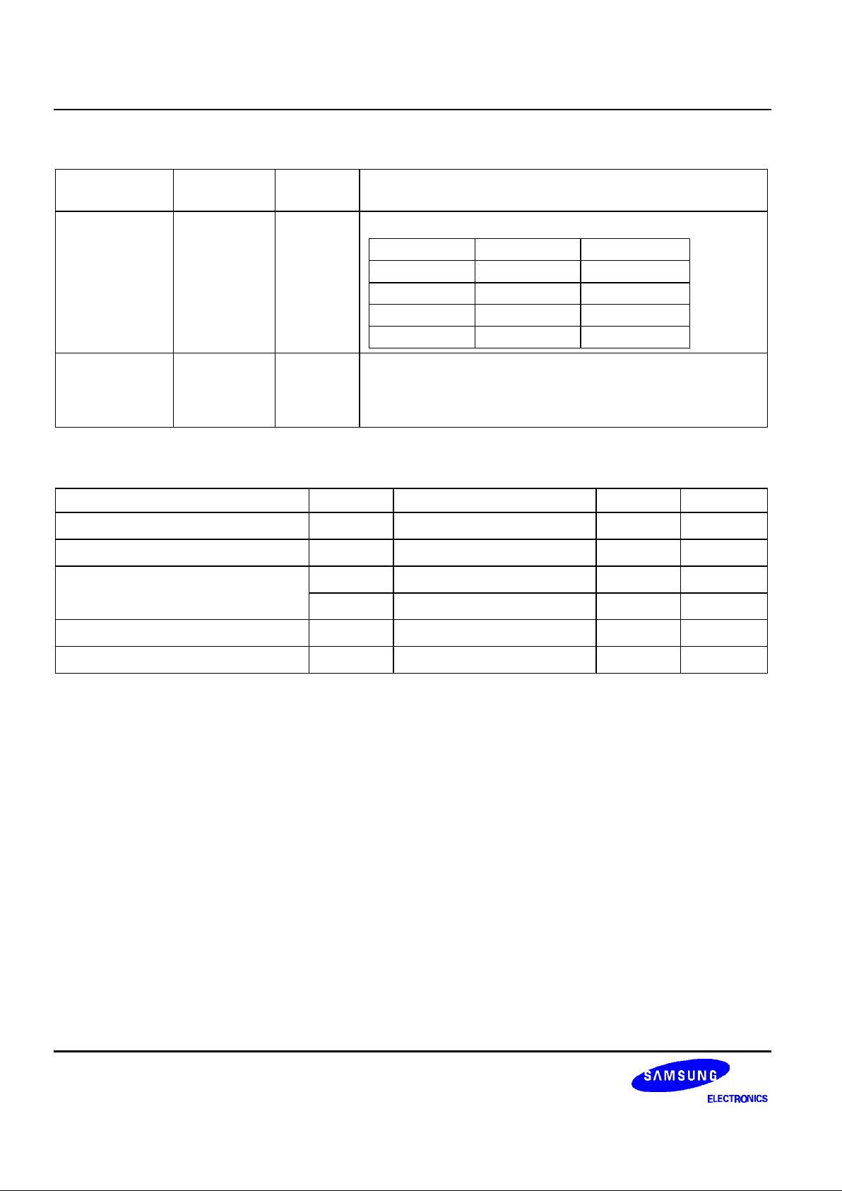
22-1(19-1)
100-59(100-
56)
C1-C64 Output Common signal output for LCD driving.
Data
L
L
H
H
M Out
L
H
L
H
V
1
V
4
V
5
V
0
34(31), 36(33)
38(35), 41(38)
45(42), 48(45)
51(48), 53(50)
NC No connection
MAXIMUM ABSOLUTE LIMIT
Characteristic Symbol Value Unit Note
Operating voltage
VDD
-0.3 to +7.0 V
(1)
Supply voltage
VEE VDD-19.0 to VDD+0.3
V
(4)
Driver supply voltage
VB -0.3 to VDD+0.3
V
(1), (2)
V
LCD
VEE-0.3 to VDD+0.3
V
(3), (4)
Operating temperature
T
OPR
-30 to +85
°C
-
Storage temperature
T
STG
-55 to +125
°C
-
NOTES:
1. Based on V
SS
= 0V
2. Applies to input terminals and I/O terminals at high impedance. (Except V0L(R), V1L(R), V4L(R) and V5L(R))
3. Applies to V0L(R), V1L(R), V4L(R) and V5L(R).
4. Voltage level: V
DD
≥ V0L = V0R ≥ V1L = V1R ≥ V4L = V4R ≥ V5L = V5R ≥ VEE.
Page 13
64CH COMMON DRIVER FOR DOT MATRIX LCD S6B0107
13
ELECTRICAL CHARACTERISTICS
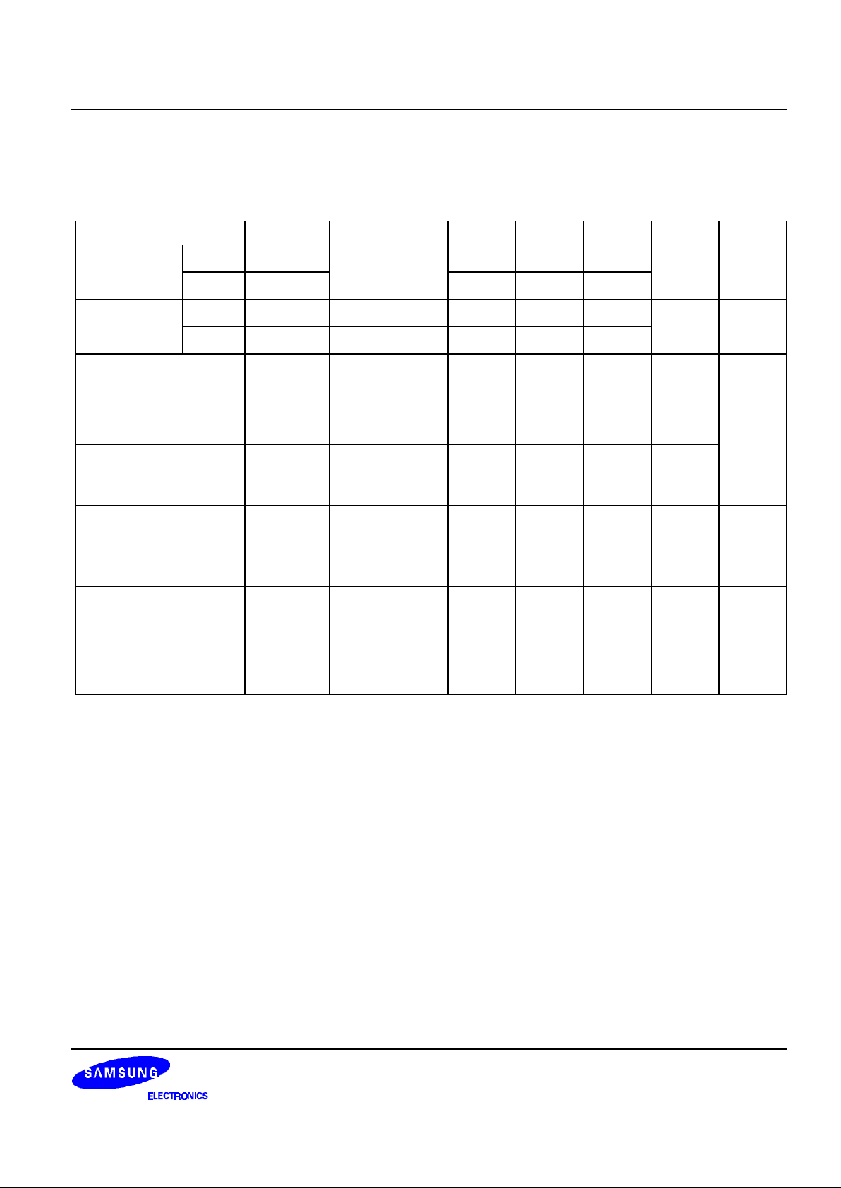
DC CHARACTERISTICS (VDD = +5V ± 10%, VSS = 0V, |VDD-VEE |=8 - 17V, TA = -30 - +85°C)
Characteristic Symbol Condition Min Typ Max Unit Note
High
VIH
-
0.7V
DD
-
VDD
V
(1)
Input Voltage
Low
VIL
VSS
-
0.3V
DD
High
VOH I
OH
= -0.4mA VDD-0.4
- - V
(2)
Output
voltage
Low
VOL I
OL
= 0.4mA
- - 0.4
Input leakage current
I
LKG
V
IN
= VDD-VSS
-1.0 - 1.0 µA
(1)
OSC frequency
f
OSC
Rf = 47kΩ ±
2%
Cf = 20pf ± 5%
315 450 585 kHz
On resistance (VDIVCi)
RON
VDD-V
EE
= 17V
Load current =
± 150µA
- - 1.5 KΩ
Operating current
I
DD1
Master mode
1/128 Duty
- - 1.0 mA
(3)
I
DD2
Slave mode
1/128 Duty
- - 200 µA
(4)
Supply current
IEE
Master mode
1/128 Duty
- - 100
(5)
Operating
f
op1
Master mode
External clock
50 - 600 kHz
Frequency
f
op2
Slave mode 0.5 - 1500
NOTES:
1. Applies to input terminals FS, DS1, DS2, CR, SHL, MS and PCLK2 and I/O terminals DIO1, DIO2, M and CL2 in
the
input state.
2. Applies to output terminals CLK1, CLK2 and FRM and I/O terminals DIO1, DIO2, M and CL2 in the output
state.
3. This value is specified at about the current flowing through VSS. Internal oscillation circuit: Rf = 47kΩ, Cf =
20pF. Each
terminal of DS1, DS2, FS, SHL and MS is connected to VDD and out is no load.
4. This value is specified at about the current flowing through VSS. Each terminal of DS1, DS2, FS, SHL, PCLK2
and CR is
connected to VDD, and MS is connected to V
SS
.
CL2, M, DIO1 is external clock.
5. This value is specified at about the current flowing through VEE. Don’t connect to V
LCD
(V1-V5).
Page 14
S6B0107 64CH COMMON DRIVER FOR DOT MATRIX LCD
14
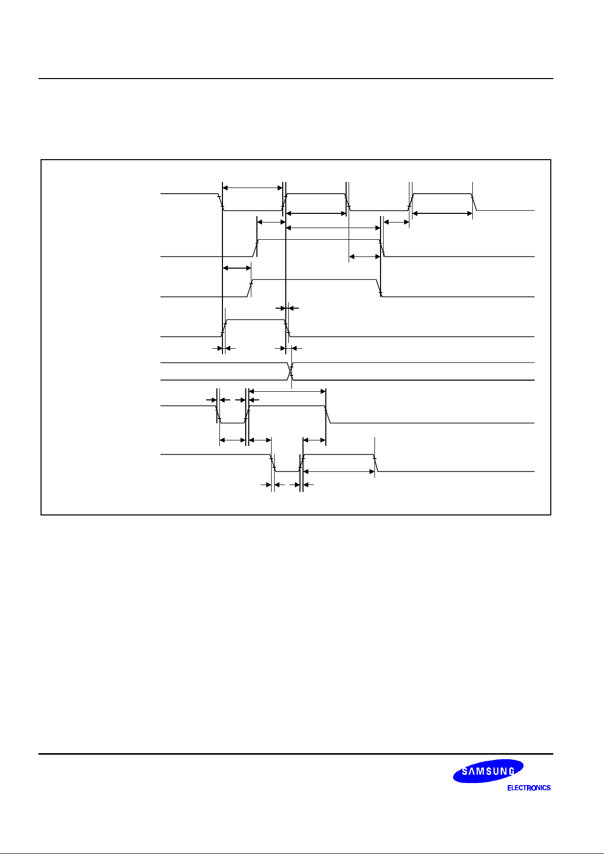
AC CHARACTERISTICS (VDD = 5V ± 10%, TA = -30°C - +85°C)
Master Mode (MS = VDD, PCLK2 = VDD, Cf = 20pF, Rf = 47kΩ)
CL2
DIO1 (SHL = VDD)
DIO2 (SHL = VSS)
CLK1
t
su
t
su
t
D
DIO2 (SHL = VDD)
DIO1 (SHL = VSS)
FRM
M
CLK2
0.7V
DD
0.3V
DD
0.7V
DD
0.3V
DD
t
WLC
t
WHC
t
DF
t
DM
t
DM
t
F
t
R
t
WH1
t
D12
t
WL1
t
D21
t
F
t
R
t
WH2
t
D
t
DH
t
WHC
Page 15
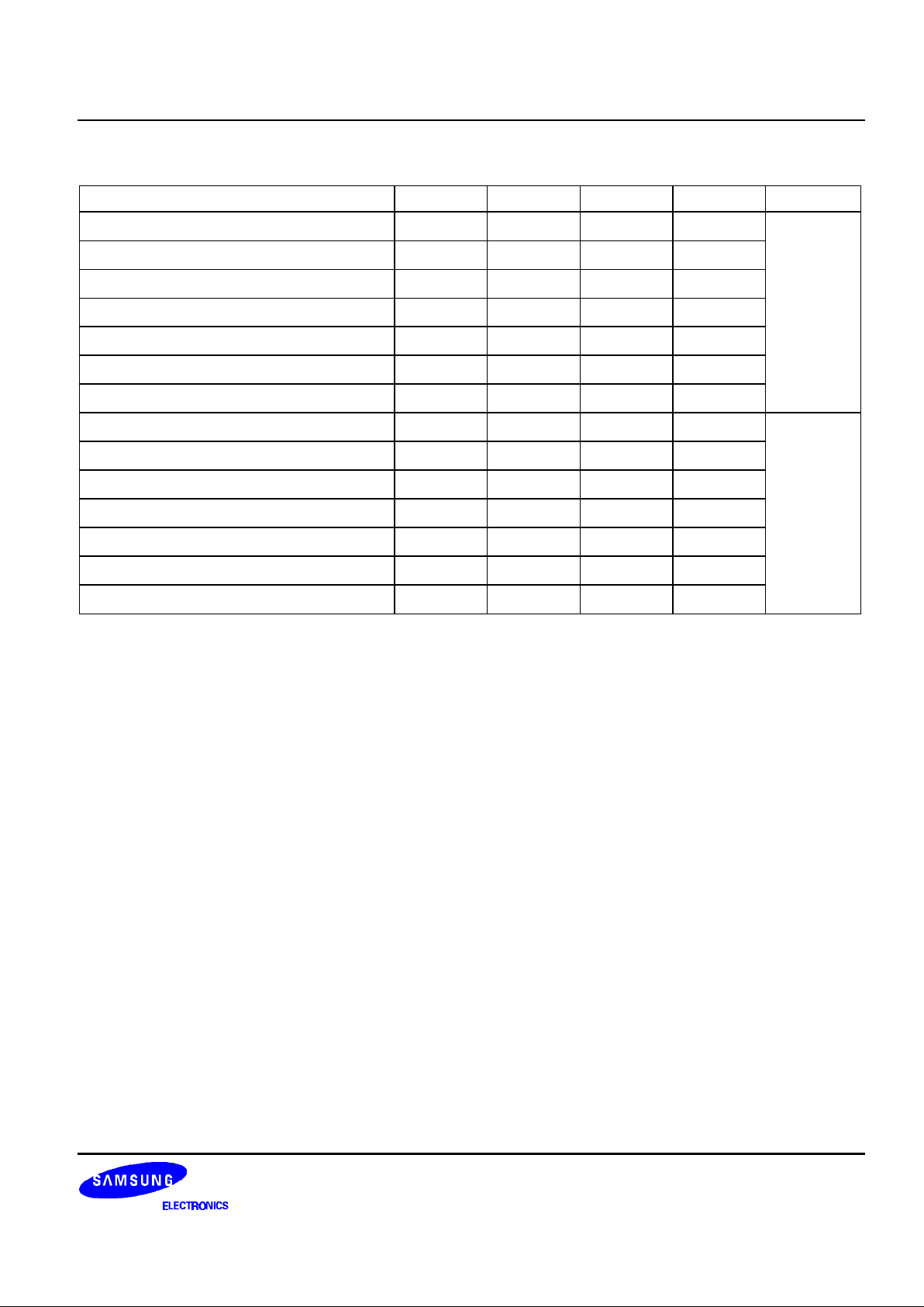
64CH COMMON DRIVER FOR DOT MATRIX LCD S6B0107
15
Master Mode
Characteristic Symbol Min Typ Max Unit
Data setup time
tSU
20 - - µs
Data hold time
tDH
40 - -
Data delay time
tD
5 - -
FRM delay time
tDF
-2 - 2
M delay time
tDM
-2 - 2
CL2 low level width
t
WLC
35 - -
CL2 high level width
t
WHC
35 - -
CLK1 low level width
t
WL1
700 - - ns
CLK2 low level width
t
WL2
700 - -
CLK1 high level width
t
WH1
2100 - -
CLK2 high level width
t
WH2
2100 - -
CLK1-CLK2 phase difference
t
D12
700 - -
CLK2-CLK1 phase difference
t
D21
700 - -
CLK1, CLK2 rise/fall time
t
R
/
tF
- - 150
Page 16
S6B0107 64CH COMMON DRIVER FOR DOT MATRIX LCD
16
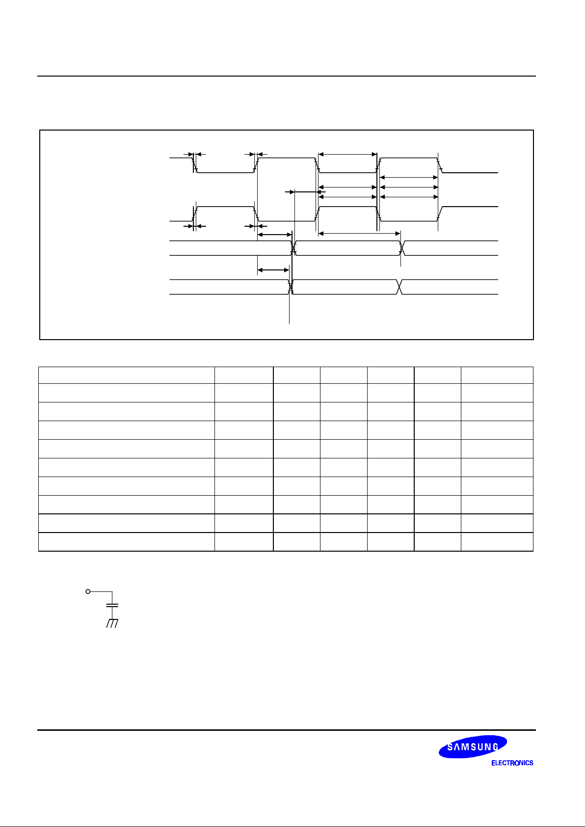
Slave Mode (MS = VSS)
t
WLC
t
WHC1
CL2 (PLK2 = V
SS
)
CL2 (PLK2 = V
DD
)
DIO1 (SHL = V
DD
)
DIO2 (SHL = V
SS
)
Input Data
DIO1 (SHL = V
DD
)
DIO2 (SHL = V
SS
)
Onput Data
t
F
t
R
t
WLC1
0.7V
DD
0.3V
DD
0.7V
DD
0.3V
DD
0.7V
DD
0.3V
DD
t
WHC2
t
SU
t
R
t
F
t
D
t
HCL
t
H
Characteristics Symbol Min Typ Max Unit Note
CL2 low level width
t
WLC1
450 - - ns
PCLK2 = V
SS
CL2 high level width
t
WHC1
150 - - ns
PCLK2 = V
SS
CL2 low level width
t
WLC2
150 - - ns
PCLK2 = V
DD
CL2 high level width
t
WHL
450 - - ns
PCLK2 = V
DD
Data setup time
tSU
100 - - ns
Data hold time
tDH
100 - - ns
Data delay time
tD
- - 200 ns
(NOTE)
Output data hold time
tH
10 - - ns
CL2 rise/fall time
tR/tF
- - 30 ns
NOTE: Connect load CL = 30pF
Output
30pF
Page 17
64CH COMMON DRIVER FOR DOT MATRIX LCD S6B0107
17
FUNCTIONAL DESCRIPTION
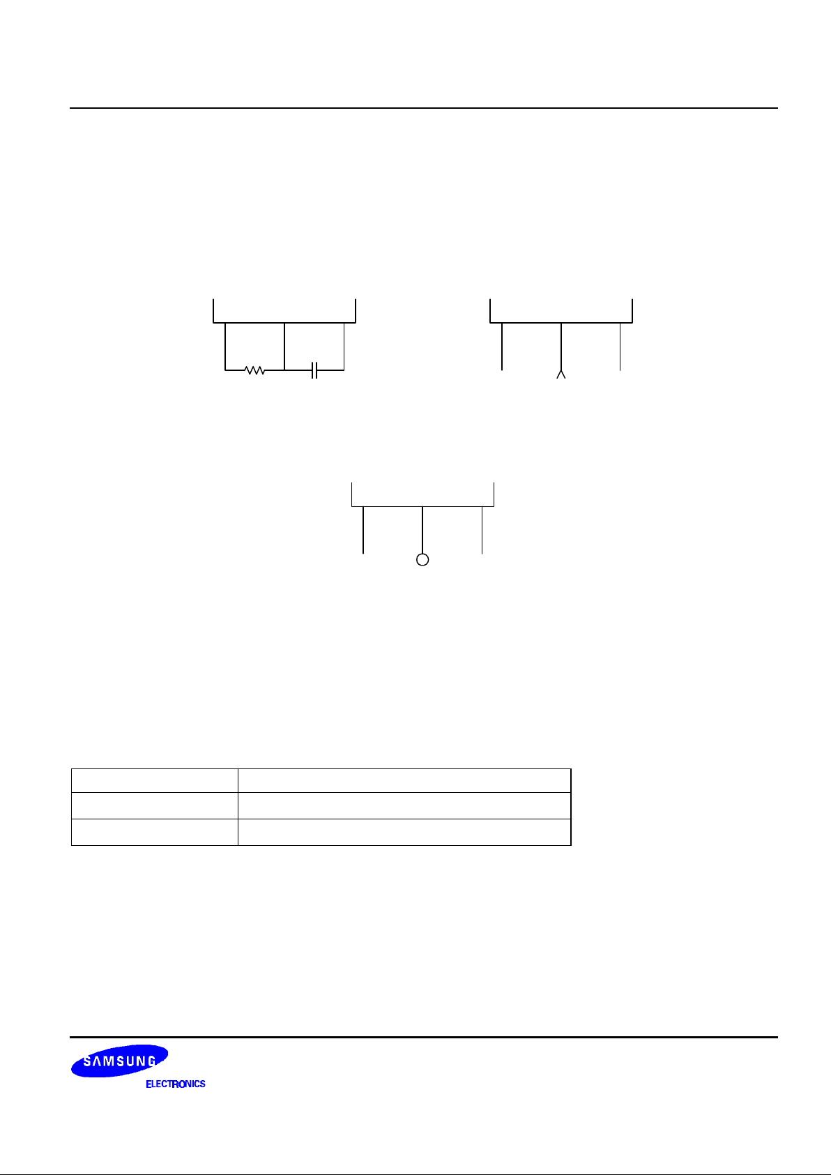
RC Oscillator
The RC Oscillator generates CL2, M, FRM of the S6B0107, and CLK1 and CLK2 of the S6B0108 by the
oscillation resister R and capacitor C. When selecting the master/slave mode, the oscillation circuit is as
following:
Master Mode: In the master mode, use these terminals as shown below.
S6B0107
R C
R
f
CR
C
f
47K
Ω
20pF
Internal Oscillation
S6B0107
R CCR
Open Open
External Clock
External
Clock
Slave Mode: In the slave mode, stop the oscillator as shown below.
S6B0107
R CCR
Open Open
V
DD
Timing Generation Circuit
It generates CL2, M, FRM, CLK1 and CLK2 by the frequency from the oscillation circuit.
Selection of Master/Slave (M/S) Mode
- When M/S is H, it generates CL2, M, FRM, CLK1 and CLK2 internally.
- When M/S is “L”, it operates by receiving M and CL2 from the master device.
Frequency Selection (FS)
To adjust FRM frequency by 70Hz, the oscillation frequency should be as follows:
FS Oscillation Frequency
H
f
OSC
= 430kHz
L
f
OSC
= 215kHz
In the slave mode, it is connected to VDD.
Page 18
S6B0107 64CH COMMON DRIVER FOR DOT MATRIX LCD
18
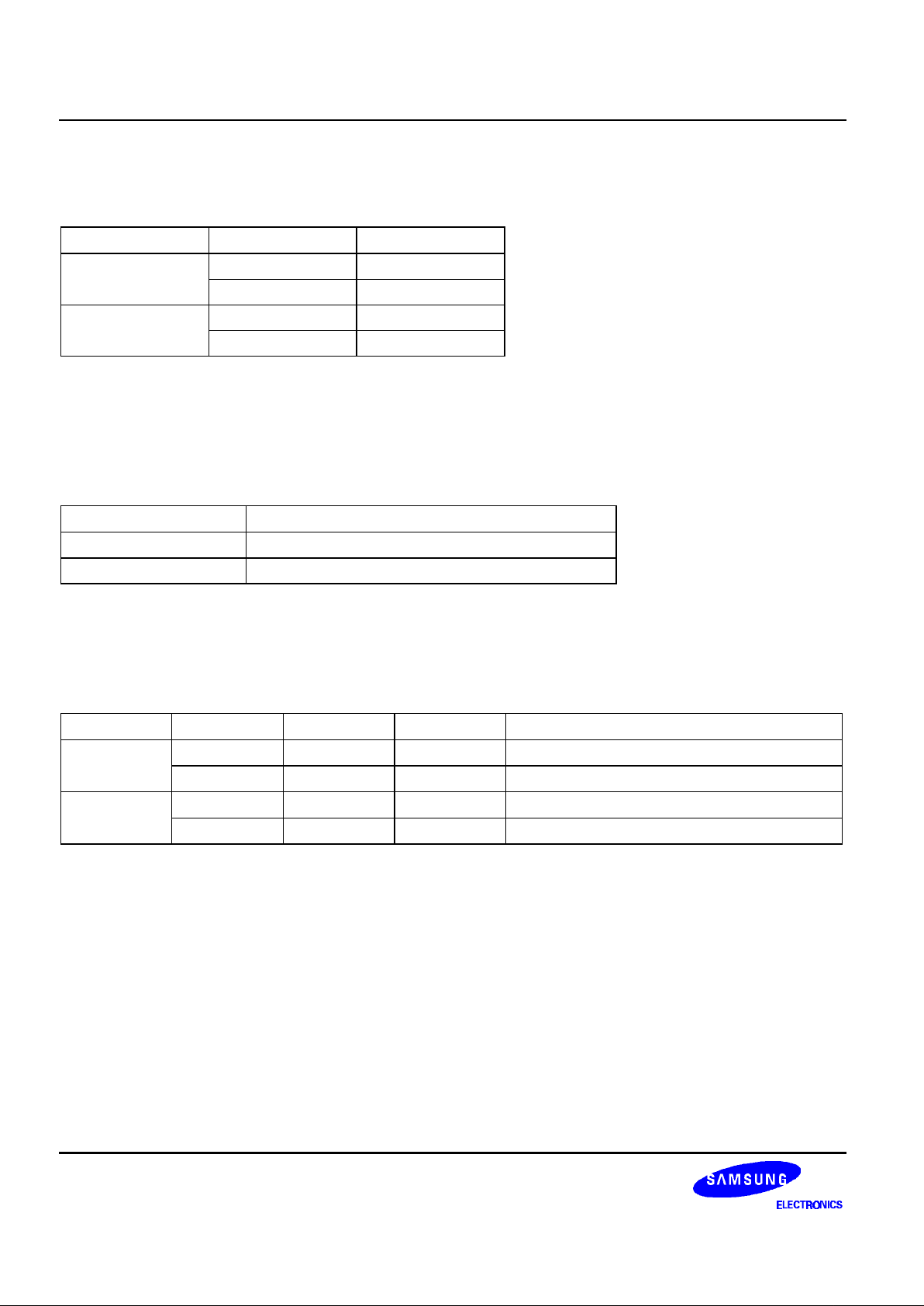
Duty Selection (DS1, DS2)
It provides various duty selections according to DS1 and DS2.
DS1 DS2 DUTY
L L 1/48
H 1/64
H L 1/96
H 1/128
Data Shift & Phase Select Control
Phase Selection
It is a circuit to shift data on synchronization or rising edge, or falling edge of the CL2 according to
PCLK2.
PCLK2 Phase Selection
H Data shift on rising edge of CL2
L Data shift on falling edge of CL2
Data Shift Direction Selection
When M/S is connected to VDD, DIO1 and DIO2 terminal is only output.
When M/S is connected to VSS, it depends on the SHL.
MS SHL DIO1 DIO2 Direction of Data
H H Output Output
C1 → C64
L Output Output
C64 → C1
L H Input Output
DIO1 → C1 → C64 → DIO2
L Output Input
DIO2 → C64 → C1 → DIO1
Page 19
64CH COMMON DRIVER FOR DOT MATRIX LCD S6B0107
19
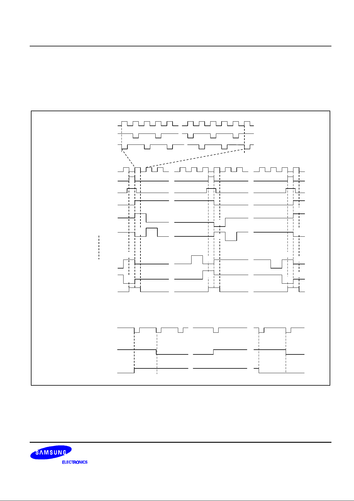
TIMING DIAGRAM
1/48 DUTY TIMING (MASTER MODE)
Condition: DS1 = L, DS2 = L, SHL = H(L), PCLK2 = H
Relation of CL2 & DIO1 ( DIO2 )
C
CLK1
CLK2
CL2
FRM
DIO1 ( DIO2 )
M
C1 ( C48 )
C2 ( C47 )
C47 ( C2 )
C48 ( C1 )
DIO2 ( DIO1 )
CLK2
CL2
DIO1 ( DIO2 )
1 2 3 63 64
1
2
3
46 47 48 1 2 3 46 47 48
V0
V4
V0
V1
~
~
~
~
~
~
~
~
~
~
~
~
~
~
~
~
~
~
~
~
~
~
~
~
~
~
~
~
~
~
~
~
~
~
~
~
~
~
~
~
~
~
~
~
~
~
~
~
~
~
~
~
~
~
V1
V4
V4
V5
V1
V1
V5V1
V4
V0
V4
V4
V0
V4
V4
V1
V1
V4
V1
V5
V5
V1
V1
V5
V5
V0
Page 20
S6B0107 64CH COMMON DRIVER FOR DOT MATRIX LCD
20
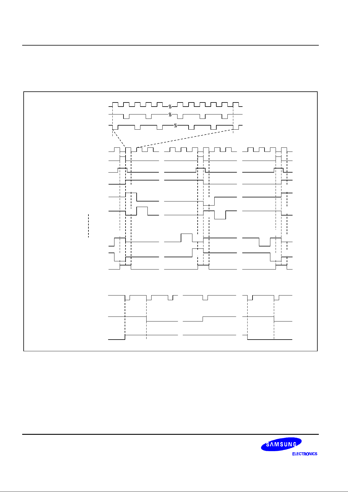
1/128 DUTY TIMING (MASTER MODE)
Condition: DS1 = H, DS2 = H, SHL = H(L), PCLK2 = H
Relation of CL2 & DIO1 ( DIO2 )
C
CLK1
CLK2
CL2
FRM
DIO1 ( DIO2 )
M
C1 ( C128 )
C2 ( C127 )
C127 ( C2 )
C128 ( C1 )
DIO2 ( DIO1 )
CLK2
CL2
DIO1 (DIO2)
1 2 3 23 24
1
2
3
126 127 128 1 2 3 126 127 128
~
~
~
~
~
~
~
~
~
~
~
~
~
~
~
~
~
~
~
~
~
~
~
~
~
~
~
~
~
~
~
~
~
~
~
~
~
~
~
~
~
~
~
~
~
~
~
~
V4
V0
V4
V4
V5
V5
V1
V1
V1
V1
V1
V5V1
V5
V0
V4
V0
V4
V4
V0
V5
V1
V5
V1
V4
V4
V1
V1
V0
V4
Page 21
64CH COMMON DRIVER FOR DOT MATRIX LCD S6B0107
21
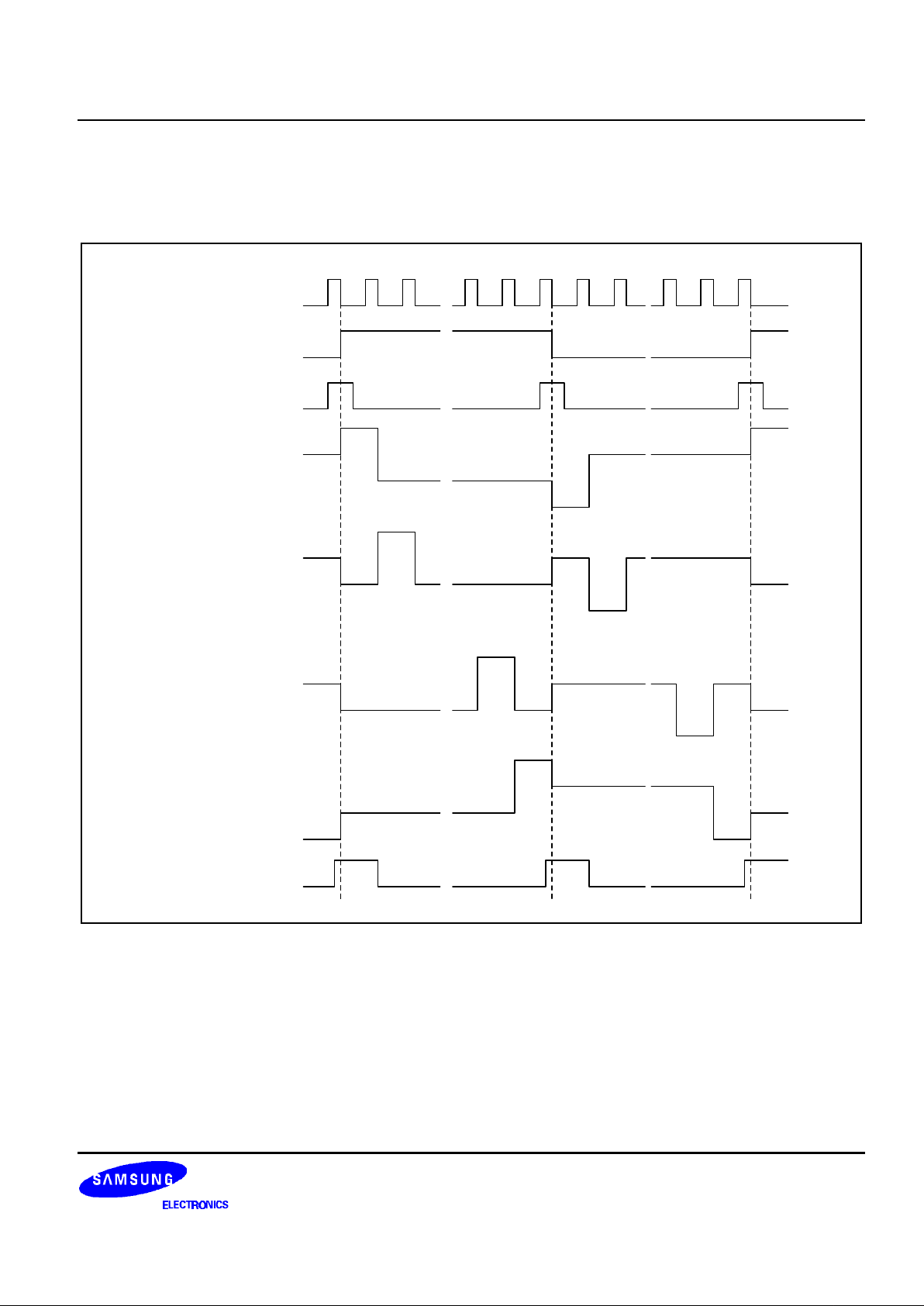
1/48 DUTY TIMING (SLAVE MODE)
Condition: PCLK2 = L, SHL = H(L)
1 2 46 47 48 1 2 46 47 48
CL2
M
DIO1 ( DIO2 )
C1 ( C48 )
C2 ( C47 )
C47 ( C2 )
C48 ( C1 )
DIO2 ( DIO1 )
~
~
~
~
~
~
~
~
~
~
~
~
~
~
~
~
~
~
~
~
~
~
~
~
~
~
~
~
~
~
~
~
V1
V0
V1
V4
V0
V1
V4
V5
V4
V4
V4
V5
V1
V5
V1
V1
V0
V4
V0
V1
V1
V5
V1
V5
V4
V4
V4V4
V0
Page 22
S6B0107 64CH COMMON DRIVER FOR DOT MATRIX LCD
22
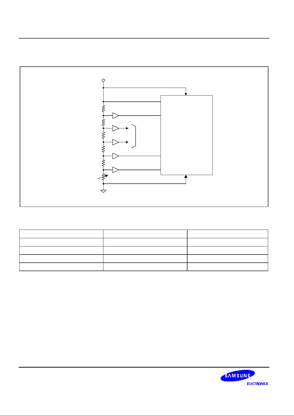
POWER DRIVER CIRCUIT
To
S6B0108
V0
V1
V2
V3
V4
V5
V
DD
R1
R1
R2
R1
R1
VR
V0L/R
V1L/R
V4L/R
V5L/R
V
EE
S6B0107
V
DD
V
EE
Relation of Duty & Bias
Duty Bias RDIV
1/48 1/8 R2 = 4R1
1/64 1/9 R2 = 5R1
1/96 1/11 R2 = 7R1
1/128 1/12 R2 = 8R1
When duty factor is 1/48, the value of R1 & R2 should satisfy.
R1/(4R1 + R2) = 1/8
R1 + 3kΩ, R2 = 12kΩ
Page 23
64CH COMMON DRIVER FOR DOT MATRIX LCD S6B0107
23
APPLICATION CIRCUIT
1/128 duty Segment driver (S6B0108) interface circuit
LCD Panel
V0R/L
V2R/L
V3R/L
V5R/L
CS3
CS2B
CS1B
DB0 -DB7
RSTB
E
R/W
RS
FRM
CLK1
CLK2
M
V
DD
CL
V
SS
V0R/L
V2R/L
V3R/L
V5R/L
V
EE
CS3
CS2B
CS1B
DB0 -DB7
RSTB
E
R/W
RS
FRM
CLK1
CLK2
M
V
DD
CL
V
SS
S6B0108
S6B0108
S
1
- S
64
S
1
- S
64
15
15
SEG128SEG1
COM1 COM128
V
EE
V2R/L
V3R/L
CS3
CS2B
CS1B
DB0 -DB7
RSTB
E
R/W
RS
FRM
CLK1
CLK2MVDDCL
V
SS
S6B0108
S
1
- S
64
V
EE
V0R/L
V5R/L
V
EE
V2R/L
V3R/L
CS3
CS2B
CS1B
DB0 -DB7
RSTB
E
R/W
RS
FRM
CLK1
CLK2MVDDCL
V
SS
S6B0108
S
1
- S
64
V0R/L
V5R/L
MPU
RS
R/W
E
RSTB
DB0 - DB7
CS1B
CS2B
CS3
15
15
15
C1
C64
C
CR
R
DS1
DS2
PCLK2
MS
FS
SHL
V
DD
VSSV
0R/LV1R/LV4R/LV5R/LVEE
DIO2
DIO1
CL2
M
CLK2
CLK1
FRM
C1
C64
V
DD
V
SS
V
0R/LV1R/LV4R/LV5R/LVEE
CLK2
CLK1
FRM
C
PCLK2
FS
DS1
KS2
SHL
CR
R
DIO2
M
CL2
MS
S6B0107
(master)
S6B0107
(slave)
2
5
5
C
1
R
1
open
open
5
openopenopenopenopen
V
DD
V
0
V
1
V
2
V
3
V
4
V
5
V
EE
V
DD
 Loading...