

Page 1
INFRAED REMOCON RECEIVER S5G9801X01/S5G9803X01
INTRODUCTION
The S5G9801X01 and S5G9803X01 are CMOS integrated circuits for
the infrared ray remote receiver, used with the S5G9802, which can
be applied to TV, VCR, VDP, CDP and AV controller.
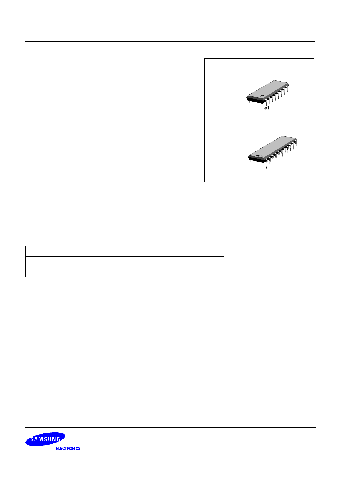
The S5G9801X01 is a 16-DIP type and is able to control 10 functions.
The S5G9803X01 is a 24-DIP type and is able to control 18 functions.
FEATURES
• Output for continuous pulse, toggle pulse and single pulse are
provided (Toggle pulse is available only for S5G9803X01)
• A single terminal type oscillator by means of RC is provided
• Containing custom code detection circuit for code check with
the transmitter (To prevent interferences with other models)
• Able to output in parallel method multiple keying signals sent
from transmitter.
The S5G9801X01 can output up to 5 functions, and the S5G9803X01 can output up to 6 functions in parallel
method.
16−DIP−300A
24−DIP−400
ORDERING INFORMATION
Device Package Operating Temperature
S5G9801X01-D0B0 16−DIP−300A
S5G9803X01-D0B0 24−DIP−400
− 20°C − +75°C
1
Page 2

S5G9801X01/S5G9803X01 INFRAED REMOCON RECEIVER
BLOCK DIAGRAM
V
GND
DD
16
1
OSC
REMIN
CODE1
CODE2
15
14
13
OSC
2
DATA
INPUT
SYSTEM
CODEINPUT
DIVIDER
DATABIT
COUNTER
COMPARATOR
CLOCK
GENERATOR
DATA
REGISTER
OUTPUT LATCH
& DRIVER
CP1
CP2
CP3
CP4
CP5
CP6
SP1
SP2
SP3
SP4
SP5
SP6
SP7
SP8
SP9
SP10
TP1
TP2
Figure 1.
2
Page 3

INFRAED REMOCON RECEIVER S5G9801X01/S5G9803X01
PIN CONFIGURATION
VSS
REMIN
CP1
CP2
CP3
CP4
CP5
SP5
1
2
3
4
S5G9801X01
5
6
7
8
16
15
14
13
12
11
10
9
VDD
OSC
CODE2
CODE3
SP1
SP2
SP3
SP4
VSS
REMIN
CP1
CP2
CP3
CP4
TP5
TP6
TP2
TP1
SP10
SP9
1
2
3
4
5
6
S5G9803X01
7
8
9
10
11
12
24
23
22
21
20
19
18
17
16
15
14
13
VDD
OSC
CODE1
CODE2
SP1
SP2
SP3
SP4
SP5
SP6
SP7
SP8
Figure 2.
3
Page 4

S5G9801X01/S5G9803X01 INFRAED REMOCON RECEIVER
PIN DESCRIPTION
Pin No
Symbol
S5G9801 S5G9803
Input
Output
1 1 GND Ground −
2 2 REMIN
3 − 7 − CP1 − SP5
− 3 − 8 CP1 − CP6
− 9 − 10 TP1, TP2
8 ~ 12 − SP1 − SP5
− 11 − 20 SP1 − SP10
Receiving Signal
Input
Continuous Signal
output
Toggle Signal
Output
Single Signal Output
Instruction signal input with the carrier signal
eliminated.
As long as receiving is input, this output is held at “H”
level. After releasing a key, output is held at “H” level
for about 160 msec.
When receiving signal is input, output is toggled.
When receiving signal is input, output is held at “H”
level only for about 107 msec.
A code set at this terminal is compared with tran-
13, 14 21, 22 CODE Code Input
smitter code and if they agree with each other, input is
accepted (built-in pull-up resistor).
15 33 OSC Timing Oscillation
A capacitor and a resistor are connected in parallel
method between this terminal and VSS.
16 24 VDD Power Supply −
Description
ABSOLUTE MAXIMUM RATINGS (TA = 25×C)
Characteristic Symbol Value Unit
Supply Voltage V
Input/Output Voltage VIN V
Power Dissipation P
Operating Temperature T
Storage Temperature T
DD
OUT
D
OPR
STG
0 − 6 V
VSS −0.3 − VDD + 0.3 V
200 mW
−20 − 75 °C
−55 − 125 °C
4
Page 5

INFRAED REMOCON RECEIVER S5G9801X01/S5G9803X01
ELECTRICAL CHARACTERISTICS
(Ta = 25 ×C, VDD = 5 V, unless otherwise specified)
Characteristic Symbol Test Conditions Min. Typ. Max. Unit
Operating Voltage V
Operating Current I
Frequency Deviation f
DD
DD
OSC
Ta = −25°C ~ 75°C 4.5 − 5.5 V
Output Without Load − − 1.0 mA
Ta = −25°C − 75°C
VDD = 4.5V − 5.5V
27 38 57 kHz
Frequency Stability
∆V
∆T
Output “H” Level I
Current “L” Level I
Input Current “H” Level I
Pull-up Resistor R
Input Circuit Threshold
Voltage
V
V
Hysteresis Width VH
Standard osc Frequency S
FOSC
FOXC
FOSC
OH
OL
IH
UP
IH
IL
2S
Ta = −25°C
VDD = 4.5V − 5.5V
−5 − 5 %
Ta = −30°C − 75°C −5 − 5 %
All Output, VOH = 4V − −2.0 −1.0 mA
All Output, VOL = 1V 1.0 2.5 − mA
Code Terminal, VIH = 5.0V −1.0 − 1.0 uA
REMAIN Terminal 10 20 40 kΩ
REMAIN Terminal 3.5 − − V
REMAIN Terminal − − 1.5 V
− − 1.0 − V
− − 38 − kHz
5
Page 6

S5G9801X01/S5G9803X01 INFRAED REMOCON RECEIVER
OPERATING PRINCIPLES
1. POR (Power On Reset) CIRCUIT
To initialize the internal state at time of power ON, it is necessary to perform the initialization.
The initialization is carried out when a capacitor is connected to the code bit terminal.
R
UP
CODE1 CODE2
R
UP
Figure 3.
In the case of S5G9803, connect a capacitor to CODE2 and CODE3.
2. OSCILLATION CIRCUIT
The RC oscillation circuit is normally operated at 38kHz oscillation frequency.
(The RC is connected between OSC terminal and VSS.)
Initialize
RUP = 20kΩ
C = 0.001µF − 0.022µF
FOSC
CSC
SCHMITT
R = 39kΩ ± 5%
C
R
C = 1000pF ± 5%
Figure 4.
Oscillation frequency is about 38kHz ± 5kHz at R = 38kW and C = 1000pF.
6
Page 7

INFRAED REMOCON RECEIVER S5G9801X01/S5G9803X01
3. RECEIVING SIGNAL INPUT CIRCUIT
Signal received by the light receiving element is sent through the Pre-Amp to the detector, when a 38 kHz carrier
wave is eliminated and the signal enters a REMIN PIN of the receiving signal input circuit. The receiving signal
input circuit (REMIN) has a built-in Schmitt trigger for shaping receiving signal waveforms to eliminate rounding.
AMP DET REMIN
PH302B
Figure 5.
4. RECEIVING SIGNAL CHECK
The receiving signal check is to check the 2-cycle transmitting signal sent from the transmitter to check whether it is
a normal signal or not.
12 Bits
First Data
12 Bits
Second Data
Figure 6.
The first data is stored in the 12-bit data register. Then, when the second data is entered, the previous data is
pushed out from the data register one by one.
The pushed out data and incoming data are checked to see if they are same.
If any errors are caused during the 12-bit receiving data check, the system is reset at that time. And when all receiving data are same, output is raised from L level to H level.
The status of receiving data, register clock and check pulse are shown below.
Register clock is provided in the data center by taking frequency margins of the transmitter and the receiver into
consideration.
7
Page 8

S5G9801X01/S5G9803X01 INFRAED REMOCON RECEIVER
DATA ‘1’
0.42ms 0.84ms
Receiving Data
Register Clock
(REGCK)
Check Pulse
(CHP)
READER
DATA ‘0’
READER
Figure 7.
5. CODE BIT COMPARISON
In order to prevent interference with other machines and apparatuses, C1, C2 and C3 code bits are provided for
checking whether or not the transmitter codes agree to the receiver codes.
Only when both codes agree, the internal latch pulse is generated to latch receiving data, and output is raised from
“L” level to “H” level.
If both codes do not agree, latch pulse is not generated and output remains at “L” level.
Code bits used differ depending on receiver as shown below:
CODE BIT
C1 C2
C3 C2
0 1
1 0
1 1
S5G9801X01C2, ⋅⋅⋅⋅⋅⋅ C3 is used.
S5G9803X01C1, ⋅⋅⋅⋅⋅⋅ C2 is used.
* CODE BIT “0”, “0” cannot be used.
8
Page 9

INFRAED REMOCON RECEIVER S5G9801X01/S5G9803X01
6. EXPLANATION OF OUTPUT PULSE SP, CP, TP
1) SP1 - SP10 (Single Pulse)
When a single key is depressed, after checking the 12-bit receiving data, if the data agree, a single pulse is output.
The output is raised from “L” level to “H” level and returned again to “L” level after about 107 msec.
KEY ON
Single Signal
Latch Pulse
Single Output
12Bits
12Bits
About 107 msec
Figure 8.
2) CP1 - CP6 (Continuous Pulse)
Continuous pulse is output by the first latch pulse after key ON. Output is kept at “H” level as a long as a continuous
signal is input.
When the key is released and continuous signal is stopped about 160 msec later, output is reversed to “L” level by
the last latch pulse.
Further, CP1 - CP6 are able to output simultaneously in parallel method, maximum sextet outputs at “H” level by
continuous signals sent from the transmitter.
These outputs are optimum as outputs of REC-PLAY, REC-PAUSE and CUE/REVIEW of a tape deck.
KEY ON
Continuous
Signal
Latch Pulse
12 12
Continuous
Output
Figure 9.
3) TP1, TP2 (Toggle Pulse)
When toggle signal is received, toggle pulse output is reversed.
This toggle pulse is used for power ON, OFF, MUTE, etc.
KEY ON
Toggle signal
Latch Pulse
Toggle Output
12 12
Figure 10.
160msc
9
Page 10

S5G9801X01/S5G9803X01 INFRAED REMOCON RECEIVER
7. CODE TABLE
C1 - C3 code bits are available in addition to the data bits shown below for optional code selection. S5G9803X01
is able to use all keys, but S5G9801X01 can use KEY1 - 5 and KEY 7 - A only for 10 commands.
Key Data Bit Key Data Bit
No. CT S1 S2 D1 D2 D3 D4 D5 D6 No. CT S1 S2 D1 D2 D3 D4 D5 D6
1 1 0 0 1 0 0 0 0 0 CONT, CP1 10 0 1 0 0 0 0 1 0 0 SING, SP4
2 1 0 0 0 1 0 0 0 0 CONT, CP2 A 0 1 0 0 0 0 0 1 0 SING, SP5
3 1 0 0 0 0 1 0 0 0 CONT, CP3 B 0 1 0 0 0 0 0 0 1 SING, SP6
4 1 0 0 0 0 0 1 0 0 CONT, CP4 C 0 0 1 1 0 0 0 0 0 SING, SP7
5 1 0 0 0 0 0 0 1 0 CONT, CP5 D 0 0 1 0 1 0 0 0 0 SING, SP8
6 1 0 0 0 0 0 0 0 1 CONT, CP6 E 0 0 1 0 0 1 0 0 0 SING, SP9
7 0 1 0 1 0 0 0 0 0 SING, SP1 F 0 0 1 0 0 0 1 0 0 SING, SP10
8 0 1 0 0 1 0 0 0 0 SING, SP2 G 0 0 1 0 0 0 0 1 0 TOGG, TP1
9 0 1 0 0 0 1 0 0 0 SING, SP3 H 0 0 1 0 0 0 0 0 1 TOGG, TP2
CONT : Continuous, SING : Single, TOGG : Toggle
NOTE: S5G9802X01 has 18 function keys, and total 75 commands can be transmitted: 63 commands by the continuous keys
of multiple keying is possible and 12 commands by the single-shot keys.
10
Page 11

INFRAED REMOCON RECEIVER S5G9801X01/S5G9803X01
EXAMPLE OF APPLICATION CIRCUIT
1. COMBINATION OF S5G9802X01/S5G9801X01 CODE BITS
(EXAMPLE 1) In the Case when CODE C2 = 0 and C3 = 1
(TABLE 1)
S5G9802X01 S5G9801X0
CCI
1
C1 C2 C3 C2 C3
1 0 1 0 1
1 1 0 1 0
1 1 1 1 1
V
DD
ST3 ST2 ST1 K6
(C3) (C2) (C1)
S5G9802
KS9802
(CODE C1 = 1,
C2 = 0, C3 =1)
(CODE C1 =1, C2 =1)
V
DD
CODE1 CODE1 SP1
OSC
Figure 11.
The combination of code bits of S5G9802X01 and S5G9801X01 is shown in Table 1.
To make the code bit to 1 on S5G9802X01, connect diodes to the CCI terminal from ST1 - ST3 terminals. To set
Code Bit at 0, open the circuit.
S5G9801X01 has CODE2 and CODE3 code terminals. Code bit of C1 has been pulled up in IC and C1 is always
kept at 1 status.
Therefore, on transmitter S5G9802X01, it is necessary to keep C1 code bit at 1.
11
Page 12

S5G9801X01/S5G9803X01 INFRAED REMOCON RECEIVER
2. COMBINATION OF S5G9802/S5G9803 CODE BITS
(TABLE 2)
(EXAMPLE 2) In case CODE C1 = 1 and C2 = 1
S5G9802X01 S5G9803X01
C1 C2 C3 C2 C3
0 1 1 0 1
CCI
ST3 ST2 ST1 K6
(C3) (C2) (C1)
S5G9802X01
KS9802
(CODE C1 = 1,
C2 = 1, C3 =1)
1 0 1 1 0
1 1 1 1 1
V
DD
V
DD
CODE1 CODE1
OSC
(CODE C1 =1, C2 =1)
Figure 12.
The combination of code bits of S5G9802X01 and S5G9803X01 is shown in Table 2.
S5G9803X01 has CODE1 and CODE2 code terminals. Code bit of C3 has been pulled up in IC and C3 is always
kept at 1 status.
Therefore, on transmitter S5G9802X01 it is necessary to keep code bit C3 at 1.
To keep code bit C3 at 1, connect a diode to the Cci terminal from ST3 terminal.
3. If input voltage above VDD +0.3 V may be applied to the REMIN Input Terminal (2 PIN), connect about ten resistors in series to the REMIN Input Terminal. (This is to prevent latch-up).
RECEIVING SIGNAL
10k¥Ø
REMIN (2 PIN)
Figure 13.
12
Page 13

INFRAED REMOCON RECEIVER S5G9801X01/S5G9803X01
APPLICATION CIRCUITS
1. RECEIVING PART
S1A2184
2. S5G9801 CIRCUIT
PH302B
1
λ
10¥ìF
3 4
2
4.7Ω
+
+
3.3µF
1µF
-
-
5 6 7
330pF
200KΩ
8
22KΩ
5V
Figure 14.
CR
V
DD
+
+
16 15 14 13 12 11 10 9
VDDOSC CODE2 CODE3 SP1 SP2 SP3 SP4
1000pF
1000pF
S5G9801X01
V
REMIN
SS
1 2 3 4 5 6 7 8
CP1 CP2 CP3 CP4 CP5 CP5
CONTROL SIGNAL
KS9801
1KΩ
55KΩ
REMOUT
KSC945
REMIN
¥Ø
10k
input
Figure 15.
CONTROL SIGNAL
13
Page 14

S5G9801X01/S5G9803X01 INFRAED REMOCON RECEIVER
3. S5G9803 CIRCUIT
10¥ìF
CR
V
DD
+
+
24 23 22 21 20 19 18
VDDOSC CODE3 CODE1 SP1 SP2 SP3 SP4
V
REMIN
SS
1 2 3 4 5 6 7 8
REMIN
1000pF
1000pF
S5G9801X01
KS9801
CP1 CP2 CP3 CP4 CP5 CP5
¥Ø
10k
input
CONTROL SIGNAL
Figure 16.
CONTROL SIGNAL
17 16 15 14 13
SP5 SP6 SP7 SP8
CP5 CP5 CP5 CP5
9 10 11 12
14
Page 15

INFRAED REMOCON RECEIVER S5G9801X01/S5G9803X01
VARIANCE OF OSCILLATION FREQUENCY BY R AND C
1) Variance of Oscillation Frequency by R
55
50
45
VDD = 5 V
C = 1000 pF
FREQ.
(kHz)
40
35
30
25
30 34 38
2) Variance of Oscillation Frequency by C
55
50
45
FREQ.
(kHz)
40
35
30
R (kΩ)
4642
50 54
VDD = 5 V
R = 39 kΩ
25
30 34 38
4642
C (pF)
50 54
15
Page 16

S5G9801X01/S5G9803X01 INFRAED REMOCON RECEIVER
NOTES
16
 Loading...