

Page 1

OSD PROCESSOR FOR MONITOR S5D2508A01
ORDERING INFORMATION
OVERVIEW
The S5D2508A01 is used to display some characters or symbols on a screen of monitor. Basically, the operation is to control the internal memory on chip and generate the R,G,B signals
for some characters or symbols. The R,G,B signals are synchronized with the horizontal sync. Then the R,G,B signals are
mixed with the main video signal in the Video Amp IC.
The font data for characters or symbols are stored in the internal ROM. This stored data are accessed and controlled by the
control data from a micro controller. The control data are transmitted through the I2C bus. All timing control signals including
the system clock are synchronized with the horizontal sync.
Therefore there is a PLL circuitry on chip.
FEATURES
• 256 ROM fonts (Each font consists of 12 x 18
dots.)
• Full Screen Memory Architecture
• Wide range PLL available (15 kHz — 120 kHz)
• Programmable vertical height of character
S5D2508A01-D0B0 16-DIP-300 0°C — 70°C
16-DIP-300
Device Package Operating Temperature
• Programmable vertical and horizontal positioning
• Character color selection up to 16 different colors
• Programmable background color (Up to 16 colors)
• Character blinking, bordering and shadowing
• Color blinking
• Character scrolling
• Fade-in and fade-out
• Box drawing
• Character sizing up to four times
• 96 MHz pixel frequency from on-chip PLL
• IIC Protocol Data Transmission (Slave Address : BAH)
1
Page 2
S5D2508A01 OSD PROCESSOR FOR MONITOR
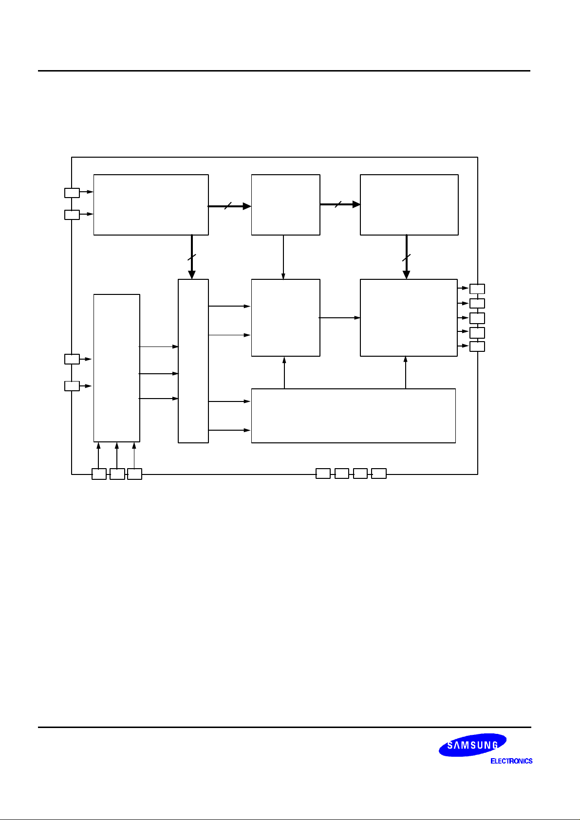
BLOCK DIAGRAM
SDA
SCL
HFLB
VFLB
ROM
Addr
9
Display
Control
Timing
Controller
Single Color ROM
(256 x 18x12)
Font
12
Data
Output
Stage
H/V/CLK
Control
15
14
13
12
11
INT
R_OU T
G_OUT
B_OUT
FBLK
Control
Data
Control
Control
Control
Control
RAM
Data
16
Frame
Row
Frame
Row
RAM
(480 x 16)
Font
Control
Display
Controller
H/V/CLK
Control
7
8
Data
Receiver
16
Control Register
CLK
6
OSD
_PLL
9
H-Pulse
V-Pulse
2 3 5 1 4 10 16
VCO_IN
VREF1
VREF
VSS_A
VDD_A
VSS_D
VDD_D
Figure 1. Functional Block Diagram
2
Page 3
OSD PROCESSOR FOR MONITOR S5D2508A01
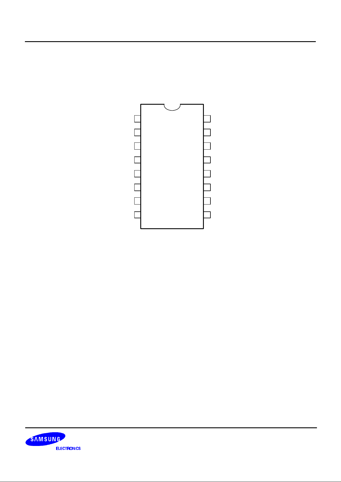
PIN CONFIGURATIONS
VSS-A
VCO-IN
VREF1
VDD-A
1
2
3
4
S5D2508A
5
VREF
6
HFLB
7
SDA
8
SCL
Figure 2. Pin Configurations
16
15
14
13
12
11
10
9
VDD_D
I
NT
R_OUT
G_OUT
B_OUT
FBLK
VSS_D
VFLB
3
Page 4
S5D2508A01 OSD PROCESSOR FOR MONITOR
PIN DESCRIPTIONS
Table 1. Pin Descriptions
Pin No. Signal Active I/O Description
1 VSS_A - - Ground (Analog Part)
2 VCO_IN - Input This voltage is generated at the external loop filter and
goes into the input stage of the VCO.
3 VREF1 - Input 1.26 V DC Voltage from the Bandgap Reference.
Connected to ground through a resistor to make internal
reference current (Typical 36 KΩ for 27µA)
4 VDD_A - - +5 V Supply Voltage for Analog Part
5 VREF - Input Bandgap Reference Voltage (Typical 1.26 V)
6 HFLB Low Input Horizontal Flyback Signal
7 SDA - In/Out
8 SCL - In/Out
9 VFLB Low Input Vertical Flyback Signal
10 VSS_D - - Ground for Digital Part
11 FBLK - Output Fast Blank Signal
12 B_OUT - Output Video Signal Output (B)
13 G_OUT - Output Video Signal Output (G)
14 R_OUT - Output Video Signal Output (R)
15 INT - Output Intensity Signal Output
16 VDD_D - - +5 V SUpply Voltage for Dogital Part
Serial Data (I2C)
Serial Clock (I2C)
4
Page 5
OSD PROCESSOR FOR MONITOR S5D2508A01
ABSOLUTE MAXIMUM RATINGS
Parameters Symbol Value Unit
Min. Typ. Max.
Maximum Supply Voltage VDD - - 7.0 V
Input Voltage V
Operating Temperature Range T
Storage Temperature Range T
Power Dissipation P
I
OPR
STG
D
- - 7.0 V
-20 - 70
-40 125
- - 1200 mW
NOTE: PKG Thermal Resistance : 64.2 °C/W
ELECTRICAL CHARACTERISTICS
DC Electrical Characteristics
(Ta = 25 °C, VDD = 5 V)
Table 2. DC Electrical Characteristics
Parameters (Conditions) Symbol Min. Typ. Max. Unit
Supply Voltage VDD 4.75 5.00 5.25 V
Supply Current
(No load on any output)
Input Voltage
I
V
V
DD
- - 25 mA
IH
IL
0.8VDD
-
-
-
- V
VSS + 0.4 V
°C
°C
Output Voltage
(lout = 1mA)
Input Leakage Current I
VCO Input Voltage V
V
V
VCO
OH
OL
IL
0.8VDD
- -
-10
-
- V
VSS + 0.4 V
-
10 µA
2.5 V
5
Page 6
S5D2508A01 OSD PROCESSOR FOR MONITOR
OPERATION TIMINGS
Table 3. Operation Timings
Parameters (Conditions) Symbol Min. Typ. Max. Unit
Output Signal - R/G/B_OUT, INT, FBLK (Ta = 25°C VDDA = VDD = 5 V , CLOAD = 30pF)
Rise Time t
Fall Time t
Input Signal - HFLB, VFLB
Horizontal Flyback Signal Frequency f
Vertical Flyback Signal Frequency f
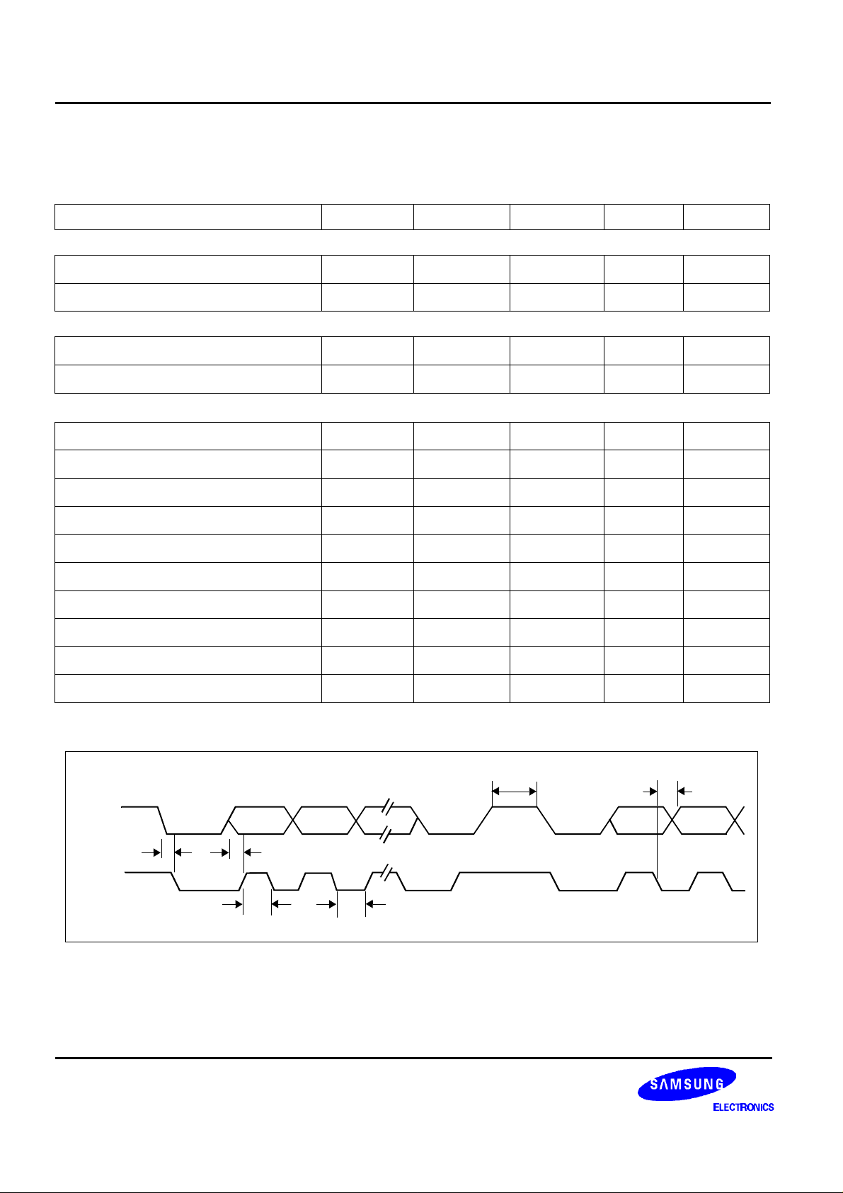
I2C Interface - SDA, SCL (Refer to Figure 3)
SCL Clock Frequency f
Hold Time for start condition t
Set Up Time for stop condition t
Low Duration of clock t
High Duration of clock t
Hold Time for data t
Set Up Time for data t
Time between 2 access t
Fall Time of SDA t
R
F
HFLB
VFLB
SCL
hs
sus
low
high
hd
sud
ss
fSDA
- - 6 nsec
- - 6 nsec
- - 120 kHz
- - 200 Hz
- - 300 kHz
500 - - ns
500 - - ns
400 - - ns
400 - - ns
0 - - ns
500 - - ns
500 - - ns
- - 20 ns
Rise Time of both SCL and SDA t
SDA
SCL
t
hs
t
t
high
sud
t
Figure 3. I2C Bus Timing Diagram
low
rSDA
- - - ns
t
t
ss
hd
6
Page 7
OSD PROCESSOR FOR MONITOR S5D2508A01
FUNCTIONAL DESCRIPTIONS
Data Transmission to the S5D2508A01
According to the I2C protocol, the S5D2508A01 receives the data from a micro controller. The SDA line and the
SCL line are shown in Figure 4. As shown in Figure 4, after the starting pulse, the slave address with R/W* bit and
an acknowledge are transmitted in sequence, an internal register address of the S5D2508A01 is followed. The first
8-bit byte is the upper 8bits of the register address. The lower 8bits of the register address are followed after the
second acknowledge. There is a data transmission format and are two address bit patterns in the S5D2508A01 as
following.
The slave address of the S5D2508A01 is BAH(in hexadecimal).
Data Transmission Format
Row Address -> Column Address -> Data Byte N -> Data Byte N+1 -> Data Byte N+2 -> ....
Address Bit Pattern for Display Registers Data
(a) Row Address Bit Pattern R3 - R0: Valid Data for Row Address
A15 A14 A13 A12 A11 A10 A9 A8
X X X X R3 R2 R1 R0
(b) Column Address Bit Pattern C4 - C0: Valid Data for Column Address
A7 A6 A5 A4 A3 A2 A1 A0
X X X C4 C3 C2 C1 C0
After addressing, data bytes are followed as the above data transmission format. The Figure 4 describes the data
transmission with the I2C bus protocol.
SCL
SDA
START IIC SLAVE ADDRESS ACK MSB ADDRESS ACK LSB ADDRESS ACK
SCL
SDA
DATA BYTE N(MSB DATA)
D1 D0D2D3D4D5D6D7
R/W
D1 D0D2D3D4D5D6D7
ACK DATA BYTE N(MSB DATA) ACK STOPACK DATA BYTE N(LSB DATA)
A5 A4 A3 A2 A1 A0A6A7A9 A8A10A11A12A13A14A15
D1 D0D2D3D4D5D6D7
...
...
Figure 4. SDA line and SCL line (Write Operation)
7
Page 8
S5D2508A01 OSD PROCESSOR FOR MONITOR
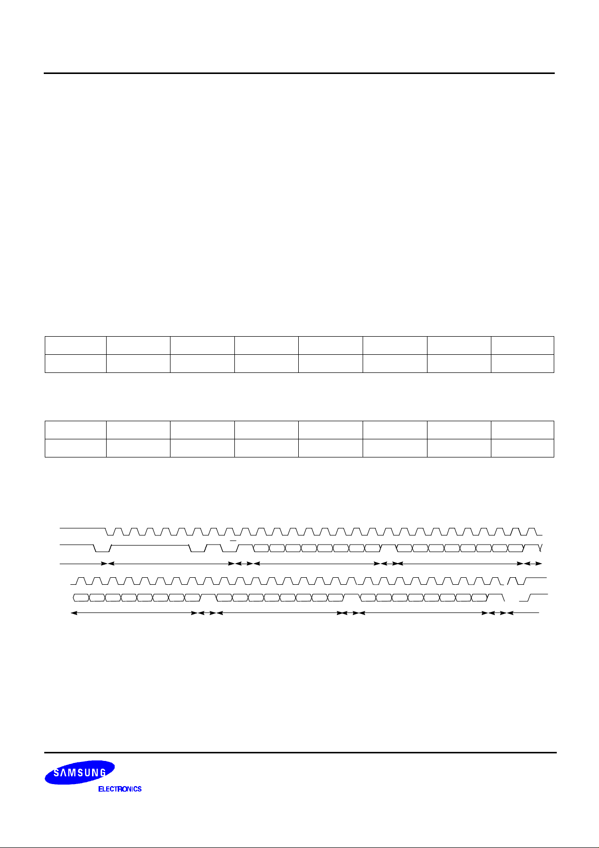
Memory Map
The display RAM is addressed with the row and column number in sequence. The display RAM consists of four
register groups: Character & Attribute Registers, Row Attribute Registers and Frame Control Registers-.
As the display area in a monitor screen is 30 columns by 15 rows, the related Character & Attribute Registers are
also 30 columns by 15 rows. Each register contains a character address and an attribute corresponding to display
location on a monitor screen. And one register is composed of 16 bits. The lower 8 bits select characters out of 256
ROM fonts. The upper 7 bits are assigned to give a character attribute to a selected font. Row Attribute Registers
occupy the 31th column of Display RAM and provide the row attribute of a blank mode, raster color, raster color
intensity, character color intensity, horizontal character size, vertical character size.
Frame Control Registers are located at the 16th row. The content of each register is described in Figure 5 and following register set.
00 01 02 27 28 29 30
Row 00
Row 01
Row 13
Row 14
Row 15
00 01 02
Frame Control Registers
Character & Attribute Registers
(30 x 15 Character Display)
Row Attribute
Registers
Figure 5. Memory Map of Display Registers
8
Page 9

OSD PROCESSOR FOR MONITOR S5D2508A01
ROM Fonts
S5D2508A01 is able to supply 256 single-color ROM fonts for describing an OSD icon. So a multi-language OSD
icon can be generated. The standard font $00 is reserved for blank data.
$0 0 $01 $02 $0 E $0F
$1 0 $11 $12 $1 E $1F
$2 0 $21 $22 $2 E $2F
$E 0 $E1 $E2 $E E $EF
$F0 $F1 $F2 $FE $FF
Figure 6. Array of ROM Fonts
9
Page 10
S5D2508A01 OSD PROCESSOR FOR MONITOR
Scroll
The scrolling function is to display or erase a character slowly from the top line to the bottom. The scrolling time is
controlled by 'ScrT' bit of the frame control registers. If 'ScrT' bit is high, then the time is 0.5 sec. Otherwise, 1 sec.
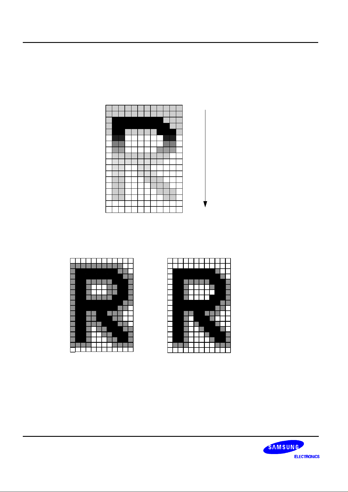
Character Bordering & Shadowing
Bordering Shadowing
10
Page 11

OSD PROCESSOR FOR MONITOR S5D2508A01
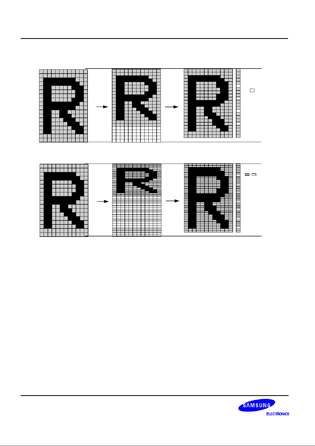
Character Height Control
Two examples of the height-controlled character are shown in the following figure. The height control is performed
by repeating some lines. The repeating line-number comes from the equation below.
[# of the repeating lines = 2 + N × M ] ,
where N = 1,2,3,... and M = round{14÷(CH[5:0]-18)}.
If the M value is less than or equal to 1, all the lines of the standard font are repeated once or more. This is
described as following.
(i) If CH[5:0] is greater than 32, and less than or equal to 46 (32 < CH[5:0] ≤ 46), then all lines are repeated once
or twice. The lines repeated twice are selected by the following equation.
[# of the repeating lines = 2 + N × M ] ,
where N = 1,2,3,... and M= round{14÷(CH[5:0]-32)}.
(ii) If CH[5:0] is greater than 46, and less than or equal to 60 (46 < CH[5:0] ≤ 60), then all lines are repeated twice
or three times. The lines repeated three times are selected by the following equation.
[# of the repeating lines = 2 + N × M ] ,
where N = 1,2,3,... and M= round{14÷(CH[5:0]-46)}.
iii) If CH[5:0] is greater than 60, and less than or equal to 64 (60 < CH[5:0] ≤ 64), then all lines are repeated three
or four times. The lines repeated four times are selected by the following equation.
[# of the repeating lines = 2 + N × M ] ,
where N = 1,2,3,... and M= round{14÷(CH[5:0]-60)}.
The repeating line-number is limited to 16.
11
Page 12
S5D2508A01 OSD PROCESSOR FOR MONITOR
1
2
3
4
5
6
Standard Font(12*18)
7
8
9
10
11
12
13
14
15
16
17
18
Standard font
in high vertical resolution
1
2
3
4
5
6
7
8
9
10
11
12
13
14
15
16
17
18
Height-controlled font
: added
line
: added
line
Standard Font(12*18)
Standard font
in more higher vertical resolution
Height-controlled font
12
Page 13
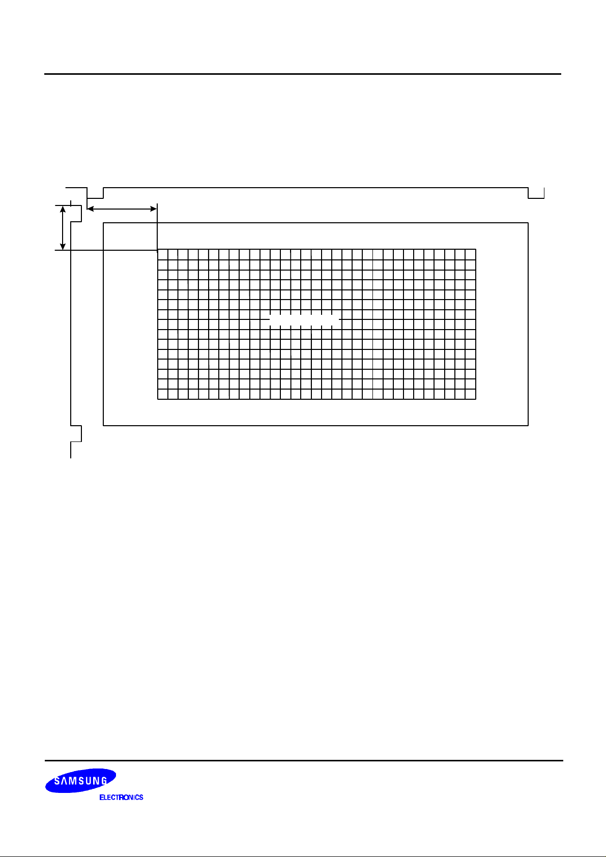
OSD PROCESSOR FOR MONITOR S5D2508A01
HFLB
FRAME CONTROL & TIMING
Figure 7 shows the composition of display frame with the OSD characters.
HP[7:0]
VP[7:0]
15 Rows(15 x 18 dots)
30 Columns(=30 x 12 dots)
OSD Characters
Background Screen
Figure 7. Frame Composition with the OSD Characters
User can determine the dot frequency by the equation of H freq. x the number of horizontal resolution.
And the number of horizontal resolution is determined by the bit9 - 8 (dot 1,dot 0) of the frame Control registers-1.
If dot 0 = “0”, dot 1 = “0”, then the dot frequency is calculated by the equation of H freq. × 320.
If the H freq. = 15 kHz, then the dot frequency is 15 kHz × 320 = 4.8 MHz.
If dot 0 = “1”, dot 1 = “1” and the horizontal frequency is 120 kHz, then the dot frequency is 120 kHz × 800 = 96
MHz. 96 MHz is the maximum clock frequency in this processor.
13
Page 14

S5D2508A01 OSD PROCESSOR FOR MONITOR
REGISTER DESCRIPTION
¡ß
Character & Attribute Register : Row00~14, Column00~29
F E D C B A 9 8 7 6 5 4 3 2 1 0
BINV BOX1 BOX0 B G R Blink - C7 C6 C5 C4 C 3 C2 C1 C0
Character Attribute Character Code 256 Fonts)
¡ß
Row Attribute Register : Row00~14, Column30
F E D C B A 9 8 7 6 5 4 3 2 1 0
- BREN I NTE CBli BOXE BORD SHA RB RG R R RINT CINT HZ 1 H Z0 VZ1 VZ0
Raster Color Intensity Character Size
¡ß
Frame Control Register 0 : Row15, Column00
F E D C B A 9 8 7 6 5 4 3 2 1 0
- F de FdeT VPOL HPOL - - - - Erase EN ScrI ScrT Bli1 Bli0 BliT
¡ß
Frame Control Register 1 : Row15, Column01
F E D C B A 9 8 7 6 5 4 3 2 1 0
CP1 CP0 F pll H F 2 HF1 H F0 dot1 dot0 D PLL FBLK CH 5 CH4 CH3 C H2 C H1 CH 0
PLL Control Character Height Control
¡ß
Frame Control Register 2 : Row15, Column02
F E D C B A 9 8 7 6 5 4 3 2 1 0
HP7 HP6 H P5 HP4 H P3 HP2 H P1 HP0 VP7 VP6 VP5 VP4 VP3 VP2 VP1 VP0
Horizontal Start Position Vertical Start Pos ition
14
Page 15

OSD PROCESSOR FOR MONITOR S5D2508A01
Table 4. Register Description
Registers Bits Description
Character & Attribute
Register (Row 00—14,
Column 00~29)
C7—C0
(Bit 7—0)
Blink/FINT
(Bit 9)
B,G,R
(Bit C—A)
BOX 1,
BOX0
(Bit E, D)
Character Code Address of 256 ROM Fonts.
Character Blinking/Font Intensity Enable.
If ‘INTE’ bit is low, this bit control blinking effect. The blinking period is
set by the 'BliT' bit and the duty is selected by the 'Bli0' and ' Bli1' bits.
If ‘INTE’ bit is high, this bit control the font intensity combined with
‘INTE’, ‘RINT’ and ‘CINT’ as following table.
INTE Blink/FINT RINT CINT Function
0 0 - - Normal
0 1 - - Blink
1 0 - - Normal(No Intensity)
1 1 0 1 Character Intensity
1 1 1 0 Raster Intensity
1 1 1 1 Character & Raster Intensity
Character color is determined by these bits. 8 colors can be selected
and the color intensity of a character is given by 'CINT' bit of Row
Attribute Regisers. So user can select up to 16 colors.
Character Box Drawing.
The combinations of this two bits generate four different box drawing
modes as following. The following example is the case that box
dawing is activated with the font 'A'
BOX0
BOX1
0
1
0 1
BOX OFF
A
AA
* Bit F—D(RB/RG/RR) is also used for raster color by setting the
'BOXE' bit low. if the 'BOXE' bit is low,Raster color of a font is
determined by this bits . Priority of raster color selected here is
higher than that of row attribute.
15
Page 16
KA2201 1.2W AUDIO POWER AMP
Table 4. Register Description (Continued)
Registers Bits Description
Row Attribute Register
(Row 00 ~ 14, Column 30)
BINV
(Bit F)
VZ1,VZ0
(Bit 1, 0)
HZ1,HZ0
(Bit 3, 2)
Box Inversion.
The box drawing activated by the bit E and D is changed to white
box from black and conversely.
Vertical Character Size Control. Vertical character size is determined
by the combinations of this two bits as following table.
VZ1 VZ0 Vertical Character Size
0 0 1X
0 1 2X
1 0 3X
1 1 4X
Horizontal Character Size Control. The horizontal character size is
determined by the combinations of this two bits as following table.
HZ1 HZ0 Horizontal Character Size
0 0 1X
0 1 2X
1 0 3X
1 1 4X
CINT
(Bit 4)
RINT
(Bit 5)
RB,RG,RR
(Bit 8—6)
SHA Character Shadowing. Set this bit to activate characters shadowing.
BORD Character Bordering. Set this bit to activate characters shadowing.
Character Color Intensity. If ‘INTE’ bit and this bit is set, the color
intensity of characters setting ‘FINT’ bit in the same row is high.
Raster Color Intensity. If ‘INTE’ bit and this bit is set, the color
intensity of rasters setting ‘FINT’ bit in the same row is high.
Raster Color is determined by these bits. 8 colors can be selected
and the color intensity of a character is given by ‘RINT’ bit of Row
Attribute Registers. So it can be selected up to 16 colors.
Page 17
OSD PROCESSOR FOR MONITOR S5D2508A01
Table 4. Register Description (Continued)
Registers Bits Description
BOXE
(Bit B)
BOX Enable. If this bit is set, Bit F-D in the Character & Attribute
Registers are used for the box-drawing function.
Otherwise,those are used for raster color of a font. Even though the
raster color attribute is given by Bit 8-6 in the row attribute registers,
the priority of Bit F-D in the character & attribute registers is higher.
CBli
(Bit C)
Color Blink Enable. If this bit is high, color blinking effect is activated.
The effect is to repeat color inversion between character and raster.
Color blinking time and the duty is controlled by Bil T, Bil 1 and Bli 0.
INTE
(Bit D)
Intensity Enable.
If this bit is set, the function of RINT and CINT bit are enabled and the
bit 9 of Character & Attribute Register control the font intensity effect.
Otherwise, all intensity functions are disabled and the bit 9 of Charac-
ter & Attribute Register control the blinking effect.
BREN
(Bit E)
Back Raster Blank Enable.
If this bit is high and the raster color is black, the raster is transparent
Bit F Reserved
17
Page 18

S5D2508A01 OSD PROCESSOR FOR MONITOR
Table 4. Register Description (Continued)
Registers Bits Description
Frame Control Register 0
(Row 15, Column 00)
Bli T
(Bit 0)
Bli 1,Bli 0
(Bit 2,1)
ScrT
(Bit 3)
Scrl
(Bit 4)
EN
(Bit 5)
Erase
(Bit 6)
Blink Time Control.
If this bit is high, the blink time is 0.5 sec. Otherwise, 1 sec.
Blinking Duty Control.
The blinking duty is controlled by the combination of this two bits as
following.
Bli 1 Bli 0 Blinking Duty
0 0 Blink Off
0 1 Duty 25%
1 0 Duty 50%
1 1 Duty 75%
Scroll Time Control.
If this bit is high, the scroll time is 0.5 sec. Otherwise, 1 sec.
Scroll Enable.
The scroll display is activated by setting this bit high.
OSD Enable.
If this bit is high, OSD is enable. Otherwise, disable.
RAM Erasing.
RAM data are erased by setting this bit.
Bit A — 7 Reserved.
HPOL
Polarity of Horizontal Fly Back Signal. Positive 1, Negative 0
(Bit B)
VPOL
Polarity of Vertical Fly Back Signal. Positive 1, Negative 0
(Bit C)
FdeT
(Bit D)
Fde
(Bit E)
Fade-in and fade-out Time Control.
If this bit is high, the time is 0.5 sec. Otherwise, 1 sec.
Fade-in and fade-out Enable.
The fade-in and fade-out effect is activated by setting this bit high.
Bit F Reserved.
18
Page 19
OSD PROCESSOR FOR MONITOR S5D2508A01
Table 4. Register Description (Continued)
Registers Bits Description
Frame Control Register 1
(Row 15, Column 01)
CH5—CH0
(Bit 5—0)
FBLK
(Bit 6)
DPLL
(Bit 7)
dot 1,dot 0
(Bit 9,8)
HF2—HF0
(Bit C—A)
Character Height Control. The vertical character size is determined
by the bit 'VZ1' and VZ0'. According to the value made by this six
bits, the character height is determined.
If the value is 32, the number of vertical pixel of character font is 32.
Eventually, the character height is expanded from 18 to 63.
The binary vlaue must be greater than 18.
It determines the configuration of FBLK output pin. When it is clear,
FBLK pin outputs high during displaying characters or rasters.
Otherwise,FBLK pin outputs high only during displaying characters.
It determines the PLL scheme. If this bit is low, then the PLL mode is
differential mode. Otherwise, single mode.
This two bits determine the number of dots per horizontal line.
dot 1 dot 0 No. of Dots
0 0 320 dots/line
0 1 480 dots/line
1 0 640 dots/line
1 1 800 dots/line
The horizontal frequency information is transferred by this three bits.
HF2 HF1 HF0 Hf Information
FPLL
(Bit D)
CP 1,CP 0
(Bit F,E)
0 0 0 15 KHz < Hf < 20 KHz
0 0 1 20 KHz ≤ Hf <35 KHz
0 1 0 35 KHz ≤ Hf < 50 KHz
0 1 1 50 KHz ≤ Hf < 65 KHz
1 0 0 65 KHz ≤ Hf <80 KHz
1 0 1 80 KHz ≤ Hf < 95 KHz
1 1 0 95 KHz ≤ Hf < 110 KHz
1 1 1 110 KHz ≤ Hf < 120 KHz
If this bit is high, the VCO block of OSD_PLL operates on full range
(4MHz - 96 MHz).
This bit controls charge pump output current.
CP 1 CP 0 Charge Pump Current
0 0 0.5mA
0 1 0.75mA
1 0 1.0mA
1 1 1.25mA
19
Page 20

S5D2508A01 OSD PROCESSOR FOR MONITOR
Table 4. Register Description (Continued)
Registers Bits Description
Frame Control Register 2
(Row 15, Column 02)
VP7—VP0
(Bit 7—0)
HP7—HP0
(Bit F—8)
Vertical Start Position Control.
It means the top margin height from the V-sync reference edge.
( = VP[7:0] × 4 )
Horizontal Start Position Control.
It means the horizontal display delay from the H-sync reference
edge to the 1'st pixel position of characters. ( = HP[7:0] × 6 )
20
Page 21

OSD PROCESSOR FOR MONITOR S5D2508A01
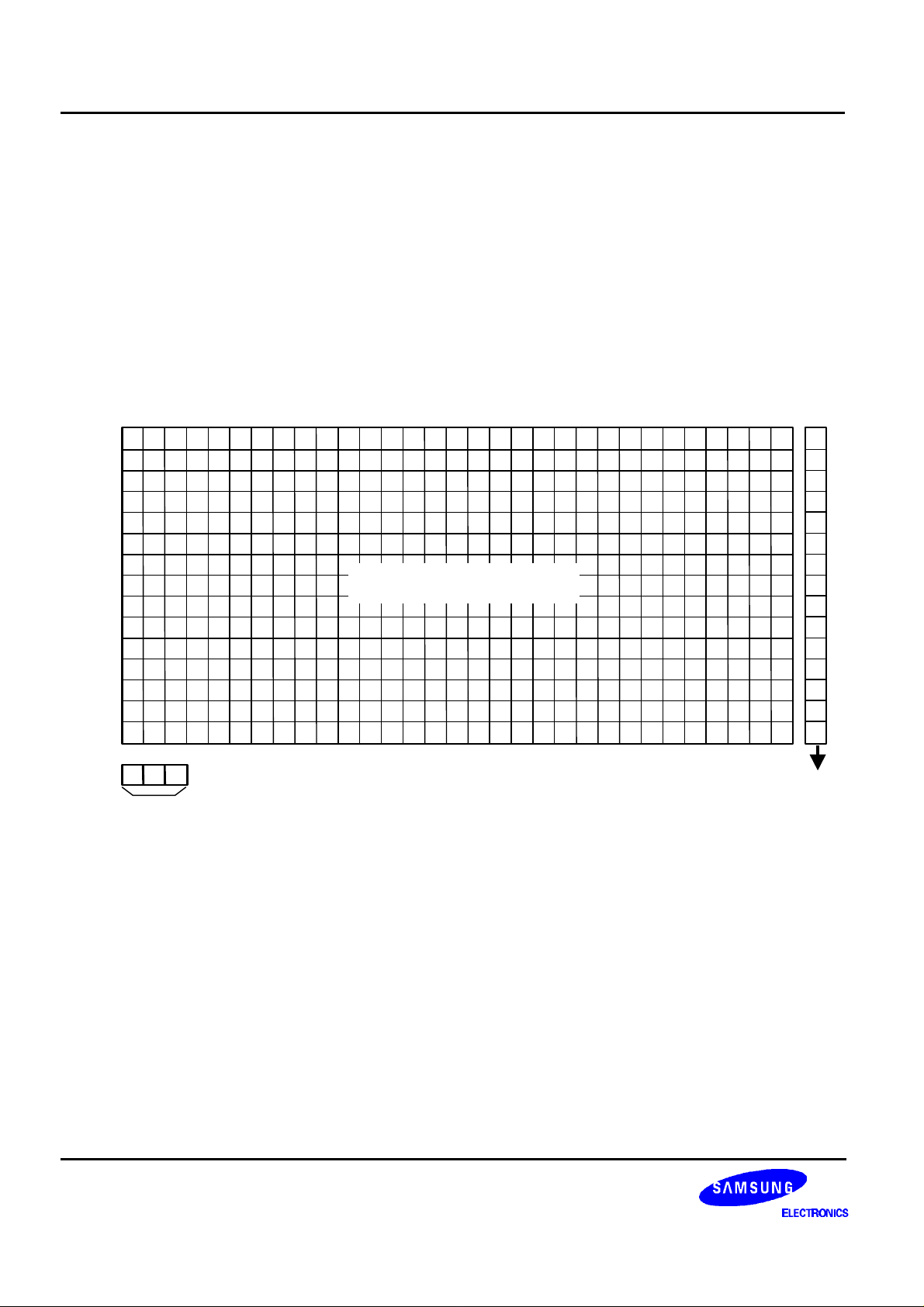
STANDARD ROM FONTS
21
Page 22

S5D2508A01 OSD PROCESSOR FOR MONITOR
22
Page 23
OSD PROCESSOR FOR MONITOR S5D2508A01
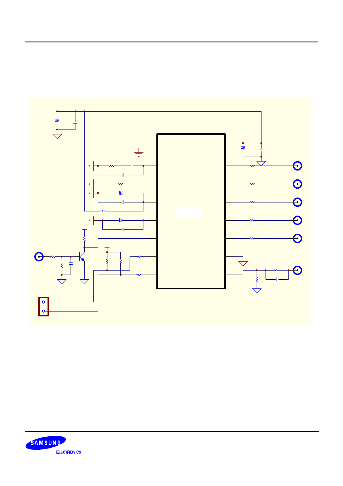
APPLICATION CIRCUIT
VCC=5V
+
100uF 104
+
1
VSS_A
VDD_D
16
100uF
104
HFLB
120
1
2
SDA
SCL
120
102
VCC
470
2N3904
Bead
1uH
VCC
5.6K
4.7K
101
36K
100uF
+
104
4.7uF
+
104
4.7K
392
2K
2K
2
3
4
5
6
7
8
VCO_IN
VREF1
VDD_A
VREF
HFLB
SDA
SCL
KS2508
S5D2508A
INT
R_OUT
G_OUT
B_OUT
FBLK
VSS_D
VFLB
15
14
13
12
11
10
9
400
400
400
400
400
120
6.2K
2.2nF
INT
R_OUT
G_OUT
B_OUT
FBLK
VFLB
23
Page 24

S5D2508A01 OSD PROCESSOR FOR MONITOR
NOTES
24
 Loading...