

Datasheet S48SS3R304NRFA, S48SS1R805NRFA, S48SS05002NRFA, S48SS05003NRFA, S48SS12001NRFA Datasheet (Delta Electronics)
...Page 1
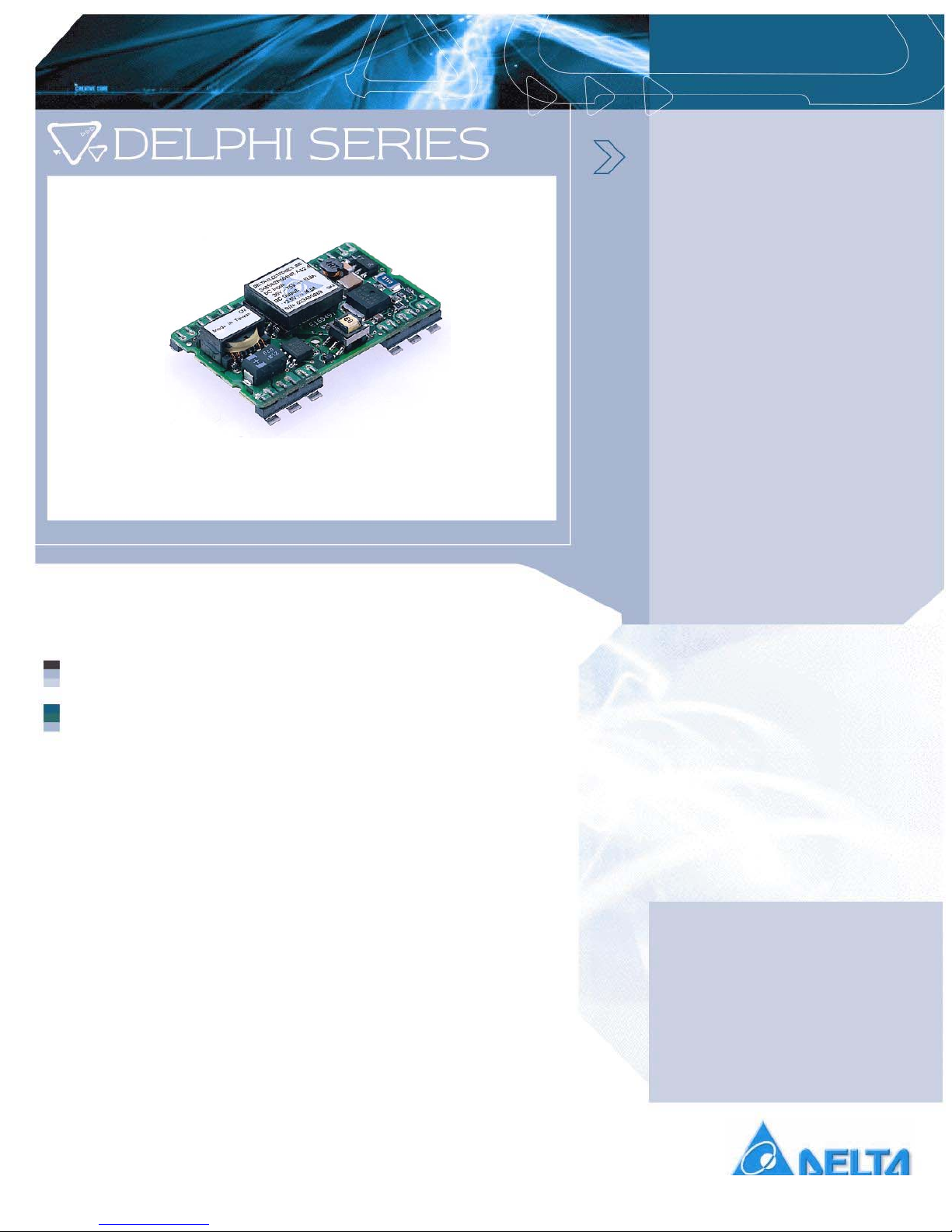
FEATURES
High efficiency: 86.5% @ 12V/1.25A
Standard footprint
Surface mountable
Industry standard pin out
Low profile: 0.48”
Fixed frequency operation
Input UVLO, Output OCP, OVP
No minimum load required
2:1 input voltage range
ISO 9001, TL 9000, ISO 14001, QS
9000, OHSAS 18001 certified
manufacturing facility
UL/cUL 60950 (US & Canada)
Recognized, and TUV (EN60950)
Certified
CE mark meets 73/23/EEC and
93/68/EEC directives
Delphi Series S48SS, 15W Family
DC/DC Power Module: 48V in, 12V/1.25A out
The Delphi Series S48SS, surface mountable, 48V input, single output,
isolated DC/DC converter, is the latest offering from a world leader in
power system and technology and manufacturing- Delta Electronics,
Inc. This product family provides up to 15 watts of power or up to 4.5A
of output current (for 3.3V and below) in an industry standard footprint.
With creative design technology and optimization of component
placement, the Delphi Series Small Power converters possess
outstanding electrical and thermal performance, as well as extremely
high reliability under highly stressful operating conditions. All models
are protected from abnormal input/output voltage and current
conditions. An encapsulated version is available for the most robust
performance in harsh environments.
Applications
Telecom/DataCom
Wireless Networks
Optical Network Equipment
Server and Data Storage
Industrial/Test Equipment
DATASHEET
DS_S48SS12001_06082006
DS_S48SS12001_06082006
1
Delta Electronics, Inc.
Page 2
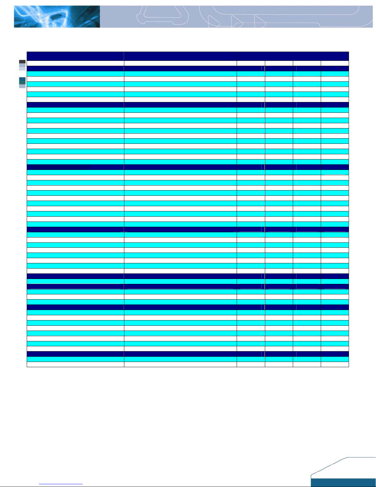
TECHNICAL SPECIFICATIONS
A
pp
(TA=25°C, airflow rate=300 LFM, Vin=48Vdc, nominal Vout unless otherwise noted.)
PARAMETER NOTES and CONDITIONS S48SS12001NRFA
Min. Typ. Max. Units
ABSOLUTE MAXIMUM RATINGS
Input Voltage
Continuous 80 Vdc
Transient (100ms) 100ms 100 Vdc
Operating Temperature Refer to Figure 12 for the measuring point -40 100 °C
Storage Temperature -55 125 °C
Input/Output Isolation Voltage 1 minute 1500 Vdc
INPUT CHARACTERISTICS
Operating Input Voltage 36 48 75 V
Input Under-Voltage Lockout
Turn-On Voltage Threshold 33.8 34.5 35.8 V
Turn-Off Voltage Threshold 32.0 33.5 34.5 V
Lockout Hysteresis Voltage 0.5 1.5 2.5 V
Maximum Input Current 100% Load, 36Vin 0.6 A
No-Load Input Current 25 mA
Off Converter Input Current 1
Inrush Current(I2t) 0.01 A2s
Input Reflected-Ripple Current P-P thru 12µH inductor, 5Hz to 20MHz 5 mA
Input Voltage Ripple Rejection 120 Hz 55 dB
OUTPUT CHARACTERISTICS
Output Voltage Set Point Vin=48V, Io=50% Io, max, Tc=25℃ 11.76 12.00 12.24
Output Voltage Regulation
Over Load Io=Io,min to Io,max ±12 ±60 mV
Over Line Vin=36V to 75V ±12 ±36 mV
Over Temperature Tc=-40℃ to 100℃ 100 300
Total Output Voltage Range Over sample load, line and temperature TBD TBD V
Output Voltage Ripple and Noise 5Hz to 20MHz bandwidth
Peak-to-Peak Full Load, 1µF ceramic, 10µF tantalum 50 100 mV
RMS Full Load, 1µF ceramic, 10µF tantalum 15
Operating Output Current Range 0 1.25 A
Output DC Current-Limit Inception Output Voltage 10% Low 1.5 2 2.5 A
DYNAMIC CHARACTERISTICS
Output Voltage Current Transient 48V, 10µF Tan & 1µF Ceramic load cap, 0.1A/µs
Positive Step Change in Output Current 50% Io, max to 75% Io, max 100 240 mV
Negative Step Change in Output Current 75% Io, max to 50% Io, max 100 240 mV
Setting Time to 1% of Final Value 600 µs
Turn-On Transient
Start-Up Time, From On/Off Control 35 50 ms
Start-Up Time, From Input 35 50
Maximum Output Capacitance Full load; 5% overshoot of Vout at startup 47 µF
EFFICIENCY
100% Load
ISOLATION CHARACTERISTICS
Isolation Voltage 1500 V
Isolation Resistance 100 MΩ
Isolation Capacitance 500 pF
FEATURE CHARACTERISTICS
Switching Frequency 260 kHz
ON/OFF Control, (Logic Low-Module ON)
Logic Low Von/off at Ion/off=1.0mA 0 0.8 V
Logic High Von/off at Ion/off=0.0 µA 15 V
ON/OFF Current Ion/off at Von/off=0.0V 1 mA
Leakage Current Logic High, Von/off=15V 50 µA
Output Voltage Trim Range
Output Over-Voltage Protection Over full temp range; % of nominal Vout 115 125 140 %
GENERAL SPECIFICATIONS
Calculated MTBF Io=80% of Io, max; Tc=40°C 3 M hours
Weight 12.5 grams
84 86.5 %
Across Trim Pin & +Vo or -Vo, Pout≦max rated power -10 +10 %
25
m
V
m/℃
mV
ms
DS_s48SS12001_06082006
2
Page 3
ELECTRICAL CHARACTERISTICS CURVES
)
90
36Vin 48Vi n 75Vi n
85
EFF ICIEN CY (%)
80
POWE R D ISSIPATIO N ( W
4.0
3.5
3.0
2.5
36Vin
48Vin 75Vin
75
70
65
60
0.25 0.5 0.75 1 1.25
OUTPUT CURRENT (A)
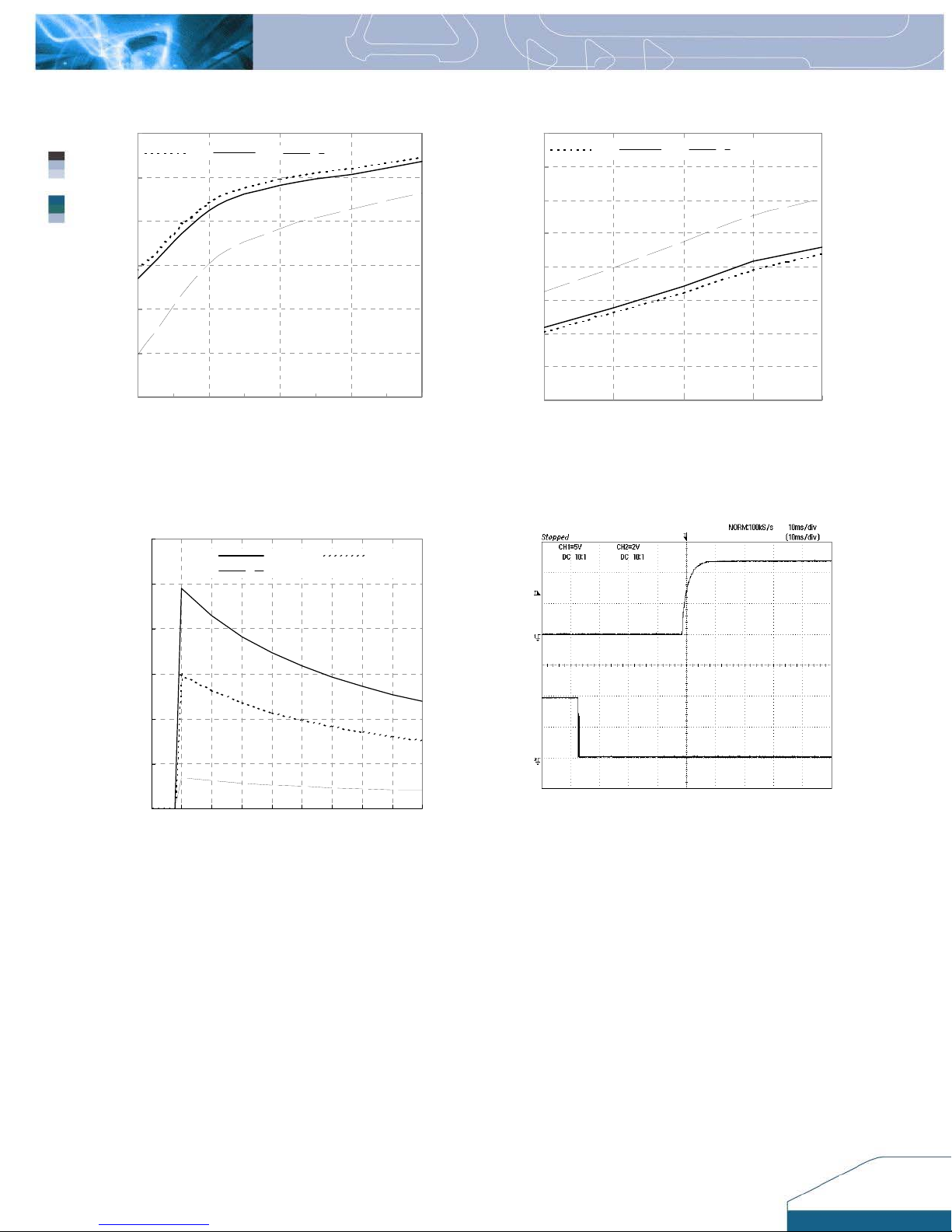
Figure 1: Efficiency vs. load current for minimum, nominal, and
maximum input voltage at 25
°C.
0.6
0.5
INPUT CURRENT (A)
0.4
0.3
Io=1.25A Io=0.75A
Io=0.125A
2.0
1.5
1.0
0.5
0.0
0.25 0.5 0.75 1 1.25
OUTPUT CURRENT (A)
Figure 2: Power dissipation vs. load current for minimum,
nominal, and maximum input voltage at 25
°C.
0.2
0.1
0.0
30 35 40 45 50 55 60 65 70 75
INPU T VOLTAGE (V)
Figure 3: Typical input characteristics at room temperature. Figure 4: Turn-on transient at full rated load current (resistive
load) (10 ms/div). Top Trace: Vout (5V/div); Bottom Trace:
ON/OFF Control (2V/div).
DS_s48SS12001_06082006
3
Page 4
ELECTRICAL CHARACTERISTICS CURVES
p
)
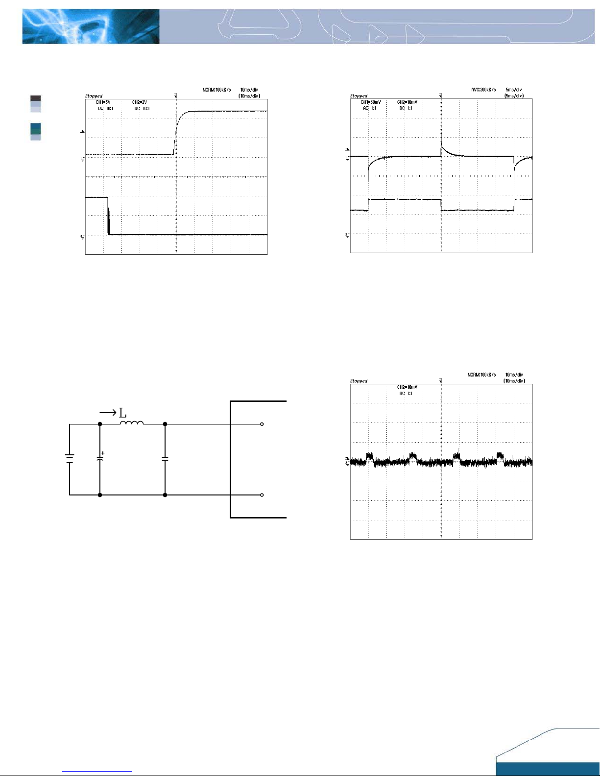
Figure5: Turn-on transient at zero load current (10 ms/div). Top
Trace: Vout (5V/div); Bottom Trace: ON/OFF Control (2V/div).
i
s
TEST
12uH
Cs:68uF/100V 68uF/100V
ESR< 0.3 ESR< 0.3
Ω
20﹫100KHz℃20 ℃100KHz﹫
Ω
Vi(+)
Vi(-)
Figure 6: Output voltage response to step-change in load
current (50%-75%-50% of Io, max; di/dt = 0.1A/µs). Load
cap: 10µF, 100 m
ceramic capacitor. Top Trace: Vout (50mV/div), Bottom
Trace: Iout (0.5A/div).
Ω
ESR tantalum capacitor and 1µF
Figure 7: Test set-up diagram showing measurement points for
Input Reflected Ripple Current (Figure 8).
Note: Measured input reflected-rip
source Inductance (L
battery impedance.
of 12 µH. Capacitor Cs offset possible
TEST
le current with a simulated
DS_s48SS12001_06082006
Figure 8: Input Reflected Ripple Current, i
output current and nominal input voltage with 12µH source
impedance and 68µF electrolytic capacitor (2 mA/div)
, at full rated
s
4
Page 5
ELECTRICAL CHARACTERISTICS CURVES
E
StripCopper
Vo(+)
SCOPE RESISTIV
10u
Vo(-)
1u
LOAD
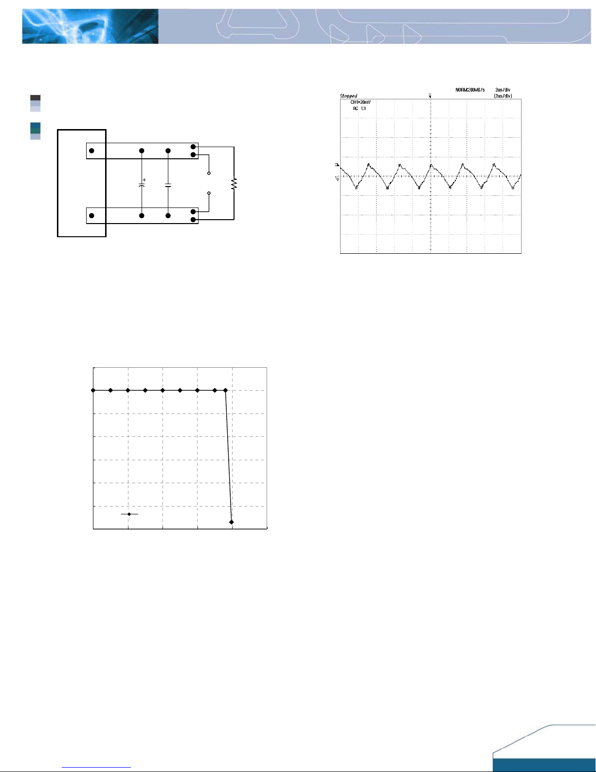
Figure 9: Output voltage noise and ripple measurement test
setup. Scope measurement should be made using a BNC
cable (length shorter than 20 inches). Position the load
between 51 mm to 76 mm (2 inches to 3 inches) from the
module.
14.0
12.0
10.0
OUT PUT VOLTAG E (V)
8.0
6.0
4.0
2.0
0.0
0.0 0.5 1.0 1.5 2.0 2.5
Vin= 48V
LOAD CURRENT (A)
Figure 11: Output voltage vs. load current showing typical
current limit curves and converter shutdown points.
Figure 10: Output voltage ripple at nominal input voltage and
rated load current (20 mV/div). Load capacitance: 1µF ceramic
capacitor and 10µF tantalum capacitor. Bandwidth: 20 MHz.
DS_s48SS12001_06082006
5
Page 6
THERMAL CURVES:
Top View
S48SS12001NR A Output Current vs. Ambient Temperature and Air Velocity @Vin < 60V
Output Current(A)
1.3
1.2
1.1
1.0
0.9
0.8
0.7
0.6
0.5
0.4
0.3
0.2
0.1
0.0
75 80 85 90 95 100 105
Natural
Convection
100LFM
200LFM
300LFM
600LFM
500LFM
400LFM
Ambient Temperature (℃)
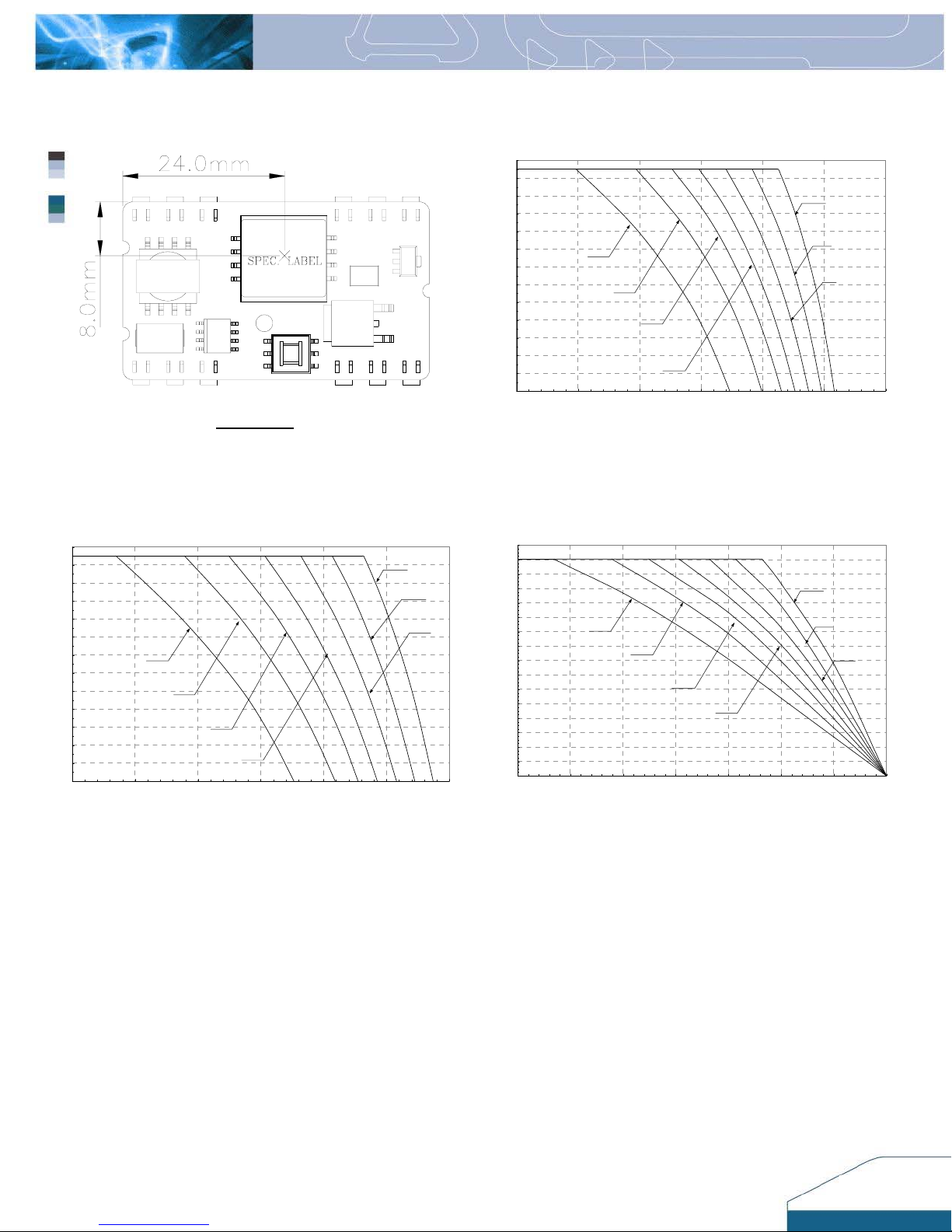
Figure 12: Case temperature measurement location. Pin locations are
for reference only.
Figure 13: Output current vs. ambient temperature and air velocity (Vin
<60V)
S48SS12001NR A Output Current vs. Ambient Temperature and Air Velocity @Vin = 75V
Output Current(A)
1.3
1.2
1.1
1.0
0.9
0.8
0.7
0.6
0.5
0.4
0.3
0.2
0.1
0.0
70 75 80 85 90 95 100
Natural
Convection
100LFM
200LFM
300LFM
Figure 14: Output current vs. ambient temperature and air velocity
(Vin=75V)
600LFM
500LFM
400LFM
Ambient Temperature (℃)
Figure 15: Power dissipation vs. ambient temperature and air
velocity.
S48SS12001NR A Power Dissipation vs. Ambient Temperature and Air Velocity
Power Dissipation (Watts)
3.2
3.0
2.8
2.6
2.4
2.2
2.0
1.8
1.6
1.4
1.2
1.0
0.8
0.6
0.4
0.2
0.0
70 75 80 85 90 95 100 105
Natural
Convection
100LFM
200LFM
300LFM
600LFM
500LFM
400LFM
Ambient Temperature (℃)
DS_s48SS12001_06082006
6
Page 7

DESIGN CONSIDERATION
Input Source Impedance
The impedance of the input source connecting to the
DC/DC power modules will interact with the modules
and affect the stability. A low ac-impedance input
source is recommended. If the source inductance is
more than a few µH, we advise adding a 10 to 100 µF
electrolytic capacitor (ESR < 0.7 Ω at 100 kHz)
mounted close to the input of the module to improve the
stability.
Layout and EMC Considerations
Delta’s DC/DC power modules are designed to operate
in a wide variety of systems and applications. For
design assistance with EMC compliance and related
PWB layout issues, please contact Delta’s technical
support team. An external input filter module is
available for easier EMC compliance design.
Application notes to assist designers in addressing
these issues are pending release.
Safety Considerations
The power module must be installed in compliance with
the spacing and separation requirements of the enduser’s safety agency standard if the system in which the
power module is to be used must meet safety agency
requirements.
When the input source is 60Vdc or below, the power
module meets SELV (safety extra-low voltage)
requirements. If the input source is a hazardous voltage
which is greater than 60 Vdc and less than or equal to
75 Vdc, for the module’s output to meet SELV
requirements, all of the following must be met:
The input source must be insulated from any
hazardous voltages, including the ac mains, with
reinforced insulation.
One Vi pin and one Vo pin are grounded, or all the
input and output pins are kept floating.
The input terminals of the module are not operator
accessible.
A SELV reliability test is conducted on the system
where the module is used to ensure that under a
single fault, hazardous voltage does not appear at
the module’s output.
Do not ground one of the input pins without grounding
one of the output pins. This connection may allow a nonSELV voltage to appear between the output pin and
ground.
This power module is not internally fused. To achieve
optimum safety and system protection, an input line
fuse is highly recommended. The safety agencies
require a normal-blow fuse with 1A maximum rating to
be installed in the ungrounded lead. A lower rated fuse
can be used based on the maximum inrush transient
energy and maximum input current.
Soldering and Cleaning Considerations
Post solder cleaning is usually the final board assembly
process before the board or system undergoes electrical
testing. Inadequate cleaning and/or drying may lower
the reliability of a power module and severely affect the
finished circuit board assembly test. Adequate cleaning
and/or drying is especially important for un-encapsulated
and/or open frame type power modules. For assistance
on appropriate soldering and cleaning procedures,
please contact Delta’s technical support team.
DS_s48SS12001_06082006
7
Page 8
FEATURES DESCRIPTIONS
Over-Current Protection
The modules include an internal output over-current
protection circuit, which will endure current limiting for
an unlimited duration during output overload. If the
output current exceeds the OCP set point, the modules
will automatically shut down (hiccup mode).
The modules will try to restart after shutdown. If the
overload condition still exists, the module will shut down
again. This restart trial will continue until the overload
condition is corrected.
Over-Voltage Protection
The modules include an internal output over-voltage
protection circuit, which monitors the voltage on the
output terminals. If this voltage exceeds the overvoltage set point, the module will shut down and latch
off. The over-voltage latch is reset by cycling the input
power or by togging the ON/OFF signal for one second.
Output Voltage Adjustment (TRIM)
To increase or decrease the output voltage set point, the
modules may be connected with an external resistor
between the TRIM pin and either the Vo+ or Vo -. The
TRIM pin should be left open if this feature is not used.
Vo(+)
R
Trim
Vo(-)
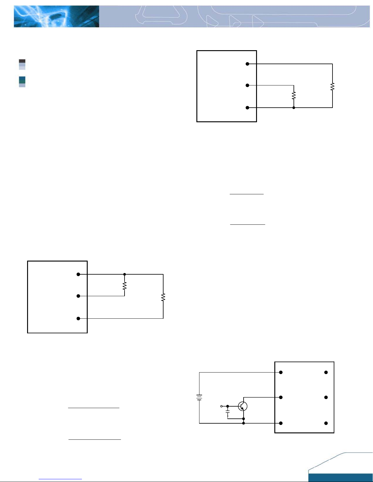
Figure 16: Circuit configuration for trim-down (decrease output
voltage)
If the external resistor is connected between the TRIM
and Vo+ pins, the output voltage set point decreases.
The external resistor value required to obtain a
percentage of output voltage change △Vo% is defined
as:
Vo4.248732.222
downRtrim
=− 32.3
∆−
07.0Vo12
+∆
Ex. When trim-down –10% (12V X 0.9 =10.8V)
×−
=− 50.15232.3
downRtrim
+×
1.04.248732.222
07.01.012
trim-down
[]
ΚΩ−
[]
ΚΩ=−
Vo(+)
Trim
R
trim-up
Vo(-)
Figure 17: Circuit configuration for trim-up (increase output
voltage)
If the external resistor is connected between the TRIM
and Vo - the output voltage set point increases. The
external resistor value required to obtain a percentage
output voltage change △Vo% is defined as:
=− 32.3
upRtrim
Ex. When trim-up +10% (12V X 1.1 = 13.2V)
=− 39.1932.3
upRtrim
Care should be taken to ensure that the maximum
output power of the module remains at or below the
maximum rated power.
668.25
−∆
07.0Vo12
668.25
−×
07.01.012
[]
ΚΩ−
[]
ΚΩ=−
Remote ON/OFF
The remote on/off feature on the module can be either
negative or positive logic. Negative logic turns the
module on during a logic low and off during a logic high.
Positive logic turns the modules on during a logic high
and off during a logic low. Remote on/off can be
controlled by an external switch between the on/off
terminal and the Vi(-) terminal. The switch can be an
open collector or open drain. If the remote on/off feature
is not used, please short the on/off pin to Vi(-) for
negative logic and let the pin open for positive logic.
Vi(+) Vo(+)
ON/OFF
Vi(-)
Trim
Vo(-)
Figure 18: Circuit Configuration for Remote ON/OFF
DS_s48SS12001_06082006
8
Page 9
THERMAL CONSIDERATIONS
A
)
Y
Thermal management is an important part of the system
design. To ensure proper, reliable operation, sufficient
cooling of the power module is needed over the entire
temperature range of the module. Convection cooling is
usually the dominant mode of heat transfer.
Hence, the choice of equipment to characterize the
thermal performance of the power module is a wind
tunnel.
Thermal Testing Setup
Delta’s DC/DC power modules are characterized in
heated vertical wind tunnels that simulate the thermal
environments encountered in most electronics
equipment. This type of equipment commonly uses
vertically mounted circuit cards in cabinet racks in which
the power modules are mounted.
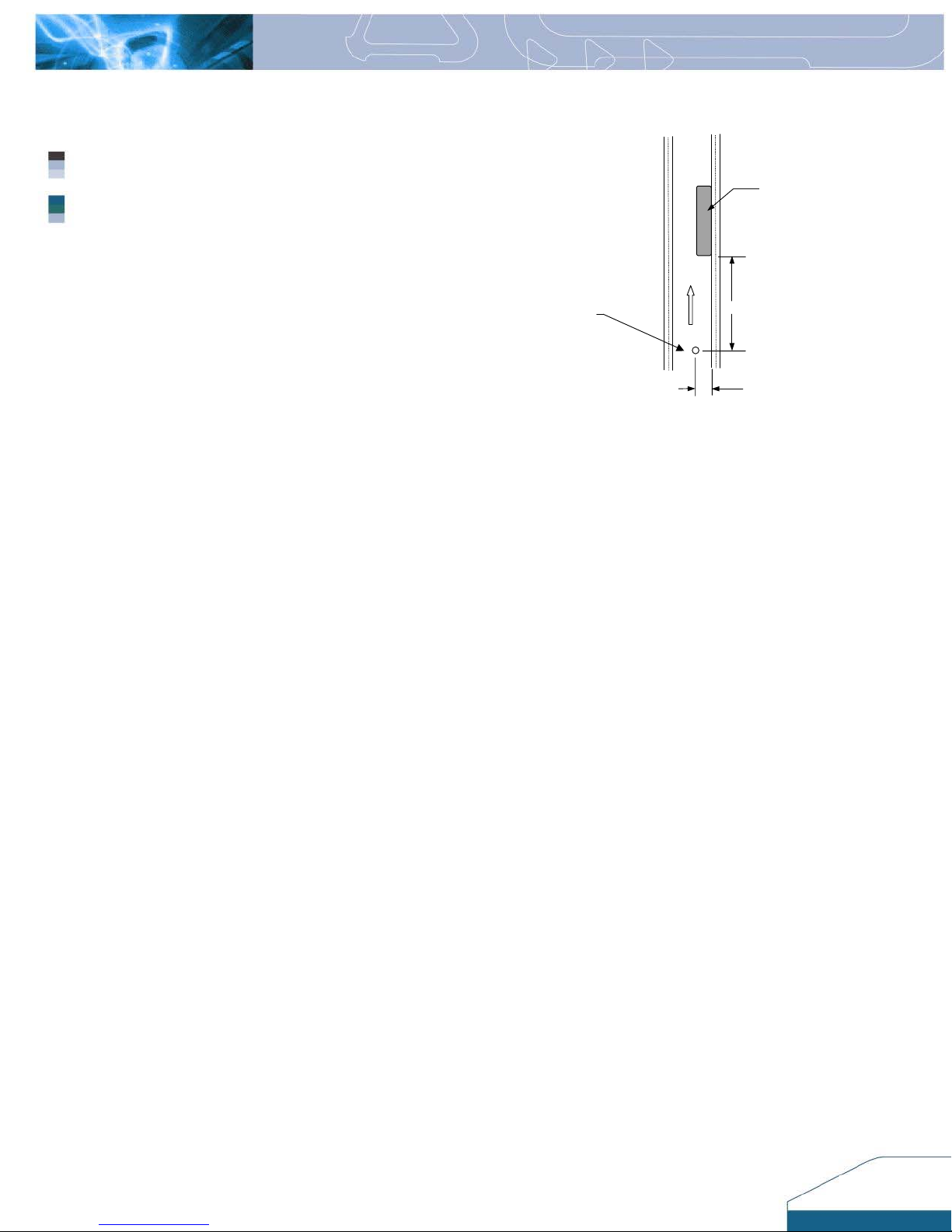
The following figure shows the wind tunnel
characterization setup. The power module is mounted
on a test PWB and is vertically positioned within the
wind tunnel. The space between the neighboring PWB
and the top of the power module or a heat sink is
6.35mm (0.25”).
Thermal Derating
Heat can be removed by increasing airflow over the
module. Figure 13 and 14 show maximum output is a
function of ambient temperature and airflow rate. The
module’s maximum case temperature is +100°C. To
enhance system reliability, the power module should
always be operated below the maximum operating
temperature. If the temperature exceeds the maximum
module temperature, reliability of the unit may be
affected.
TEMPERATURE
MEASURED BELOW
Note: Wind Tunnel Test Setup Figure Dimensions are in millimeters and (Inches)
Figure 19: Wind tunnel test setup
FACING PWB
AIR VELOCIT
AND AMBIENT
THE MODULE
PWB
MODULE
50.8 (2.0”
IR FLOW
10 (0.4”)
DS_s48SS12001_06082006
9
Page 10
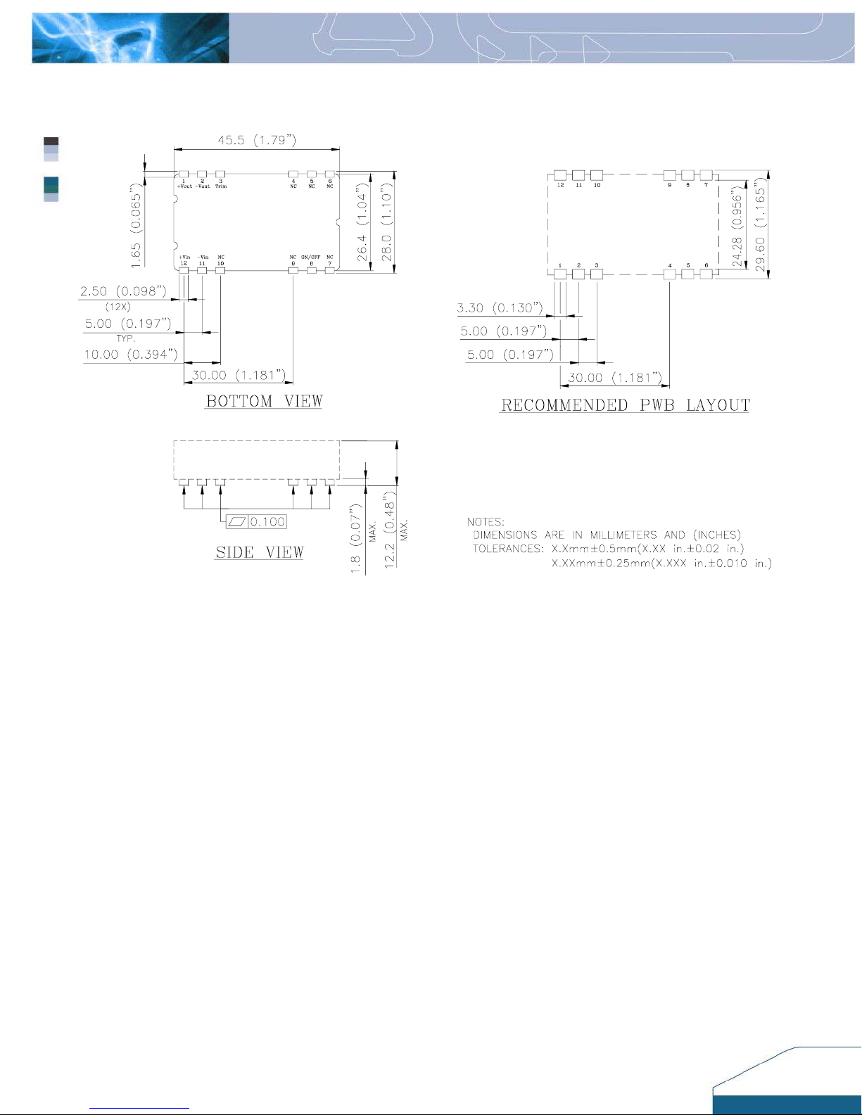
MECHANICAL DRAWING
Pin No. Name Function
1 +Vout Positive output voltage
2 -Vout Negative output voltage
3 Trim Output voltage trim
4 NC No Connection
5 NC No Connection
6 NC No Connection
7 NC No Connection
8 ON/OFF ON/OFF Logic
9 NC No Connection
10 NC No Connection
11 -Vin Negative input voltage
12 +Vin Positive input voltage
DS_s48SS12001_06082006
10
Page 11
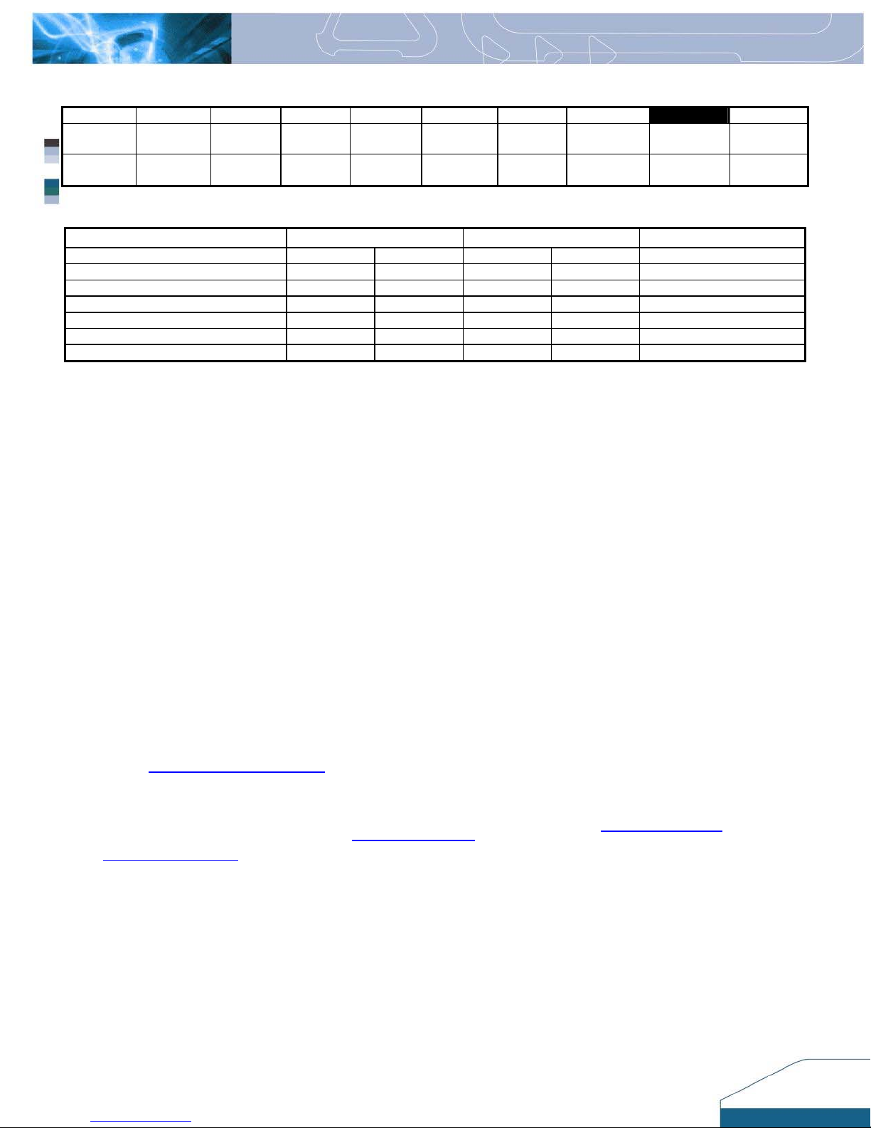
PART NUMBERING SYSTEM
S 48 S S 120 01 N R F A
Form
Factor
S- Small
Power
Input
Voltage
48V-
36V~75V
Number of
Outputs
S- Single S- SMD 120- 12.0V 01- 1.25A N- Negative
Product
Series
Output
Voltage
Output
Current
ON/OFF
Logic
P- Positive
Pin Length Option
Code
R- SMD Pin
F- RoHS 6/6
(Lead Free)
A- Standard
Function
MODEL LIST
MODEL NAME INPUT OUTPUT EFF @ 100% LOAD
S48SS1R805NRFA 36V~75V 0.5A 1.8V 5.0A 80.0%
S48SS2R504NRFA 36V~75V 0.5A 2.5V 4.5A 83.0%
S48SS3R303NRFA 36V~75V 0.5A 3.3V 3.0A 84.0%
S48SS3R304NRFA 36V~75V 0.6A 3.3V 4.5A 86.0%
S48SS05002NRFA 36V~75V 0.5A 5.0V 2.0A 84.0%
S48SS05003NRFA
S48SS12001NRFA 36V~75V 0.6A 12V 1.25A 86.5%
CONTACT:
USA:
Telephone:
East Coast: (888) 335 8201
West Coast: (888) 335 8208
Fax: (978) 656 3964
Email: [email protected]
www.delta.com.tw/dcdc
WARRANTY
Delta offers a two (2) year limited warranty. Complete warranty information is listed on our web site or is available
upon request from Delta.
Information furnished by Delta is believed to be accurate and reliable. However, no responsibility is assumed by Delta
for its use, nor for any infringements of patents or other rights of third parties, which may result from its use. No license
is granted by implication or otherwise under any patent or patent rights of Delta. Delta reserves the right to revise
these specifications at any time, without notice.
36V~75V 0.6A 5.0V 3.0A 86.5%
Europe:
Phone: +41 31 998 53 11
Fax: +41 31 998 53 53
Email:
Asia & the rest of world:
Telephone: +886 3 4526107 ext 6220
Fax: +886 3 4513485
Email:
DS_s48SS12001_06082006
14
11
 Loading...