

Page 1

S3CB018/FB018 PRODUCT OVERVIEW
1 PRODUCT OVERVIEW
CALMRISC OVERVIEW
The S3CB018/FB018 single-chip CMOS microcontroller is designed for high performance using Samsung’ s
newest 8-bit CPU core, CalmRISC.
CalmRISC is an 8-bit low power RISC microcontroller. Its basic architecture follows Harvard style, that is, it has
separate program memory and data memory. Both instruction and data can be fetched simultaneously without
causing a stall, using separate paths for memory access. Represented below is the top block diagram of the
CalmRISC microcontroller.
1-1
Page 2

PRODUCT OVERVIEW S3CB018/FB018
S3CB018/FB018 OVERVIEW
FEATURES SUMMARY
CPU
• 8-Bit RISC architecture
Memory
• ROM: 4 Kword (8 K-byte)
• RAM: 3072 (1024+2048) byte
1024 (X-memory) byte
2048 (Y-memory) byte
Stack
• size: maximum 16 (word)-level
26 I/O Pins
• I/O: 26 pins, including 8 S/W open drain pins
8-Bit Basic Timer
• Programmable interval timer
• 8 kinds of clock source
Watchdog Timer
• System reset when 11-bit counter overflows
16-Bit Timer/Counter
• Programmable interval timer
• Two 8-bit timer counter mode and one 16-bit
timer counter mode, selectable by S/W
Watch Timer
• Real time clock or interval time measurement
• Four frequency outputs for buzzer sound
8-Bit Serial I/O Interface
• 8-bit transmit/receive mode
• 8-bit receive mode
• LSB first or MSB first transmission selectable
• Internal and external clock source
16-Bit Serial I/O Interface
• 16-bit transmit/receive mode
• External clock source
Coprocessor
• MAC 816
• 8 x 16, 16 x 16 Multiply and Accumulation
• Arithmetic operation
Two Power-Down Modes
• Idle mode: only CPU clock stop
• Stop mode: selected system clock and CPU
clock stop
Oscillation Sources
• Crystal and Ceramic (0.4-20MHz), RC
Oscillation
• Programmable oscillation source
Instruction Execution Times
• 50ns at 20MHz for 1 cycle instruction
• 100ns at 20MHz for 2 cycle instruction
1-2
Page 3
S3CB018/FB018 PRODUCT OVERVIEW
DO[7:0]
DI[7:0]
PA[19:0]
PD[15:0]
Program Memory Address
Generation Unit
TBH TBL
ABUS[7:0]
ALUL ALUR
ALU
PC[19:0]
20
HS[0]
Hardware
Stack
HS[15]
BBUS[7:0]
Flag
RBUS
20
8
8
R0
R1
R2
R3
GPR
DA[15:0]
ILHILX ILL
Data Memory
Address
Generation Unit
Bank 0,1
IDH
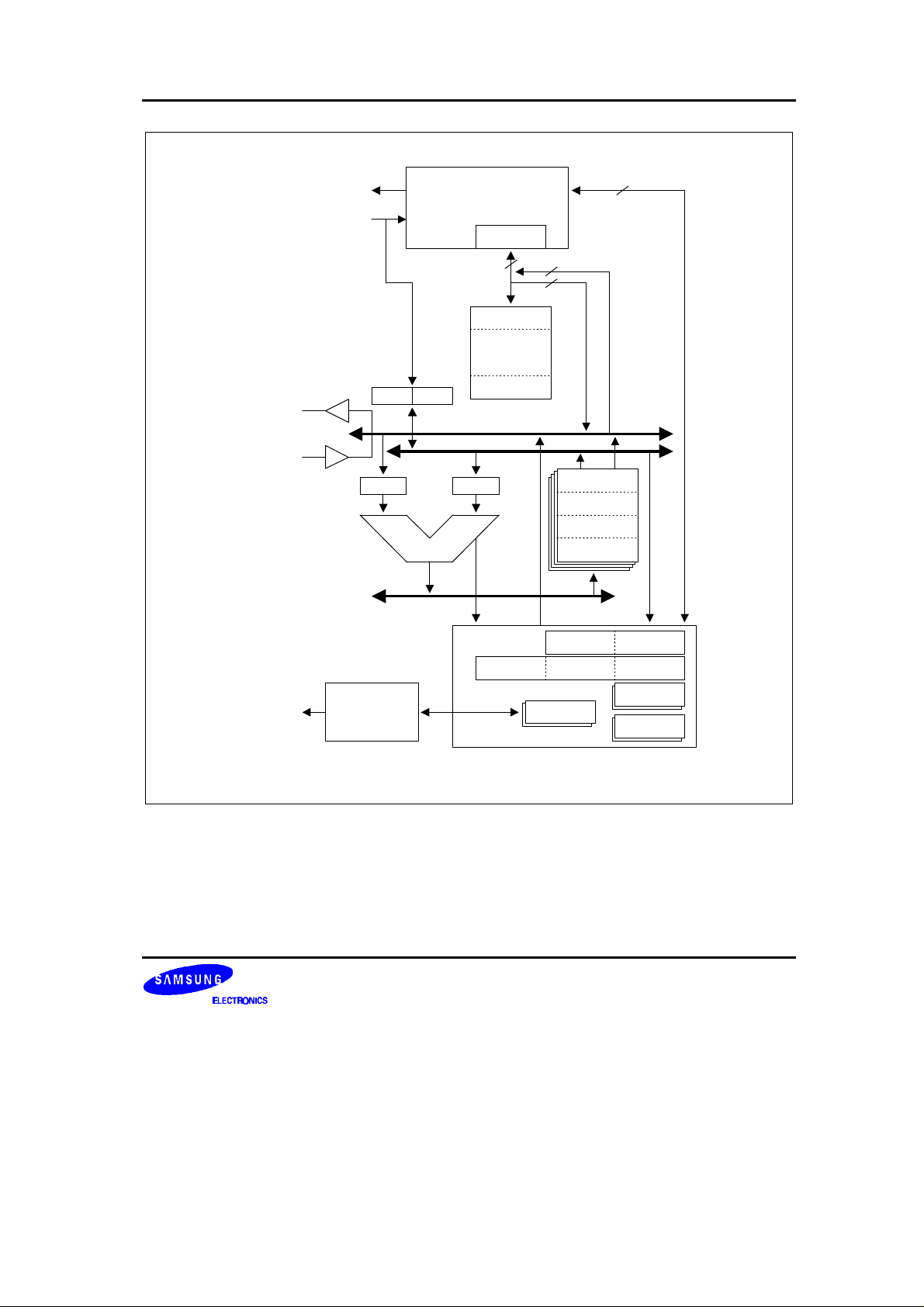
Figure 1-1. Top Block Diagram of CalmRISC
SR0SR1
IDL0
IDL1
SPR
1-3
Page 4
PRODUCT OVERVIEW S3CB018/FB018
The CalmRISC building blocks consist of:
— An 8-bit ALU
— 16 general purpose registers (GPR)
— 11 special purpose registers (SPR)
— 16-level hardware stack
— Program memory address generation unit
— Data memory address generation unit
16 GPR’ s are grouped into four banks (Bank0 to Bank3) and each bank has four 8-bit registers (R0, R1, R2, and
R3). SPR’ s, designed for special purposes, include status registers, link registers for branch-link instructions, and
data memory index registers. The data memory address generation unit provides the data memory address
(denoted as DA[15:0] in the top block diagram) for a data memory access instruction. Data memory contents are
accessed through DI[7:0] for read operations and DO[7:0] for write operations. The program memory address
generation unit contains a program counter, PC[19:0], and supplies the program memory address through
PA[19:0] and fetches the corresponding instruction through PD[15:0] as the result of the program memory access.
CalmRISC has a 16-level hardware stack for low power stack operations as well as a temporary storage area.
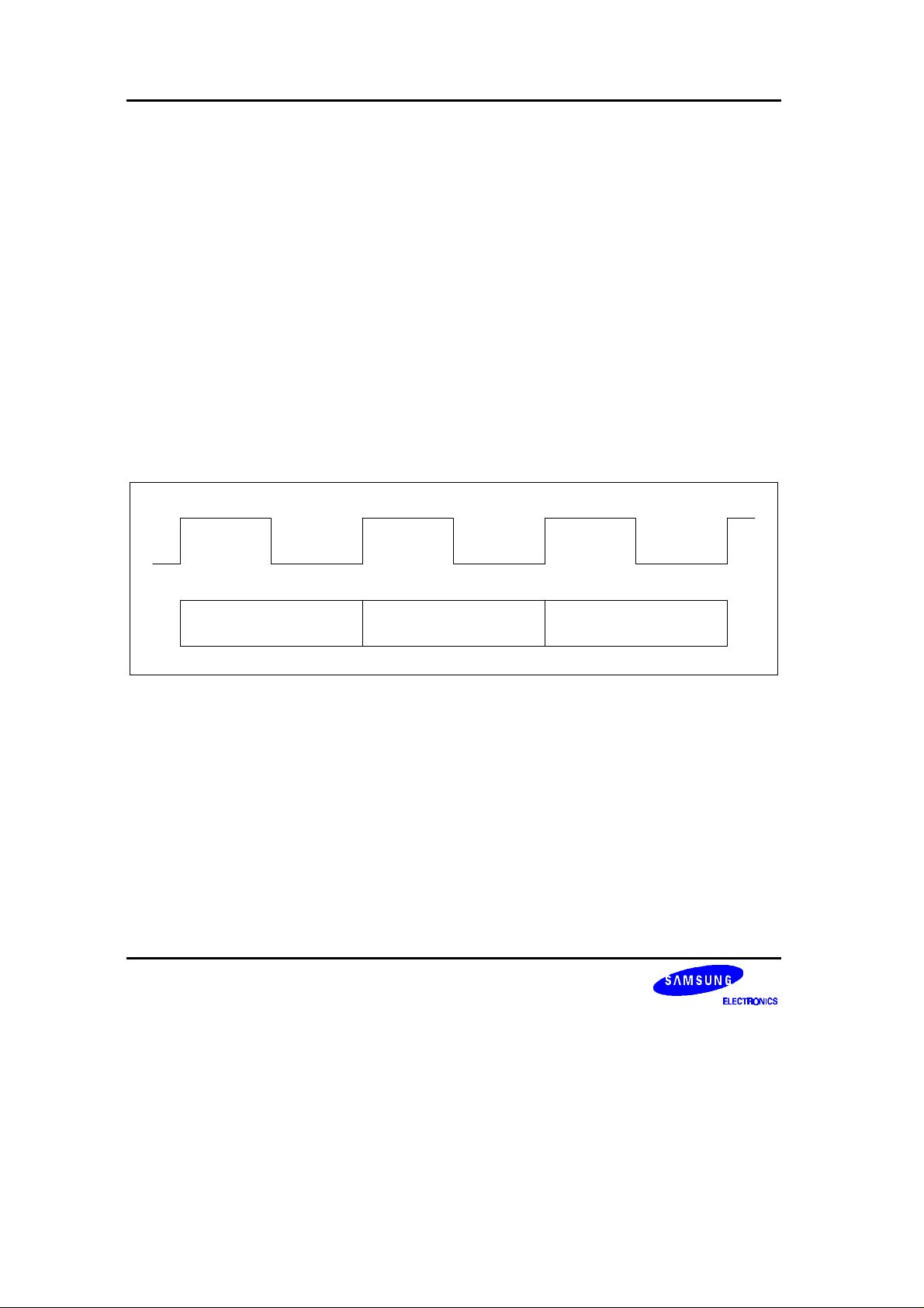
CalmRISC has a 3-stage pipeline as described below:
Instruction Fetch
(IF)
Instruction Decode/
Data Memory Access
(ID/MEM)
Execution/Writeback
(EXE/WB)
Figure 1-2. CalmRISC Pipeline Diagram
As can be seen in the pipeline scheme, CalmRISC adopts a register-memory instruction set. In other words, data
memory where R is a GPR, can be one operand of an ALU instruction as shown below:
The first stage (or cycle) is Instruction Fetch stage (IF for short), where the instruction pointed to by the program
counter, PC[19:0] , is read into the Instruction Register (IR for short). The second stage is Instruction Decode and
Data Memory Access stage (ID/MEM for short), where the fetched instruction (stored in IR) is decoded and data
memory access is performed, if necessary. The final stage is Execute and Write-back stage (EXE/WB), where the
required ALU operation is executed and the result is written back into the destination registers.
Since CalmRISC instructions are pipelined, the next instruction fetch is not postponed until the current instruction
is completely finished, but is performed immediately after the current instruction fetch is done. The pipeline stream
of instructions is illustrated in the following diagram.
1-4
Page 5

S3CB018/FB018 PRODUCT OVERVIEW
/ 1
ID/MEM
/ 2
EXE/WBIF
IF
ID/MEM
/ 3
IF
/ 4
EXE/WB
ID/MEM
IF IF
EXE/WB
/ 5
ID/MEM
IF
/ 6
EXE/WB
ID/MEM
IF
EXE/WB
ID/MEM
EXE/WB
Figure 1-3. CalmRISC Pipeline Stream Diagram
Most CalmRISC instructions are 1-word instructions, while same branch instructions such as “LCALL” and “LJT”
instructions are 2-word instructions. In Figure 1-3, the instruction, I4, is a long branch instruction and it takes two
clock cycles to fetch the instruction. As indicated in the pipeline stream, the number of clocks per instruction (CPI)
is 1 except for long branches, which take 2 clock cycles per instruction.
1-5
Page 6

PRODUCT OVERVIEW S3CB018/FB018
P3.0 - P3.1
P2.0 - P2.7
P1.0 - P1.7
P0.0 - P0.7
Port 3
Port 2
Port 1
Port 0
OSC
Control
X-Memory
1024 Byte
MAC
816
WT BT/WDT
CalmRISC
CPU
Y-Memory
2048 Byte
Control Register
128 Byte
(38 Byte)
Figure 1-4. S3CB018/FB018 Block Diagram
SIO
Timer A
Timer B
SIO
SI
S0
SCK
TACLK
TAOUT
TBCLK
TBOUT
ADDA
1-6
Page 7
S3CB018/FB018 PRODUCT OVERVIEW
PIN ASSIGNMENTS
VSS
XOUT
X
TEST
SI/P0.0
SO/P0.1
RESET
SCK/P0.2
BUZ/P0.3
CSI/P0.4
CSO/P0.5
CSCK/P0.6
CFSYNC/P0.7
CFSYNC/P0.7
P1.0
P1.1
P1.7
VSS
X
OUT
XIN
TEST
SI/P0.0
SO/P0.1
RESET
SCK/P0.2
BUZ/P0.3
CSI/P0.4
CSO/P0.5
CSCK/P0.6
P1.0
P1.1
1
2
3
IN
4
5
6
7
8
9
10
11
12
13
14
15
16
S3CB018
32-SOP
(Top-View)
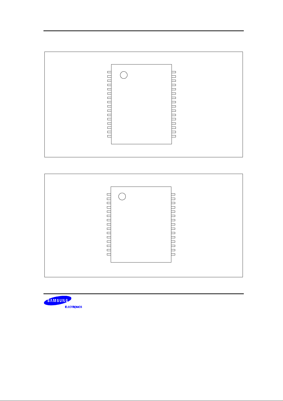
Figure 1-5. 32-SOP Pin Assignment
1
2
3
4
5
6
7
8
9
10
11
12
13
14
15
S3CB018
30-SDIP
(Top View)
VDD
32
P3.1/SCLK/INT01
31
P3.0/SDAT/INT00
30
P2.7/TACLK
29
P2.6/TBOUT
28
P2.5/TBCLK
27
P2.4/TAOUT
26
P2.3/INT13
25
P2.2/INT12
24
P2.1/INT11
23
P2.0/INT10
22
P1.2
21
P1.3
20
P1.4
19
P1.5
18
P1.6
17
VDD
30
P3.1/SCLK/INT01
29
P3.0/SDAT/INT00
28
P2.7/TACLK
27
P2.6/TBOUT
26
P2.5/TBCLK
25
P2.4/TAOUT
24
P2.3/INT13
23
P2.2/INT12
22
P2.1/INT11
21
P2.0/INT10
20
P1.2
19
P1.3
18
P1.4
17
P1.5
16
Figure 1-6. 30-SDIP Pin Assignment
1-7
Page 8

PRODUCT OVERVIEW S3CB018/FB018
I/O PIN DESCRIPTION
Table 1-1. S3CB018/FB018 Pin Descriptions (32-SOP)
Pin
Name
Pin
Type
P0.0-P0.7 I/O I/O port with bit programmable pins; Input and output mode are
selectable by software; Software assignable pull-up. P0.4-P0.7
can be used as inputs for comparator input CIN0-CIN3.;
Alternately they can be used as SI, SO, SCK, BUZ, CSI, CSO,
CSCK, CFSYNC.
P1.0-P1.7 O Output port with bit programmable pins; Push-pull output mode
and open-drain output mode are selected by software;
Software assignable pull-up.
P2.0-P2.7 I/O I/O port with bit programmable pins; Input and output mode are
selectable by software; Software assignable pull-up; P2.0-P2.3
can be used as inputs for external interrupts INT10-INT13.
(with noise filter) ; Alternately they can be used as TAOUT,
TACLK or TBOUT, TBCLK.
P3.0-P3.1 I/O I/O port with bit programmable pins; Input or output mode
selected by software; software assignable pull-up; P3.0-P3.1
can be used as inputs for external interrupts INT00-INT01.
(with noise filter and interrupt polarity control)
Pin Description
Circuit
Type
D-2
F-10
Share
Pins
SI, SO, SCK
BUZ, CSI,
CSO, CSCK,
CFSYNC
E-2
D-4
INT10-INT13
D-2
TAOUT
TACLK
TBOUT
TBCLK
D-4 INT00-INT01
Table 1-2. S3CB018/FB018 Pin Descriptions (30-SDIP)
Pin
Name
Pin
Type
Pin Description Circuit
P0.0-P0.7 I/O I/O port with bit programmable pins; Input and output mode are
selectable by software; Software assignable pull-up. P0.4-P0.7
can be used as SI, SO, SCK, BUZ, CSI, CSO, CSCK,
CFSYNC, Alternately.
P1.0-P1.5 O O port with bit programmable pins; Push-pull output mode and
open-drain output mode are selected by software; Software
assignable pull-up.
P2.0-P2.7 I/O I/O port with bit programmable pins; Input and output mode are
selectable by software; Software assignable pull-up; P2.0-P2.3
can be used as inputs for external interrupts INT10-INT13.
(with noise filter); Alternately they can be used as TAOUT,
TACLK or TBOUT, TBCLK.
P3.0-P3.1 I/O I/O port with bit programmable pins; Input or output mode
selected by software; software assignable pull-up; P3.0-P3.1
can be used as inputs for external interrupts INT00-INT01.
(with noise filter and interrupt polarity control)
NOTE: In S3CB018/FB018, the CSI, CSO, CSCK, CFSYNC pins are shared with P0.7-P0.4.
Share
Type
D-2
F-10
Pins
SI, SO, SCK
BUZ, CSI,
CSO, CSCK,
CFSYNC
E-2
D-4
INT10-INT13
D-2
TAOUT
TACLK
TBOUT
TBCLK
D-4 INT00-INT01
1-8
Page 9
S3CB018/FB018 PRODUCT OVERVIEW
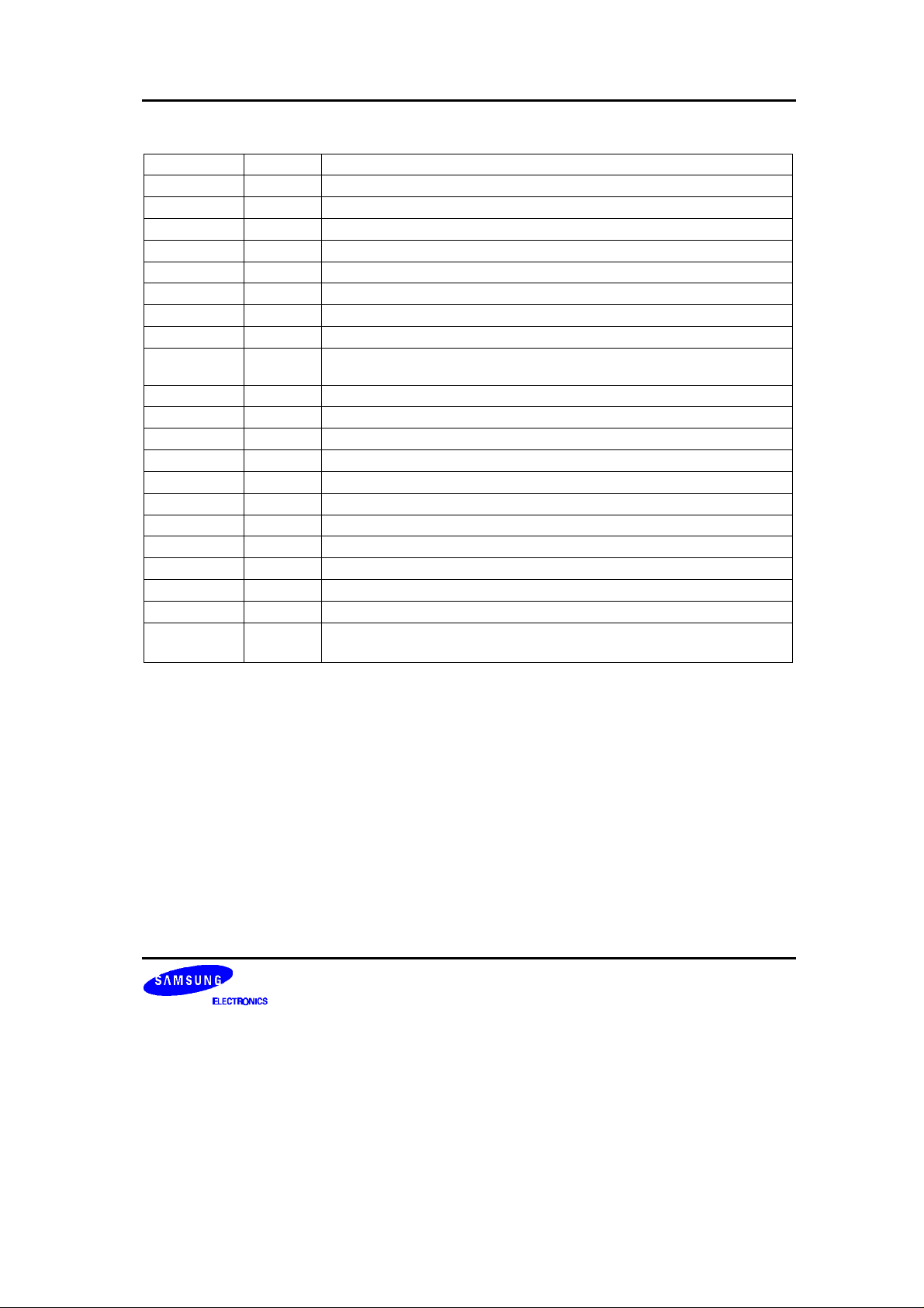
Table 1-3. I/O Pin Description
Pin Name Pin Type Description
CSI I AD/DA Serial Input (from codec)
CSO O AD/DA Serial Output (to codec)
CSCK I AD/DA Serial Clock (from codec)
CFSYNC I AD/DA Sync signal (from codec)
SI I/O Serial data input
SO I/O Serial data output
SCK I/O Serial I/O interface clock signal
BUZ I/O 0.5 kHz, 1 kHz, 2 kHz, or 4 kHz frequency output at 4.19 MHz for buzzer sound
INT10-INT13 I External interrupts. Stop release. Can’ t be masked by S/W individually but
wholly.
TAOUT I/O Timer A interval mode output
TACLK I/O Timer A counter external clock input
TBOUT I/O Timer B interval mode output
TBCLK I/O Timer B counter external clock input
INT00-INT01 I External interrupts. Stop release. Can be masked by S/W individually.
SDAT I Serial data for Programmable memory
SCLK I Serial clock for Programmable memory
VDD – Power supply
VSS – Ground
TEST – Test signal input
RESET I Reset signal
XIN, X
OUT
– Crystal, ceramic and RC oscillator signal for system clock (For external clock
input, use XIN and input XIN's reverse phase to X
OUT
)
1-9
Page 10
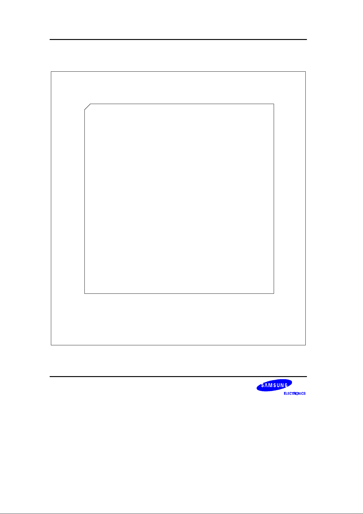
PRODUCT OVERVIEW S3CB018/FB018
PIN ASSIGNMENTS
P0.0
P0.1
P0.2
V
P0.3
P0.4
P0.5
GND
P0.6
P0.7
V
P1.0
P1.1
P1.2
P1.3
GND
P1.4
P1.5
P1.6
P1.7
GND
X
XOUT
V
DDI/VDD
P2.0
P2.1
P2.2
V
P2.3
P2.4
GND
P2.5
P2.6
P2.7
VDD
P3.0
P3.1
GND
TMODE
PIN_RESB
CFSYNC
CSOUT
CSCLK
CSIN
V
DD
156
157
158
159
160
1
2
3
4
DD
5
6
7
8
9
10
11
DD
12
13
14
15
16
17
18
19
20
21
22
IN
23
24
25
26
27
28
DD
29
30
31
32
33
34
35
36
37
38
39
40
45
44
434241
PTMS
PTCK_MCLK
V
PNTRST_STATEINIT
JTAGSEL
DD
/V
DDI
EVENIO
WENIO
OENIO
153
154
155
484746
GND
PTDO_TXD
PTDI_RXD
CSNWIO
CSNBIO
GND
150
151
152
50
49
NPMCS
NPMOE
NPMWE
WENX
OENX
148
149
535251
VDD
RUNST
VDD/VDDI
CSNXH
CSNXL
XD15
144
145
146
147
(Top-View)
57
565554
NP64KW
XDOCNT
DOCNTX
OUTDIS
XD10
XD11
XD12
XD13
XD14
GND
138
139
140
141
142
143
S3EB010
160-QFP
636261
605958
PD12
PD13
VDD/VDDI
PD14
PD15
GND
XD9
137
64
PD11
XD8
136
65
GND
V
DD
135
66
PD10
XD7
134
67
PD9
XD6
133
68
PD8
XD5
132
69
V
DD
/V
DDI
XD4
131
70
PD7
GND
130
71
PD6
XD3
129
72
PD5
XD2
128
73
PD4
XD1
127
GND
XD0
126
PD3
VDD
125
767574
PD2
XDA1
XDA0
123
124
78
77
PD0
PD1
XDA3
XDA2
121
122
80
79
ICLKO
GND
120
119
118
117
116
115
114
113
112
111
110
109
108
107
106
105
104
103
102
101
100
99
98
97
96
95
94
93
92
91
90
89
88
87
86
85
84
83
82
81
XDA4
XDA5
XDA6
GND
XDA7
XDA8
XDA9
VDD/V
DDI
XDA10
XDA11
XDA12
XDA13
GND
TEST
PA0
PA1
PA2
VDD/VDDI
PA3
PA4
PA5
GND
PA6
PA7
V
DD
PA8
PA9
PA10
PA11
GND
PA12
PA13
PA14
PA15
VDD
PA16
PA17
PA18
PA19
BKREQX
1-10
Figure 1-7. S3EB010 Pin Diagram
Page 11
S3CB018/FB018 PRODUCT OVERVIEW
Table 1-4. Evaluation Chip Pin Descriptions
No. Pin Name Pin Type Description
1-3
5-9
12-15
17-20
22
23
25-27
29, 30
32, 34
P0.0-P0.2
P0.3-P0.7
P1.0-P1.3
P1.4-P1.7
X
IN
X
OUT
P2.0-P2.2
P2.3, P2.4
P2.5-P2.7
I/O Port 0
O Port 1
I Clock In
O Clock Out
I/O Port 2
36, 37 P3.0, P3.1 I/O Port 3
39 TMODE I Test Mode pin; 1: skip warm-up time, 0: normal mode
40 PIN_RESB I Asynchronous reset, active low
41 JTAGSEL I JTAG mode select; 1: parallel, 0: serial
42 PNTRST_STSTEINI
I JTAG/UART pin
T
44 PTCK_MCLK I JTAG/UART pin
45 PTMS I JTAG/UART pin
46 PTDI_RXD I JTAG/UART pin
47 PTDO_TXD O JTAG/UART pin
49 NPMWE O Program Memory Write Enable, active low
50 NPMOE O Program Memory Output Enable, active low
51 NPMCS O Program Memory Chip Select, active low
52 RUNST O Run Status Indicator
54 OUTDIS I I/O PAD Disable for debugger
55 DOCNTX I Data Bus Output Control
56 XDOCNTX I External X-Memory Data Bus Output Control
57 NPM64KW I Up to 64KW Program Memory, active low
59, 60
62-64
66-68
70-73
75-78
PD15-PD14
PD13-PD11
PD10-PD8
PD7-PD4
PD3-PD0
I/O Program Memory Data Bus
1-11
Page 12
PRODUCT OVERVIEW S3CB018/FB018
Table 1-4. Evaluation Chip Pin Descriptions (Continued)
No. Pin Name Pin Type Description
80 ICLKO O ICLK Output
81 BKREQX I Break input for debugger
82-85
87-90
92-95
97, 98
100-102
104-106
PA19-PA16
PA15-PA12
PA11-PA8
PA7, PA6
PA5-PA3
PA2-PA0
O Program Memory Address
107 TEST I Test pin for debugger
109-112
114-116
118-124
126-129
131-134
136-138
140-144
XDA13-XDA10
XDA9-XDA7
XDA6-XDA0
XD0-XD3
XD4-XD7
XD8-XD10
XD11-XD15
O External X-Memory Address
I/O External X-Memory Data Bus
146 CSNXH O External X-Memory High Byte Chip Select, active low
147 CSNXL O External X-Memory Low Byte Chip Select, active low
148 WENX O External X-Memory Write Enable, active low
149 OENX O External X-Memory Output Enable, active low
151 CSNWIO O External I/O Word Chip Select, active low
152 CSNBIO O External I/O Byte Chip Select, active low
153 EVENIO O External I/O Even Indicator; 1:Even, 0: Odd
154 WENIO O External I/O Write Enable, active low
155 OENIO O External I/O Output Enable, active low
157 CSIN I AD / DA Serial Input (from codec)
158 CSCLK I AD / DA Serial Clock (from codec)
159 CFSYNC I AD / DA Sync signal (from codec)
160 CSOUT O AD / DA Serial Output (to codec)
VDD Power supply – 4, 11, 24, 28, 35, 43, 53, 61, 69, 86, 96, 103, 113
125, 135, 145, 156
GND Ground – 8, 16, 21, 31, 38, 48, 58, 65, 74, 79, 91, 99, 108, 117
130, 139, 150
1-12
Page 13
S3CB018/FB018 PRODUCT OVERVIEW
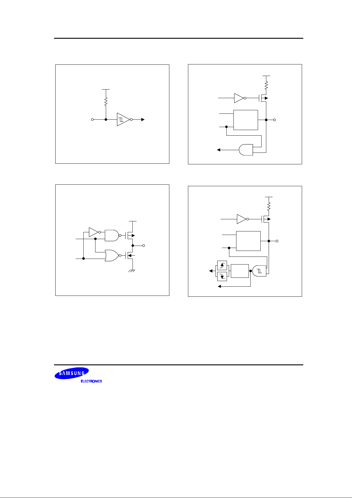
PIN CIRCUIT DIAGRAMS
VDD
V
DD
Pull-Up
Resistor
In
Schmitt Trigger
Pull-up
Enable
Data
Output
Disable
Circuit
Type C
P-Channel
I/O
Figure 1-8. Pin Circuit Type B (RESET)
V
DD
Data
Output
Disable
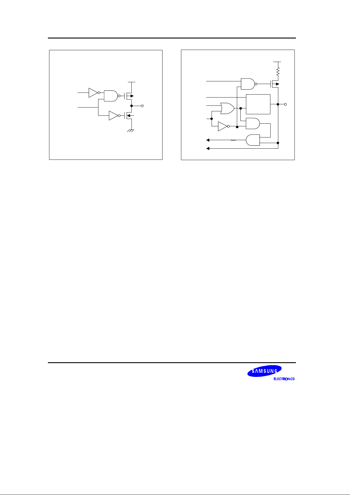
Figure 1-9. Pin Circuit Type C
P-Channel
Out
N-Channel
Figure 1-10. Pin Circuit Type D-2
(P0.0-P0.3, P2.4-P2.7)
V
DD
Pull-up
Enable
Data
Output
Circuit
Type C
P-Channel
I/O
Disable
Noise
Ext. INT
Filter
Schmitt Trigger
Input
Figure 1-11. Pin Circuit Type D-4 (P2.0-P2.3, P3)
1-13
Page 14
PRODUCT OVERVIEW S3CB018/FB018
VDD
Open-drain
Enable
Data
Figure 1-12. Pin Circuit Type E-2 (P1)
VDD
P-Channel
Out
N-Channel
Pull-up
Enable
Data
Output
Disable
Circuit
Type C
Comparator
Enable
Input
Reserved
Figure 1-13. Pin Circuit Type F-10 (P0.4-P0.7)
I/O
1-14
Page 15
S3CB018/FB018 ELECTRICAL DATA
18 ELECTRICAL DATA
OVERVIEW
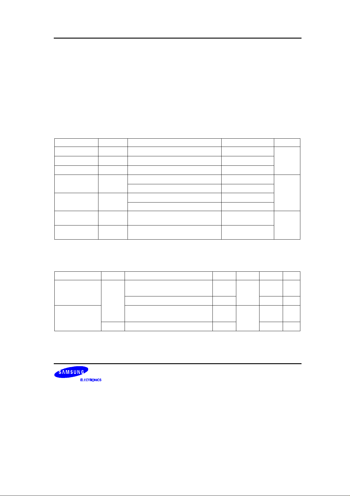
Table 18-1. Absolute Maximum Ratings
(TA = 25°C)
Parameter Symbol Conditions Rating Unit
T
V
I
I
DD
V
V
OH
OL
T
STG
– – 0.3 to + 6.0 V
I
O
One I/O pin active – 18 mA
One I/O pin active + 30
A
–
–
– – 40 to + 85
– – 65 to + 150
– 0.3 to V
– 0.3 to VDD + 0.3
DD
+ 0.3
°
C
Supply voltage
Input voltage
Output voltage
Output current
high All I/O pins active – 60
Output current
low Total pin current for ports 1, 2, 3 + 100
Operating
temperature
Storage
temperature
Table 18-2. D.C. Electrical Characteristics
(T
= – 40°C to + 85°C, VDD = 1.8 V to 5.5 V)
A
Parameter Symbol Conditions Min Typ Max Unit
Operating Voltage
(HSX mode)
Operating Voltage
(MSX mode)
V
V
DD
DD
F
F
F
F
CPU
CPU
CPU
CPU
= 20 MHz
= 3 MHz
= 10 MHz
= 3 MHz
4.5 – 5.5 V
1.8 5.5
4.5 – 5.5
1.8 5.5
18-1
Page 16
ELECTRICAL DATA S3C
(TA= 40
° °
C, V = 1.8 V to 5.5 V)
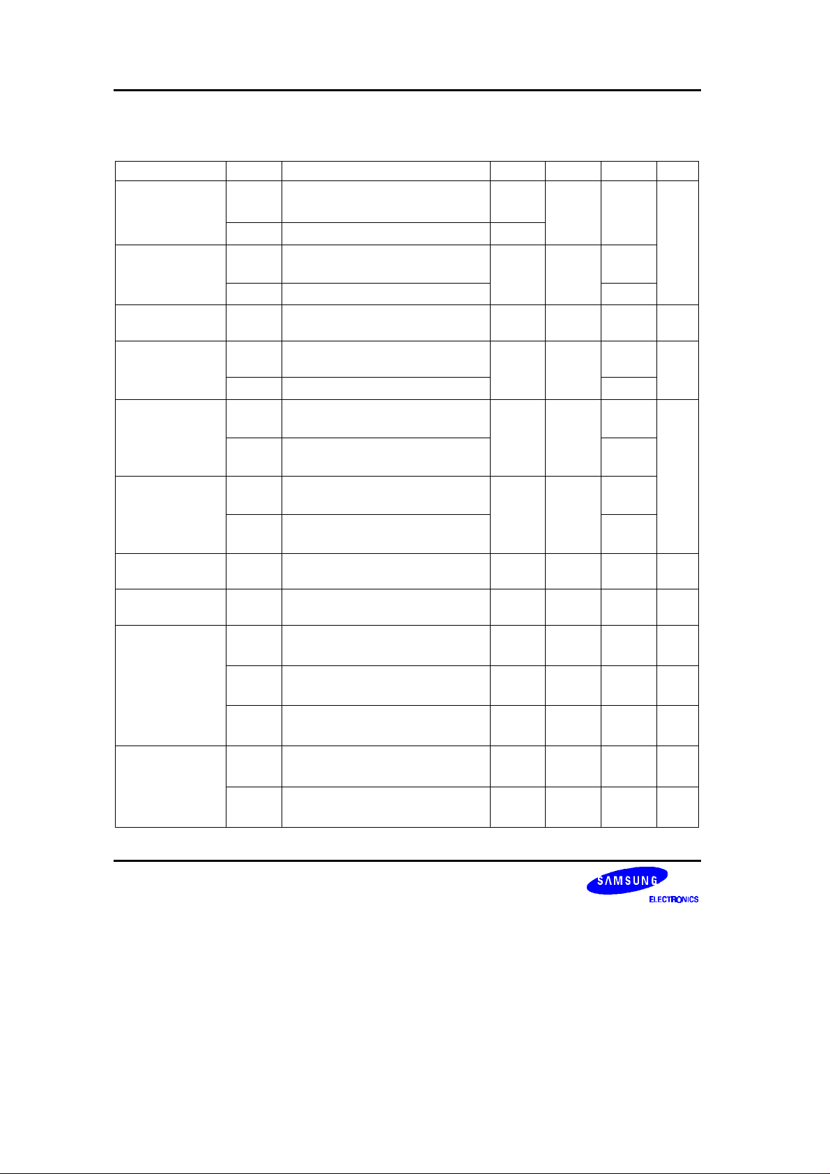
Parameter Conditions Min Max Unit
Input low voltage
Output high voltage
V
IH1 IH2
X V
IH2
V
V
V
All input pins except V
IL1
X
IL2
OH1VDD
IN
= 5V; IOH = -1 mA
IL2
0.8 V
0.1
-
DD
– –
VDD-1.0
–
0.2 V
0.1
– – V
All output pins
Output low voltage
Input high leakage
current
Input low leakage
current
V
OL1VDD
V
OL2VDD
I
LIH1
I
LIH2
I
LIL1
I
LIL2
= 5V; IOL = 8 mA
All output pins except V
= 5V; IOL = 15 mA, Port 1
VIN = V
DD
All input pins except I
VIN = V
DD
XIN, XT
IN
V
= 0 V
IN
All input pins except I
LIH2
LIL2
VIN = 0 V
– 2
OL2
– – 3 uA
20
– – -3
-20
XIN, XTIN, RESET
Output high leakage
current
Output low leakage
current
Oscillator feed back
resistors
Pull-up resistor
I
LOH
I
R
(HSX)
R
(MSX)
R
(LSX)
R
V
= V
OUT
DD
All I/O pins and Output pins
V
LOL
OUT
= 0 V
All I/O pins and Output pins
VDD = 5.0 V, TA = 25°C, XIN = VDD,
osc1
X
= 0V
OUT
VDD = 5.0 V,TA = 25°C, XIN = VDD,
osc2
X
= 0V
OUT
VDD = 5.0 V, TA = 25°C, XIN = VDD,
osc3
X
= 0V
OUT
VIN = 0 V; VDD = 5 V ± 10%
L1
– – 3 uA
– – -3
510 710 910
510 710 910
2.0 2.7 3.5
30 50 70
Ports 0,1,2,3,4,5 TA=25°C
R
L2
VIN = 0 V; V
= 5 V ± 10%
DD
110 210 310
TA=25°C, RESET only
DD
2
V
DD
kΩ
MΩ
kΩ
18-2
Page 17
S3CB018/FB018 ELECTRICAL DATA
Table 18-2. D.C. Electrical Characteristics (Continued)
(T
= – 40°C to + 85°C, VDD = 1.8 V to 5.5 V)
A
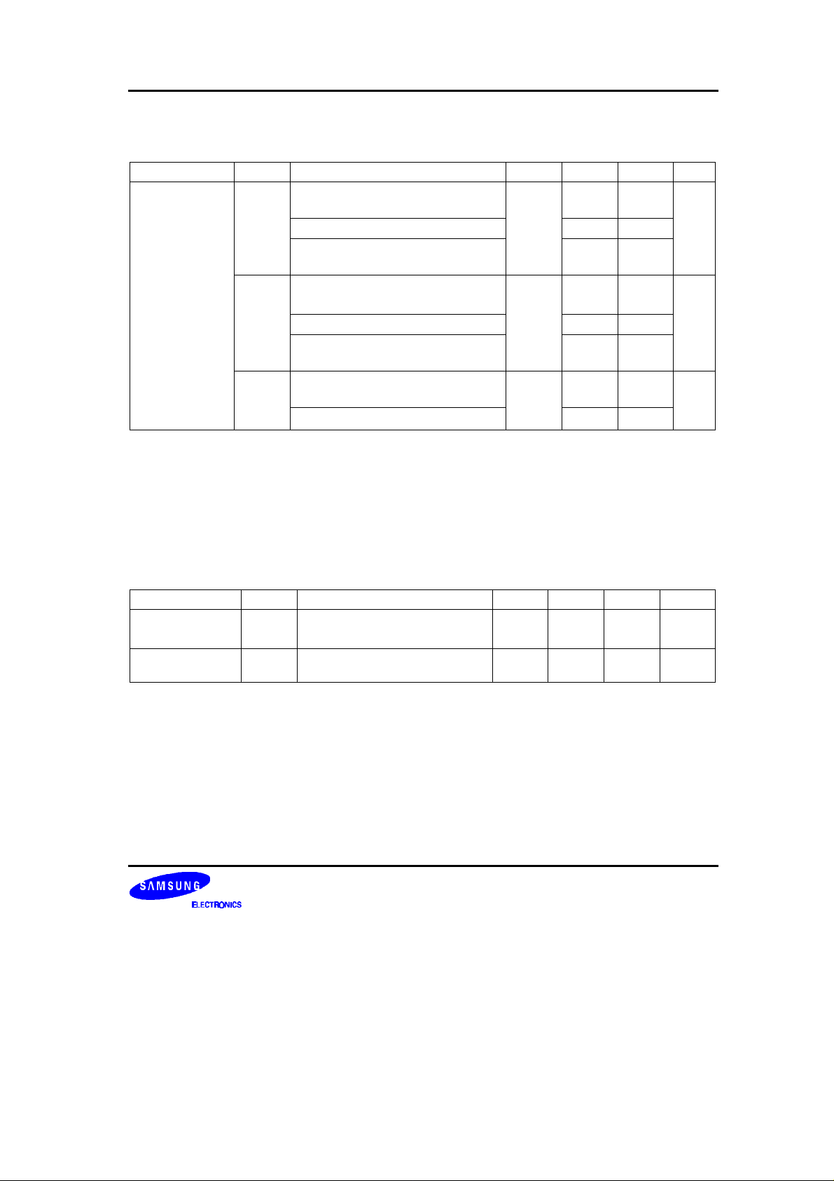
Parameter Symbol Conditions Min Typ Max Unit
Supply current
(1)
I
DD1
(2)
Operating mode: V
= 5 V ± 10%
DD
– 10 20 mA
20 MHz crystal oscillator(HSX)
5 MHz crystal oscillator(MSX)
V
= 3 V ± 10%
DD
4 8
2 4
5 MHz crystal oscillator(MSX)
(3)
I
DD2
Idle mode: VDD = 5 V ± 10%
– 2.5 5 mA
20 MHz crystal oscillator(HSX)
5 MHz crystal oscillator(MSX)
VDD = 3 V± 10%
1 2
0.4 0.8
5 MHz crystal oscillator(MSX)
I
NOTES:
1. Supply current does not include current drawn through internal pull-up resistors or external output current loads.
2. In operating current test mode Timer A and Timer B are running.
3. In idle current test mode the Watch timer is running.
4. The operating and idle currents are measured at weak mode.
DD3
Stop mode
V
= 5 V ± 10%
DD
V
= 3 V ± 10%
DD
– 0.5 3 uA
0.2 1.2
Table 18-3. A. C. Electrical Characteristics
(T
= –40°C to + 85°C, V
A
= 1.8 V to 5.5 V)
DD
Parameter Symbol Conditions Min Typ Max Unit
t
Interrupt input high,
low width
RESET input
low width
NOTE: User must keep a value larger than the min value.
INTH
t
INTL
t
RSL
,
P2.0 - P2.3, P3.0 - P3.1
V
= 5V
DD
V
= 5V ± 10%
DD
200 – – ns
1 – – us
18-3
Page 18
ELECTRICAL DATA S3CB018/FB018
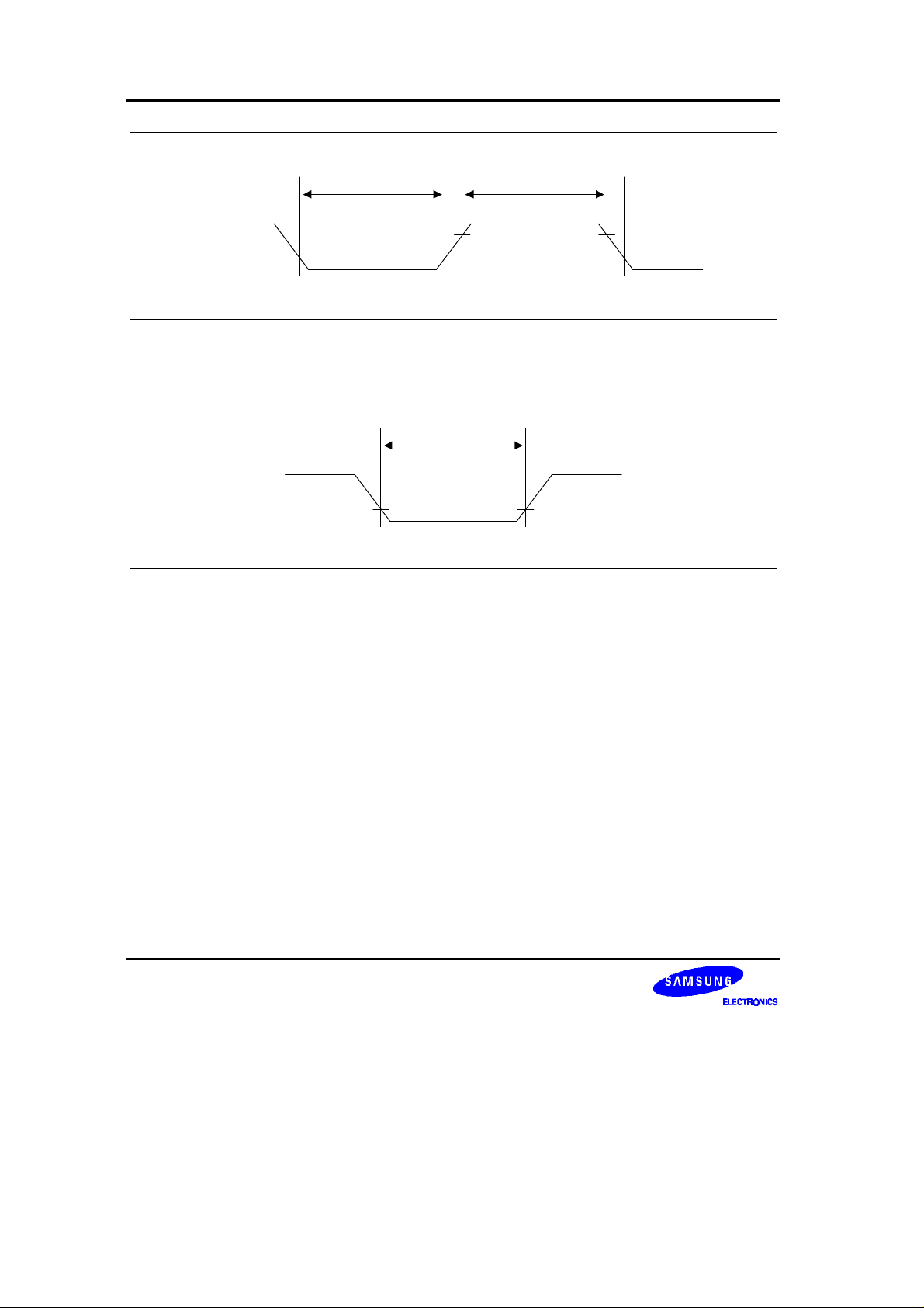
t
INTL
t
INTH
0.8 VDD
0.2 VDD
Figure 18-1. Input Timing for External Interrupts
t
RSL
RESET
0.2 VDD
Figure 18-2. Input Timing for RESET
18-4
Page 19
S3CB018/FB018 ELECTRICAL DATA
Table 18-4. Data Retention Supply Voltage in Stop Mode
(TA = – 40°C to + 85°C, V
= 1.8 V to 5.5V)
DD
Parameter Symbol Conditions Min Typ Max Unit
Data retention
supply voltage
Data retention
supply current
NOTE: Supply current does not include current drawn through internal pull-up resistors or external output current loads.
VDD
RESET
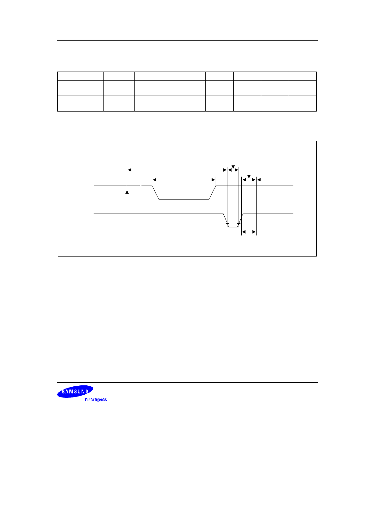
NOTE: t
V
DDDR
I
DDDR
Execution of
STOP Instruction
WAIT
V
= 1.5V
DDDR
~
~
~
~
is the same as 2048 x 32 x 1/fxx
Stop Mode
Data Retention Mode
VDDDR
1.5 – 5.5 V
– – 2 µA
RESET
Occur
Oscillation
Stabilization Time
Normal
Operating Mode
0.2VDD
tWAIT
Figure 18-3. Stop Mode Release Timing When Initiated by a RESET
18-5
Page 20
ELECTRICAL DATA S3CB018/FB018
Oscillation
Stabilization Time
t
WAIT
Normal
Operating
Mode
VDD
INT
NOTE:
Osc Start
up time
~
~
~
~
Execution of
STOP Instruction
t
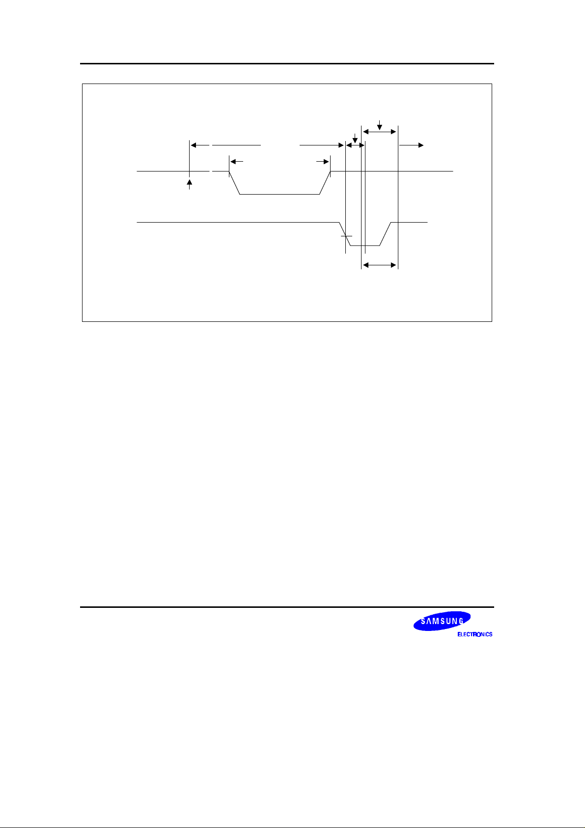
is the same as 2048 x 32 x 1/fxx. The value of 2048 which is selected for the clock
WAIT
source of the basic timer counter can be changed. Then the value of tWAIT will be changed
and ,when you select 16 instead of 32, the value of twait will also be changed.
Stop Mode
Data Retention
V
DDDR
0.2VDD
Figure 18-4. Stop Mode Release Timing When Initiated by Interrupts
18-6
Page 21
S3CB018/FB018 ELECTRICAL DATA
Table 18-5. Synchronous SIO Electrical Characteristics
(TA = – 40°C to + 85°C VDD = 4.5 V to 5.5 V, VSS = 0 V, fxx = 10 MHz oscillator )
Parameter Symbol Conditions Min Typ Max Unit
SCK Cycle time
Serial Clock High
Width
Serial Clock Low
Width
Serial Output data
delay time
Serial Input data
setup time
Serial Input data
Hold time
t
CYC
t
SCKH
t
SCKL
t
OD
t
ID
t
IH
– 200 – – ns
– 60 – –
– 60 – –
– – – 50
– 40 – –
– 100 – –
tCYC
SCK
SO
SCKL
t
tID tIH
SI
tOD
Input Data
Output Data
SCKH
t
DD
0.8 V
0.2 VDD
0.8 V
0.2 V
DD
DD
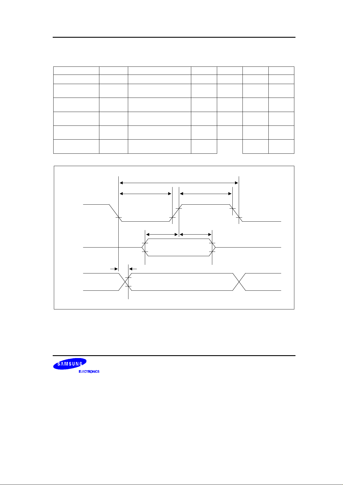
Figure 18-5. Serial Data Transfer Timing
18-7
Page 22
ELECTRICAL DATA S3CB018/FB018
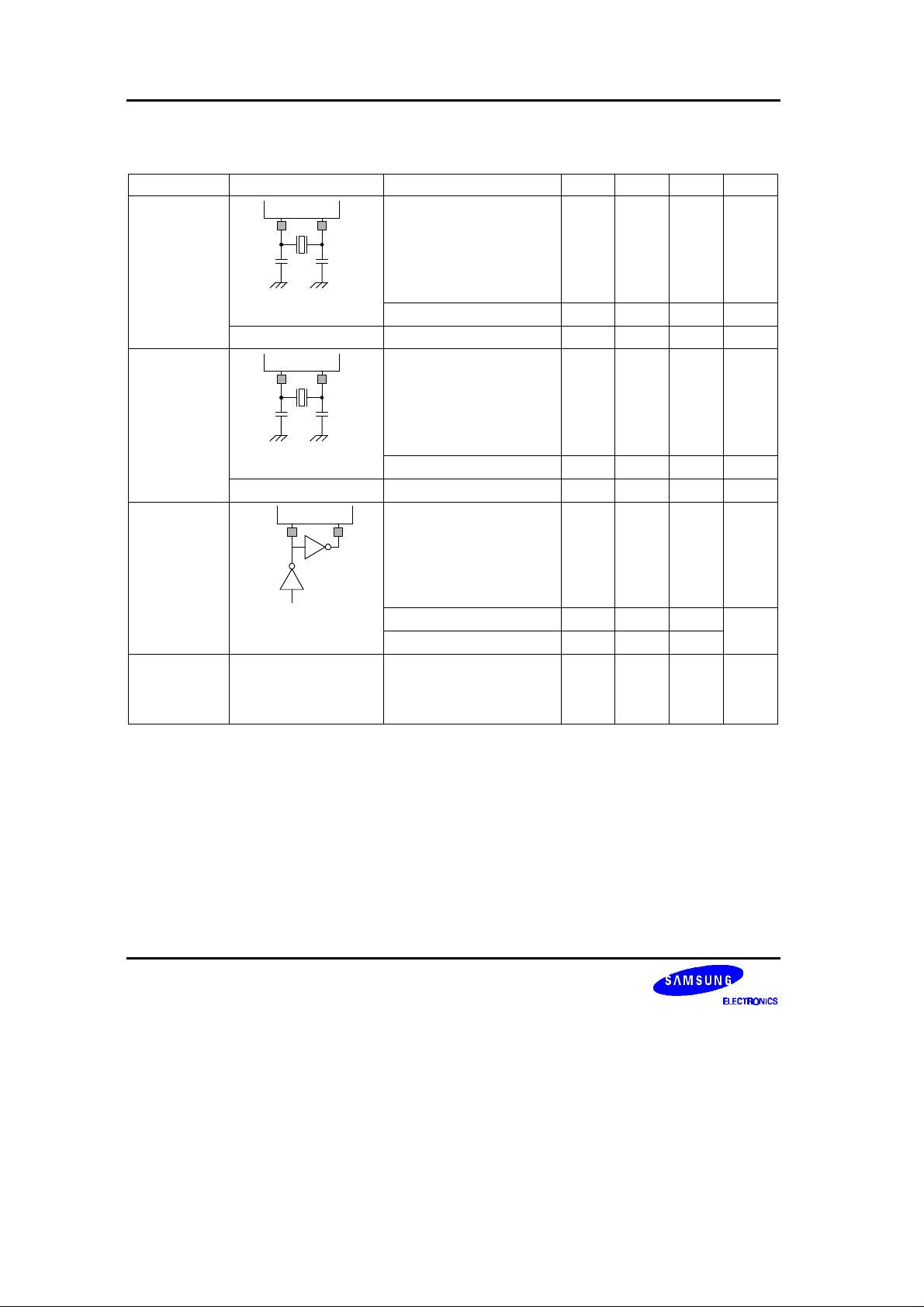
Table 18-6. Main Oscillator Frequency
(T
= -40°C + 85°C, VDD = 1.8 V to 5.5 V)
A
Oscillator Clock Circuit Test Condition Min Typ Max Unit
Crystal
XIN
C1 C2
XOUT
LSX mode 32 32.768 35 kHz
MSX mode 0.4 – 10 MHz
HSX mode 0.4 – 20
Ceramic
XIN
C1 C2
XOUT
LSX mode 32 32.768 35 kHz
MSX mode 0.4 – 10 MHz
HSX mode 0.4 – 20
External clock XIN XOUT LSX mode 32 32.768 35 kHz
MSX mode 0.4 – 10 MHz
HSX mode 0.4 – 20
RC
r = 22Kohm, VDD = 5 V
Direct soldering
NOTES:
1. Keep the wiring length as short as possible.
2. Do not cross the wiring with the other signal lines.
3. Do not route the wiring near a signal line through which a high fluctuating current flows.
4. Always make the ground point of the oscillator capacitor the same potential as VSS.
5. Do not ground the capacitor to a ground pattern through which a high current flows.
6. Do not fetch signals from the oscillator.
18-8
1.4 2 2.6 MHz
Page 23
S3CB018/FB018 ELECTRICAL DATA
3000
2500
2000
1500
1000
Frequency [kHz]
500
0
1.8
15K
22K
30K
33K
36K
62K
82K
120K
180K
300K
2V 3V 4V 5V 5.5V 6V
VDD [V]
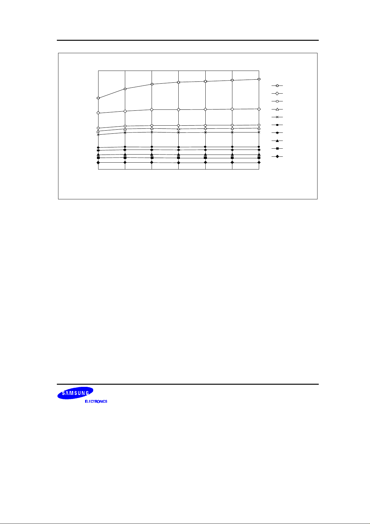
Figure 18-6. RC Oscillator Characteristic Curve
18-9
Page 24
ELECTRICAL DATA S3CB018/FB018
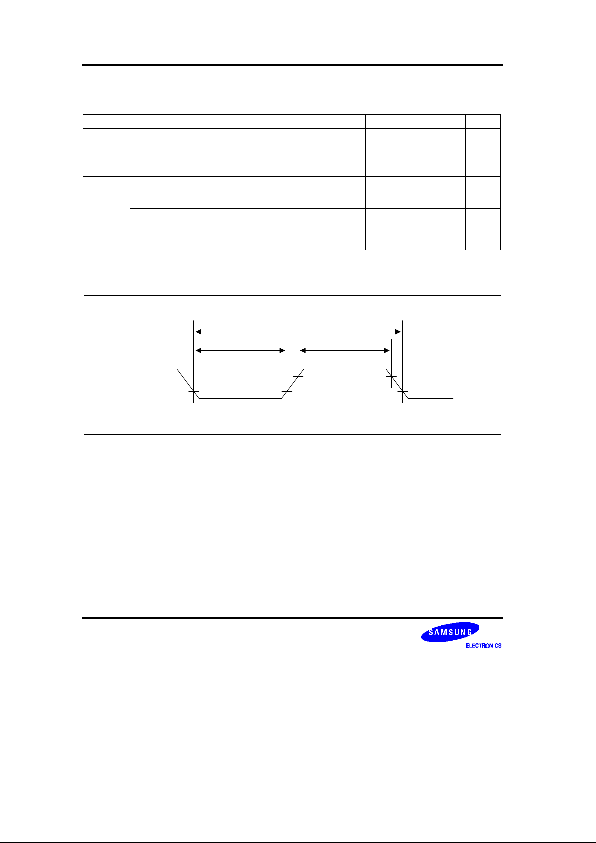
Table 18-7. Main Oscillator Oscillation Stabilization Time (t
(T
= -40°C + 85°C, VDD = 4.5 V to 5.5 V)
A
Oscillator Test Condition(Normal mode) Min Typ Max Unit
HSX Crystal
VDD = minimum oscillation voltage range.
Ceramic – – 4 ms
External clock
MSX Crystal
XIN input high and low level width (tXH, tXL)
VDD = minimum oscillation voltage range.
Ceramic – – 50 ms
External clock
LSX 32768Hz
XIN input high and low level width (tXH, tXL)
VDD = minimum oscillation voltage range.
Crystal
NOTE: Oscillation stabilization time (t
release.
XIN
ST1
)
ST1
– – 10 ms
50 – – ns
– – 100 ms
50 – – ns
– 200 500 ms
) is the time that is required to stabilize oscillation after a reset or STOP mode
1/fosc1
tXHtXL
DD
V
- 0.1 V
0.1 V
18-10
Figure 18-7. Clock Timing Measurement at X
IN
Page 25
S3CB018/FB018 ELECTRICAL DATA
f
CPU
20 MHz
B
10 MHZ
A
3 MHZ
0.4 MHz
1 2 3 4 5 6 7
5.54.51.8
Supply Voltage (V)
Minimum instruction clock = 1/1 x oscillator frequency
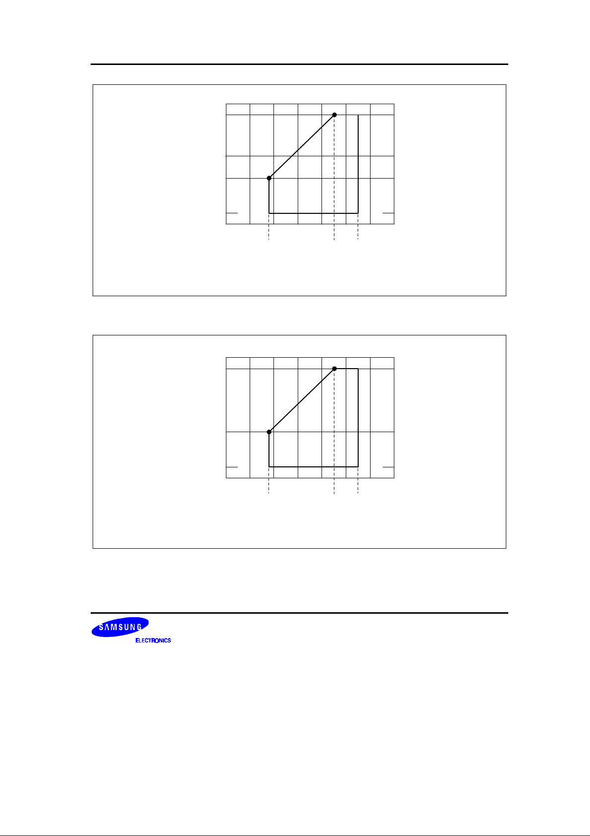
Figure 18-8. HSX Mode Operating Voltage Range
fCPU
10 MHz
B
A
3 MHZ
0.4 MHz
1 2 3 4 5 6 7
5.54.51.8
Supply Voltage (V)
Minimum instruction clock = 1/1 x oscillator frequency
Figure 18-9. MSX Mode Operating Voltage Range
18-11
Page 26
S3CB018/FB018 MECHANICAL DATA
19 MECHANICAL DATA
OVERVIEW
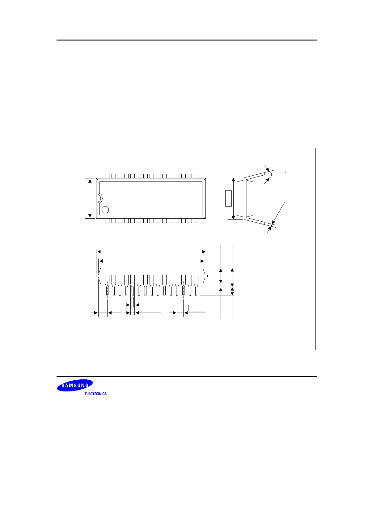
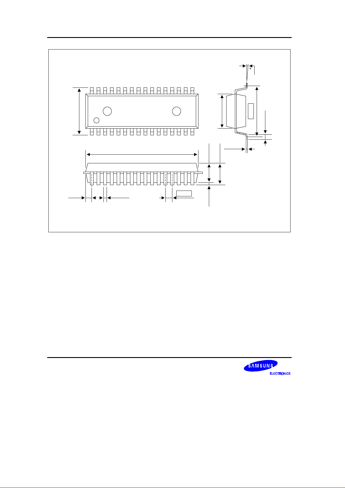
The S3CB018/FB018 is available in a 30-pin SDIP package (Samsung: 30-SDIP-400) and a 32-pin SOP package
(32-SOP-450A). Package dimensions are shown in Figures 20-1 and 20-2.
#30 #16
0.2
±
8.94
(1.30)
NOTE: Dimensions are in millimeters.
30-SDIP-400
27.88MAX
27.48
±
0.2
±
0.56
0.1
±
1.12
0.1
#15#1
1.778
10.16
0.2
±
3.81
5.08 MAX
0.3
±
3.30
0.51 MIN
0-15
+ 0.1
0.25
- 0.05
Figure 19-1. 30-Pin SDIP Package Dimensions
19-1
Page 27
MECHANICAL DATA S3CB018/FB018
0-8
#17#32
0.3
±
32-SOP-450A
12.00
#1 #16
19.90
(0.43)
NOTE: Dimensions are in millimeters
0.40
±
0.1
Figure 19-2. 32-SOP-450A Package Dimensions
0.2
0.2
11.43
8.34 ±
±
0.78
+ 0.1
0.20
0.2
±
0.2
±
2.00
- 0.05
2.40 MAX
1.27
0.05 MIN
19-2
Page 28
S3CB018/FB018 S3FB018
20 S3FB018 FLASH MCU
OVERVIEW
The S3FB018 single-chip CMOS microcontroller is the FLASH version of the S3CB018 microcontroller.
It has an on-chip FLASH ROM instead of masked ROM. The FLASH ROM is accessed in serial data format.
The S3FB018 is fully compatible with the S3CB018, both in function and in pin configuration. Because of its simple
programming requirements, the S3FB018 is ideal for use as an evaluation chip for the S3CB018.
20-1
Page 29
S3FB018 S3CB018/FB018
PIN ASSIGNMENTS
V
X
V
PP
/TEST
SI/P0.0
SO/P0.1
RESET/RESET
SCK/P0.2
BUZ/P0.3
CSI/P0.4
CSO/P0.5
CSCK/P0.6
CFSYNC/P0.7
P1.0
P1.1
P1.7
SS
XIN
1
2
3
4
5
6
7
8
9
10
11
12
13
14
15
16
S3FB018
32-SOP
(Top-View)
OUT
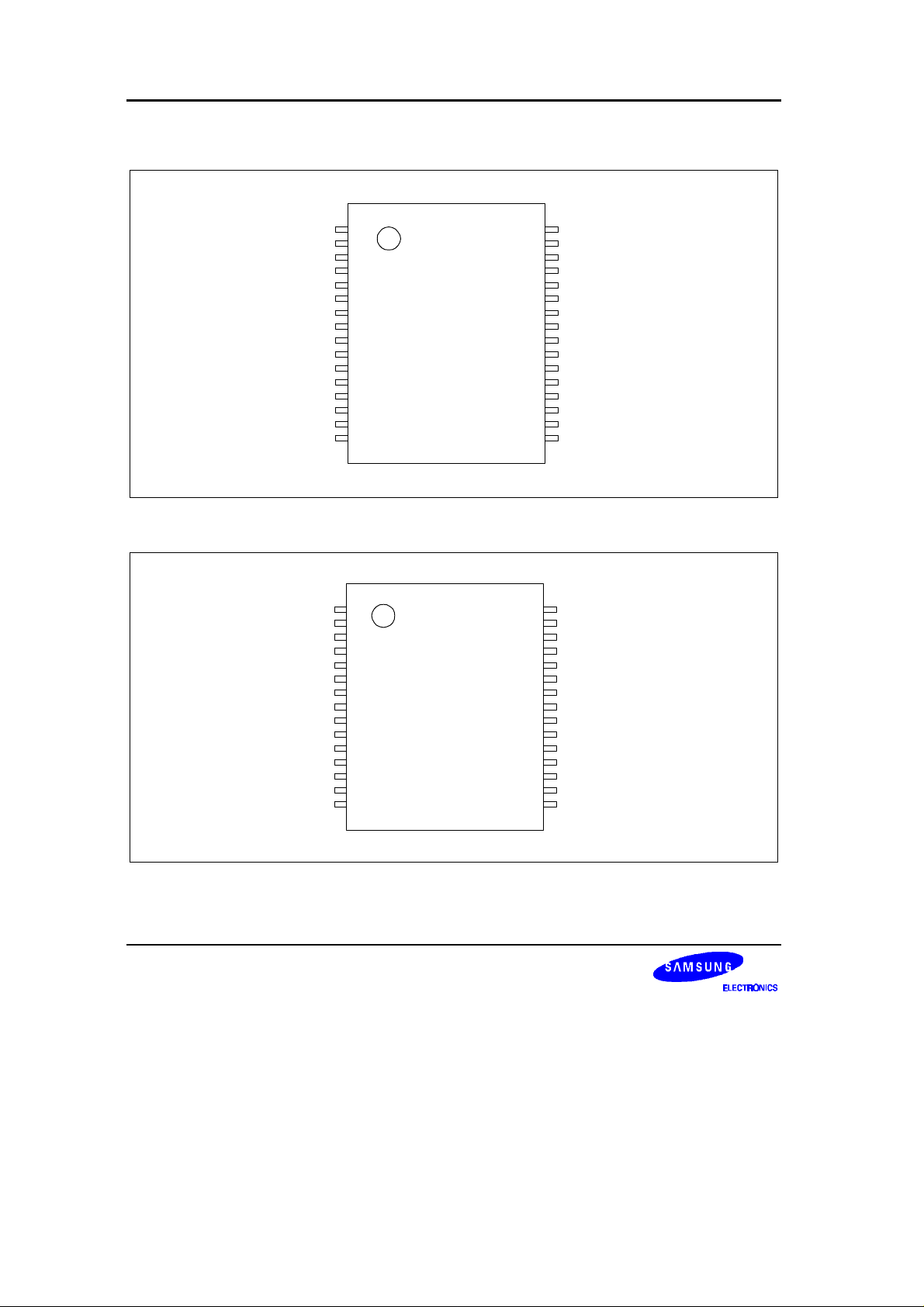
Figure 20-1. 32-SOP Pin Assignment
V
32
P3.1/INT01/
31
P3.0/INT00/SDAT
30
P2.7/TACLK
29
P2.6/TBOUT
28
P2.5/TBCLK
27
P2.4/TAOUT
26
P2.3/INT13
25
P2.2/INT12
24
P2.1/INT11
23
P2.0/INT10
22
P1.2
21
P1.3
20
P1.4
19
P1.5
18
P1.6
17
DD
SCLK
20-2
X
VPP/TEST
SI/P0.0
SO/P0.1
RESET/RESET
SCK/P0.2
BUZ/P0.3
CSI/P0.4
CSO/P0.5
CSCK/P0.6
CFSYNC/P0.7
P1.0
P1.1
XIN
1
SS
2
3
4
5
6
7
8
9
10
11
12
13
14
15
S3FB018
30-SDIP
(Top View)
V
OUT
Figure 20-2. 30-SDIP Pin Assignment
V
30
P3.1/INT01/SCLK
29
P3.0/INT00/SDAT
28
P2.7/TACLK
27
P2.6/TBOUT
26
P2.5/TBCLK
25
P2.4/TAOUT
24
P2.3/INT13
23
P2.2/INT12
22
P2.1/INT11
21
P2.0/INT10
20
P1.2
19
P1.3
18
P1.4
17
P1.5
16
DD
Page 30
S3CB018/FB018 S3FB018
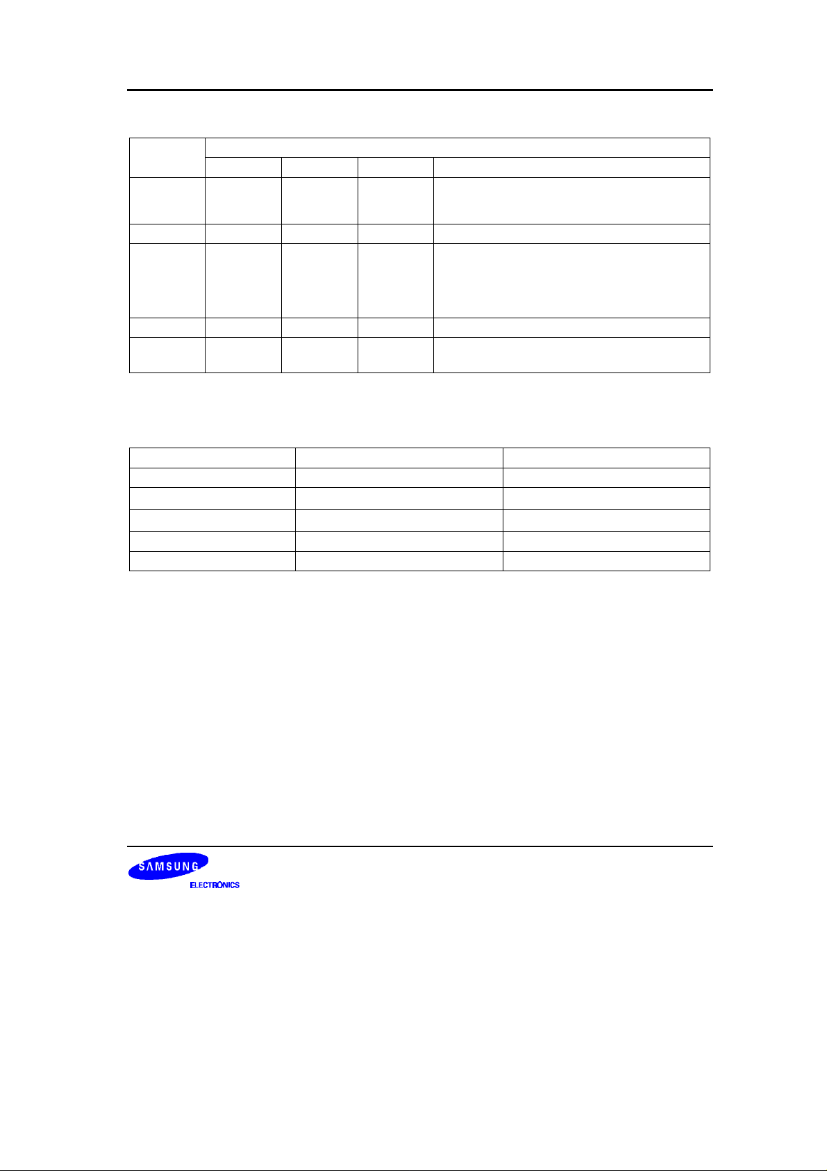
Table 20-1. Descriptions of Pins Used to Read/Write the FLASH ROM
Main Chip During Programming
Pin Name Pin Name Pin No. I/O Function
P3.0 SDAT
30(28) I/O
Serial data pin. Output port when reading and input
port when writing. Can be assigned as a Input/push-
pull output port.
P3.1 SCLK
TEST Vpp (TEST)
31(29) I/O
4 I
Serial clock pin. Input only pin.
Power supply pin for FLASH ROM cell writing
(indicates that FLASH enters into the writing mode).
When 12.5 V is applied, FLASH is in writing mode
and, when 5 V is applied, FLASH is in the reading
mode. When FLASH is operating , hold GND.
RESET RESET
VDD/V
SS
VDD/V
SS
7 I
32/1(30/1) –
Chip Initialization
Logic power supply pin. V
should be tied to
DD
+5 V during programming.
NOTE: Pin No. is for 100 QFP type package. (for 100 TQFP, the pins with the same name have same functions).
Table 20-2. Comparison of S3FB018 and S3CB018 Features
Characteristic S3FB519 S3CB519
Program Memory 4K word (8K byte) FLASH ROM 4K word (8K byte) FLASH ROM
Operating Voltage (VDD)
OTP Programming Mode
1.8 V to 5.5 V 1.8 V to 5.5 V
VDD = 5 V, V
(TEST) = 12.5 V
PP
Pin Configuration 32-SOP/30-SDIP 32-SOP/30-SDIP
FLASH ROM Programmability User programmable Programmed at the factory
20-3
Page 31
S3FB018 S3CB018/FB018
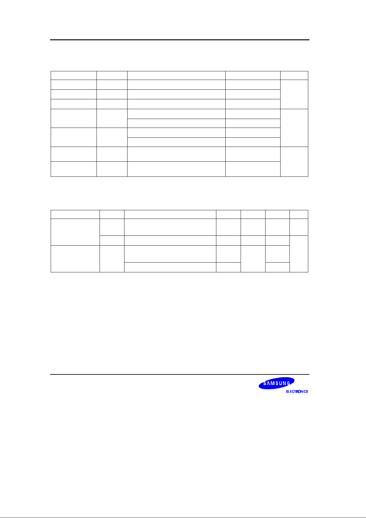
Table 20-3. Absolute Maximum Ratings
(TA = 25°C)
Parameter Symbol Conditions Rating Unit
Supply voltage
Input voltage
Output voltage
Output current
V
DD
V
I
V
O
I
OH
One I/O pin active – 18 mA
– – 0.3 to + 6.0 V
–
–
– 0.3 to V
– 0.3 to VDD + 0.3
DD
+ 0.3
high All I/O pins active – 60
Output current
I
OL
One I/O pin active + 30
low Total pin current for ports 1, 2, 3 + 100
Operating
temperature
Storage
temperature
T
T
A
STG
– – 40 to + 85
– – 65 to + 150
°
C
Table 20-4. D.C. Electrical Characteristics
(T
= – 40°C to + 85°C, VDD = 1.8 V to 5.5 V)
A
Parameter Symbol Conditions Min Typ Max Unit
Operating Voltage
V
DD
F
CPU
= 20 MHz
4.5 – 5.5 V
(HSX mode)
F
Operating Voltage
= 3 MHz
CPU
V
DD
F
CPU
= 10 MHz
1.8 5.5
4.5 – 5.5
(MSX mode)
F
CPU
= 3 MHz
1.8 5.5
20-4
Page 32
S3CB018/FB018 S3FB018
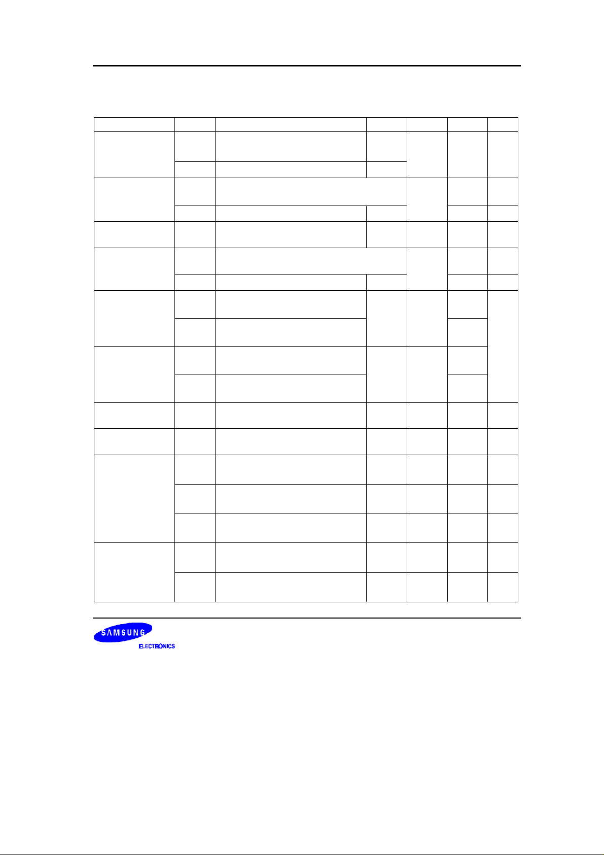
Table 20-4. D.C. Electrical Characteristics (Continued)
(T
= – 40°C to + 85°C, VDD = 1.8 V to 5.5 V)
A
Parameter Symbol Conditions Min Typ Max Unit
Input high voltage
V
All input pins except V
IH1
IH2
0.8 V
DD
–
V
DD
V
Input low voltage
Output high voltage
Output low voltage
Input high leakage
current
Input low leakage
current
Output high leakage
current
Output low leakage
current
Oscillator feed back
resistors
Pull-up resistor
V
IH2
V
IL1
V
IL2
V
OH1VDD
V
OL1VDD
V
OL2VDD
I
LIH1
I
LIH2
I
LIL1
I
LIL2
I
LOH
I
LOL
R
osc1
(HSX)
R
osc2
(MSX)
R
osc3
(LSX)
R
L1
R
L2
X
IN
All input pins except V
X
IN
IL2
= 5V; IOH = -1 mA
All output pins
= 5V; IOL = 8 mA
All output pins except V
OL2
= 5V; IOL = 15 mA, Port 1
VIN = V
DD
All input pins except I
VIN = V
DD
XIN, XT
IN
V
= 0 V
IN
All input pins except I
LIH2
LIL2
VIN = 0 V
XIN, XTIN, RESET
V
= V
OUT
DD
All I/O pins and Output pins
V
= 0 V
OUT
All I/O pins and Output pins
VDD = 5.0 V, TA = 25°C
XIN = VDD, X
OUT
= 0V
VDD = 5.0 V, TA = 25°C
XIN = VDD, X
OUT
= 0V
VDD = 5.0 V, TA = 25°C
XIN = VDD, X
OUT
= 0V
VIN = 0 V; VDD = 5 V ± 10%
Ports 0,1,2,3,4,5 TA=25°C
VIN = 0 V; V
= 5 V ± 10%
DD
TA=25°C, RESET only
V
0.1
-
DD
– –
0.2 V
DD
0.1
VDD-1.0
– – V
– – 2
2
– – 3 uA
20
– – -3
-20
– – 3 uA
– – -3
510 710 910
510 710 910
2.0 2.7 3.5
30 50 70
110 210 310
kΩ
MΩ
kΩ
20-5
Page 33
S3FB018 S3CB018/FB018
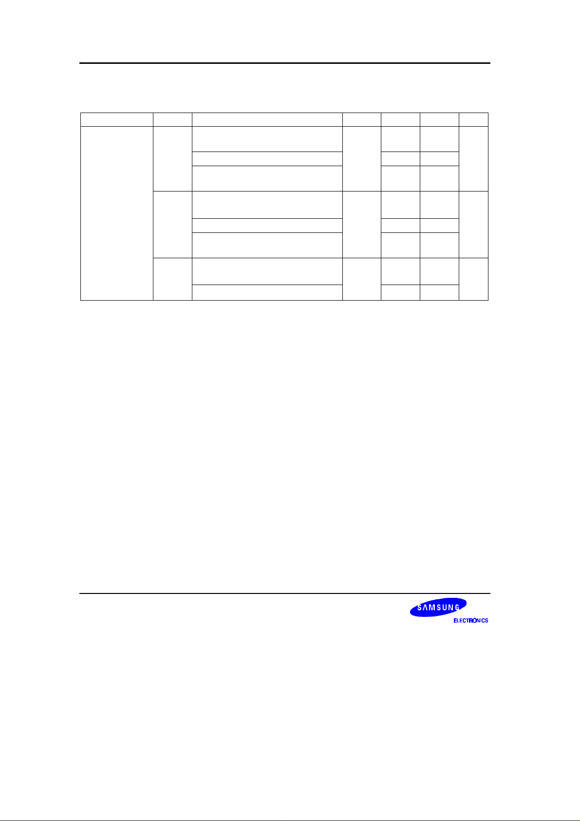
Table 20-4. D.C. Electrical Characteristics (Continued)
(T
= – 40°C to + 85°C, VDD = 1.8 V to 5.5 V)
A
Parameter Symbol Conditions Min Typ Max Unit
Supply current
(1)
I
DD1
(2)
Operating mode: V
= 5 V ± 10%
DD
– 10 20 mA
20 MHz crystal oscillator(HSX)
5 MHz crystal oscillator(MSX)
V
= 3 V ± 10%
DD
4 8
2 4
5 MHz crystal oscillator(MSX)
(3)
I
DD2
Idle mode: VDD = 5 V ± 10%
– 2.5 5 mA
20 MHz crystal oscillator(HSX)
5 MHz crystal oscillator(MSX)
VDD = 3 V± 10%
1 2
0.4 0.8
5 MHz crystal oscillator(MSX)
I
NOTES:
1. Supply current does not include current drawn through internal pull-up resistors or external output current loads.
2. In operating current test mode Timer A and Timer B are running.
3. In idle current test mode the Watch timer is running.
4. The operating and idle currents are measured at weak mode.
DD3
Stop mode
V
= 5 V ± 10%
DD
V
= 3 V ± 10%
DD
– 0.5 3 uA
0.2 1.2
20-6
 Loading...