

Page 1

S3C8835/C8837/P8837 PRODUCT OVERVIEW
1 PRODUCT OVERVIEW
SAM87 PRODUCT FAMILY
Samsung's SAM87 family of 8-bit single-chip CMOS microcontrollers offers a fast and efficient CPU, a wide
range of integrated peripherals, and various mask-programmable ROM sizes. Important CPU features include:
— Efficient register-oriented architecture
— Selectable CPU clock sources
— Release by interrupt of Idle and Stop power-down modes
— Built-in basic timer circuit with watchdog function
A sophisticated interrupt structure recognizes up to eight interrupt levels. Each level can have one or more
interrupt sources and vectors. Fast interrupt processing (within a minimum six CPU clocks) can be assigned to
specific interrupt levels.
S3C8835/C8837/P8837
The S3C8835 microcontroller has 16 K bytes of on-chip program memory and the S3C8837 has 24 K bytes. Both
chips have a 272-byte general-purpose internal register file. The interrupt structure has seven interrupt sources
with six interrupt vectors. The CPU recognizes six interrupt priority levels.
Using a modular design approach, the following peripherals were integrated with the SAM87 core to make the
S3C8835/C8837/P8837 suitable for use in color television and other types of screen display applications:
— Four programmable I/O ports (26 pins total: 16 general-purpose I/O pins; 8 n-channel, open-drain output pins)
— 2 channel A/D converter (4-bit resolution)
— 14-bit PWM output (one channels: push-pull type)
— Basic timer (BT) with watchdog timer function
— One 8-bit timer/counter (T0) with interval timer
— One 8-bit general-purpose timer/counter (TA) with prescalers
— On-screen display (OSD) with a wide range of programmable features including halftone control signal output
The S3C8835/C8837 are available in a versatile 42-pin SDIP package.
OTP
The S3C8835/C8837 microcontroller is also available in OTP (One Time Programmable) version, S3P8837.
S3P8837 microcontroller has an on-chip 24K-byte one-time-programmable EPROM instead of masked ROM.
The S3P8837 is comparable to S3C8835/C8837, both in function and in pin configuration.
1-1
Page 2

PRODUCT OVERVIEW S3C8835/C8837/P8837
FEATURES
CPU
• SAM87 CPU core
Memory
• 16-K byte (S3C8835) or 24K- byte (S3C8837)
internal program memory
• 272-byte general-purpose register area
Instruction Set
• 78 instructions
• IDLE and STOP instructions added for powerdown modes
Instruction Execution Time
• 750 ns (minimum) with an 8-MHz CPU clock
Interrupts
• 7 interrupt sources with 6 vectors
• 6 interrupt levels
• Fast interrupt processing for select levels
General I/O
Pulse Width Modulation Module
• 14-bit PWM with one-channel output (push-pull
type)
• PWM counter and data capture input pin
• Frequency: 5.859 kHz to 23.437 kHz with a
6-MHz CPU clock
On-Screen Display (OSD)
• Video RAM: 252 × 12 bits
• Character generator ROM: 256 × 18 × 16 bits
(256 display characters: fixed: 2, variable: 254)
• 252 display positions (12 rows × 21 columns)
• 16-dot × 18-dot character resolution
• 16 different character sizes
• Eight character colors
• Vertical direction fade-in/fade-out control
• Eight colors for character and frame background
• Halftone control signal output; selectable for
individual characters
• Synchronous polarity selector for H-sync and
V-sync input
• Four I/O ports (26 pins total)
• Six open-drain pins for up to 6-volt loads
• Two open-drain pins for up to 5-volt loads
8-Bit Basic Timer
• Three selectable internal clock frequencies
• Watchdog or oscillation stabilization function
Timer/Counters
• One 8-bit timer/counter (T0) with three internal
clocks and interval timer mode.
• One general-purpose 8-bit timer/counters with
interval timer mode (timer A)
A/D Converter
• Two analog input pins; 4-bit resolution
• 3.125 µs conversion time (8-MHz CPU clock)
Oscillator Frequency
• 5-MHz to 8-MHz external crystal oscillator
• Maximum 8-MHz CPU clock
Operating Temperature Range
• – 20°C to + 85°C
Operating Voltage Range
• 4.5 V to 5.5 V
Package Type
• 42-pin SDIP
1-2
Page 3
S3C8835/C8837/P8837 PRODUCT OVERVIEW
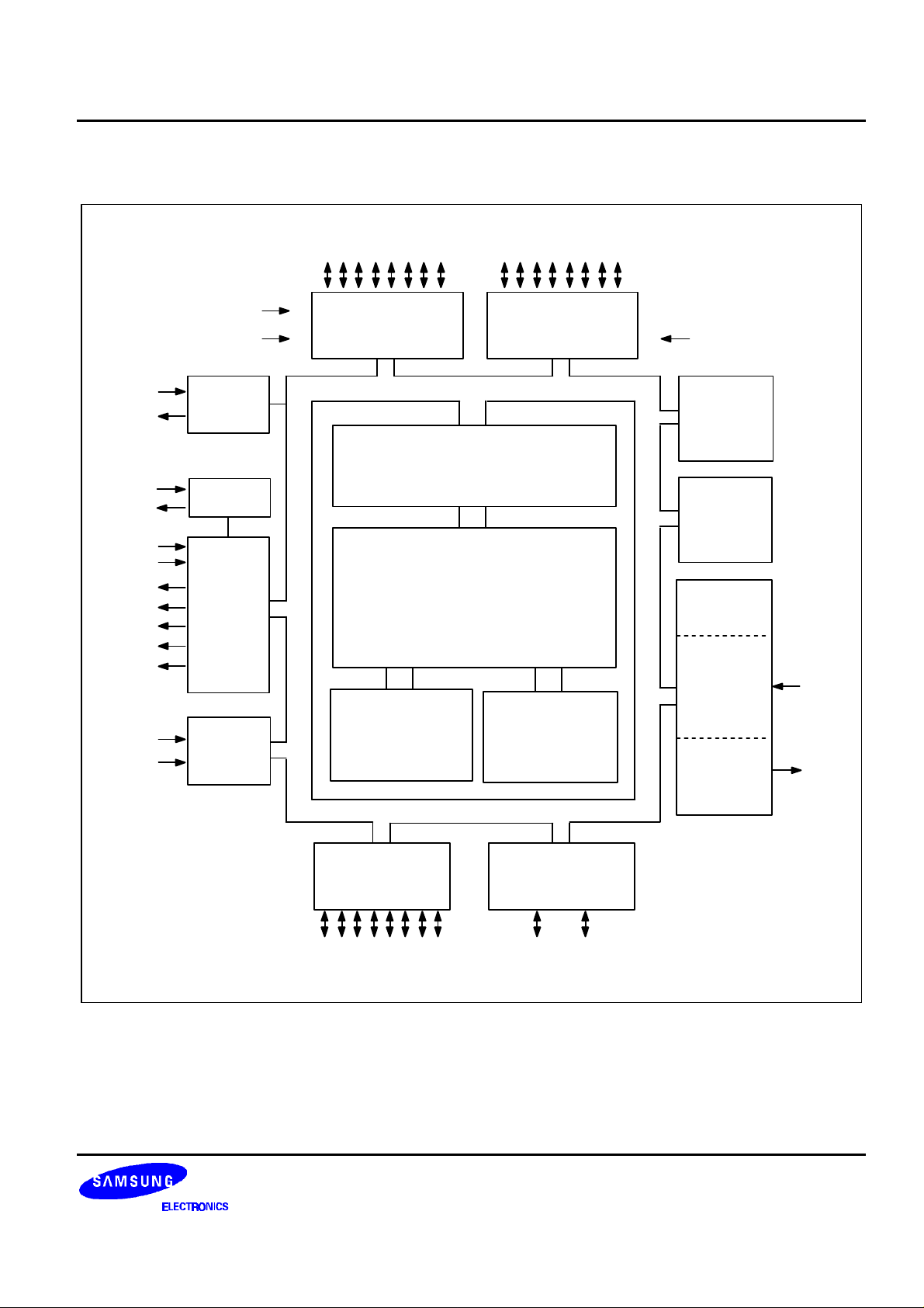
BLOCK DIAGRAM
X
OSC
OSC
H-sync
V-sync
Vgreen
Vblue
Vblank
OSDHT
ADC0
ADC1
X
IN
OUT
IN
OUT
Vred
RESET
INT0 - INT1
MAIN
OSC
L-C OSC
ON-
SCREEN
DISPLAY
4-BIT
ADC
P0.0 - P0.7
PORT 0 PORT 1
SAM87 BUS
PORT I/O and INTERRUPT
CONTROL
SAM87 CPU
16KB ROM (8835)
24KB ROM (8837)
SAM87 BUS
P1.0 - P1.7
272-BYTE
REGISTER FILE
TEST
TIMER A
TIMER 0
PWM
BLOCK
PWM
COUNTER
and DATA
CAPTURE
14-BIT
PWM
CAPA
PWM0
PORT 2
P2.0 - P2.7
Figure 1-1. Block Diagram
PORT 3
P3.0 - P3.1
1-3
Page 4

PRODUCT OVERVIEW S3C8835/C8837/P8837
PIN ASSIGNMENTS
P2.5/PWM0
P2.1
P2.2(
SCL
P2.3(
SDA
P2.4
P2.0
P2.6
P1.7
P3.0/ADC0
P3.1/ADC1
P0.6
P0.7
TEST
P1.0/INT0
P1.1/INT1
P1.2
P1.3
P1.4
P1.5
P1.6
P2.7/OSDHT
1
2
)
3
)
4
5
6
7
8
9
10
11
12
13
S3C8835
S3C8837
42-PIN SDIP
(Top View)
14
15
16
17
18
19
20
21
42
41
40
39
38
37
36
35
34
33
32
31
30
29
28
27
26
25
24
23
22
P0.0
P0.1
P0.2
P0.3
P0.4
V
SS2
CAPA
P0.5
V
DD
RESET
X
OUT
X
IN
V
SS1
OSC
OUT
OSC
IN
V-sync
H-sync
Vblank
Vred
Vgreen
Vblue
1-4
Figure 1-2. S3C8835/C8837/P8837 Pin Assignment Diagram
Page 5

S3C8835/C8837/P8837 PRODUCT OVERVIEW
Table 1-1. S3C8835/C8837 Pin Descriptions
Pin Name Pin
Pin Description Circuit
Type
P0.0–P0.7 I/O General I/O port (8-bit), configurable for
digital input or push-pull output.
P1.0–P1.1 I/O General I/O port (2-bit), configurable for
digital input or n-channel open-drain output.
P1.0–P1.1 can withstand up to 6-volt loads.
Multiplexed for alternative use as external
interrupt inputs INT0–INT1.
P1.2–P1.5 General I/O port (4-bit), configurable for
digital input or n-channel open-drain output.
P1.2–P1.5 can withstand up to 6-volt loads.
High current port (10mA).
P1.6–P1.7 General I/O port (2-bit), configurable for
digital input or push-pull output.
P2.0–P2.4,
P2.6
I/O General I/O port (6-bit). I/O mode or
n-channel open-drain, push-pull output
mode is software configurable. Pins can
withstand up to 5-volt loads.
P2.2: OTP serial clock pin
P2.3: OTP serial data pin
P2.5, P2.7 General I/O port (2-bit). I/O mode or
n-channel open-drain, push-pull output
mode is software configurable. Pins can
withstand up to 5-volt loads.
Each pin has an alternative function.
P2.5: PWM0 (14-bit PWM output)
P2.7: OSDHT (Halftone signal output)
Type
Pin
Numbers
Share
Pins
3 11–12, 35,
38–42
7 14–15 INT0–INT1
5 16–19
3 20, 8
2 2–7
2 1, 21 PWM0
OSDHT
1-5
Page 6
PRODUCT OVERVIEW S3C8835/C8837/P8837
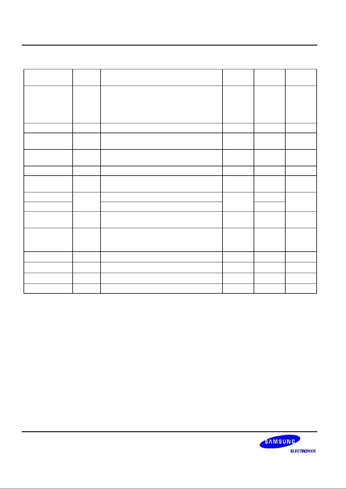
Table 1-1. S3C8835/C8837 Pin Descriptions (Continued)
Pin Name Pin
Type
P3.0–P3.1 I/O General I/O port (2 bits), configurable for
digital input or n-channel open-drain output.
Pin Description Circuit
Type
6 9–10 ADC0
Pin
Numbers
Share
Pins
ADC1
P3.0–P3.1 can withstand up to 5-volt loads.
Multiplexed for alternative use as external
interrupt inputs ADC0–ADC1.
PWM0 O Output pin for 14-bit PWM0 circuit 2 1 P2.5
ADC0–ADC1 I Analog inputs for 4-bit A/D converter 6 9,10 P3.0–
P3.1
INT0–INT1 I External interrupt input pins 7 14,15 P1.0–
P1.1
OSDHT O Halftone control signal output for OSD 2 21 P2.7
Vblue, Vgreen
Vred, Vblank
O Digital blue, green, red, and video blank
signal outputs for OSD
4 22–25 –
H-sync I H-sync input for OSD 8 26 –
V-sync V-sync input for OSD 27
OSC
IN,
OSC
OUT
I, O L-C oscillator pins for OSD clock frequency
– 28,29 –
generation
TEST I
0 V: Normal operation mode
– 13 –
5 V: Factory test mode
12.5 V: OTP write mode
X
IN, XOUT
RESET
V
DD, VSS1, VSS2
I, O System clock pins – 31, 32 –
I System reset input pin 1 33 –
– Power supply pins – 13 –
CAPA I Input for capture A module 8 26 –
1-6
Page 7

S3C8835/C8837/P8837 PRODUCT OVERVIEW
PIN CIRCUITS
V
DD
V
DD
DATA I/O
200 K
Ω
NOISE
FILTER
Figure 1-3. Pin Circuit Type 1 (RESETRESET)
V
DD
DATA
OPENDRAIN
OUTPUT
DISABLE
INPUT
V
SS
INPUTIN
V
SS
INPUT
Figure 1-5. Pin Circuit Type 3
(P0.0–P0.7, P1.6–P1.7)
V
DD
I/O
DATA I/O
V
SS
Figure 1-4. Pin Circuit Type 2
(P2.0–P2.7, PWM0, OSDHT)
Figure 1-6. Pin Circuit Type 4
(Vblue, Vgreen, Vred, Vblank)
1-7
Page 8

PRODUCT OVERVIEW S3C8835/C8837/P8837
I/O
I/O
DATA
DATA
V
SS
V
SS
INPUT
INPUT
INT
NOISE FILTER
NOTE:
Circuit type 5 can withstand up to
6-volt loads.
Figure 1-7. Pin Circuit Type 5 (P1.2–P1.5)
I/O
DATA
V
SS
INPUT
A/D IN
NOTE:
Circuit type 7 can withstand up to
6-volt loads.
Figure 1-9. Pin Circuit Type 7
(P1.0–P1.1, INT0–INT1)
INPUT IN
NOISE
FILTER
1-8
NOTE:
Circuit type 6 can withstand up to
5-volt loads.
Figure 1-8. Pin Circuit Type 6
(P3.0–P3.1, ADC0–ADC1)
Figure 1-10. Pin Circuit Type 8
(V-Sync H-Sync, CAPA)
Page 9

S3C8835/C8837/P8837 ELECTRICAL DATA
15 ELECTRICAL DATA
OVERVIEW
In this section, S3C8835/C8837 electrical characteristics are presented in tables and graphs. The information is
arranged in the following order:
— Absolute maximum ratings
— D.C. electrical characteristics
— I/O capacitance
— A.C. electrical characteristics
— Input timing measurement points for t
NF1
and t
NF2
— Data retention supply voltage in Stop mode
— Stop mode release timing when initiated by RESET
— Main oscillator and L-C oscillator frequency
— Clock timing measurement points for X
— Main oscillator clock stabilization time (tST)
— A/D converter electrical characteristics
— Characteristic curves
IN
15-1
Page 10

ELECTRICAL DATA S3C8835/C8837/P8837
Table 15-1. Absolute Maximum Ratings
(TA = 25°C)
Parameter Symbol Conditions Rating Unit
Supply Voltage
Input Voltage
Output Voltage
Output Current
V
DD
I
V
V
V
I1
I2
O
OH
P1.0–P1.5 (open-drain) – 0.3 to + 7 V
All port pins except V
All output pins
One I/O pin active – 18 mA
– – 0.3 to + 6.0 V
I1
– 0.3 to VDD + 0.3
– 0.3 to VDD + 0.3
V
High
All I/O pins active – 60
Output Current
I
OL
One I/O pin active + 30 mA
Low
Total pin current for port 1 + 100
Total pin current for ports 0, 2, and 3 + 100
Operating
T
A
– – 20 to + 85
°
C
Temperature
Storage
T
STG
– – 65 to + 150
°
C
Temperature
Table 15-2. D.C. Electrical Characteristics
(T
= – 20°C to + 85°C, VDD = 4.5 V to 5.5 V)
A
Parameter Symbol Conditions Min Typ Max Unit
Input High
V
IH1
All input pins except V
IH2
0.8 V
DD
–
V
DD
Voltage
X
X
IN,
OUT
All input pins except V
X
X
IN,
OUT
IOH = – 500 µA
P0, P1.6–P1.7, P2
IL2
2.7 V
– –
V
– 0.8
DD
0.2 V
DD
1.0 V
– – V
Input Low Voltage
Output High
Voltage
V
IH2
V
IL1
V
IL2
V
OH
R, G, B, Vblank
Output Low
Voltage
V
OL1
V
OL2
IOL = 4 mA
P0, P1.6–P1.7
IOL = 10 mA
– – 0.4 V
– – 0.8
P1.2–P1.5
V
OL3
IOL = 2 mA
– – 0.4
P1.0–P1.1, P3.0–P3.1
V
OL4
IOL = 1 mA
– – 0.4 V
R, G, B, Vblank, P2
V
V
15-2
Page 11
S3C8835/C8837/P8837 ELECTRICAL DATA
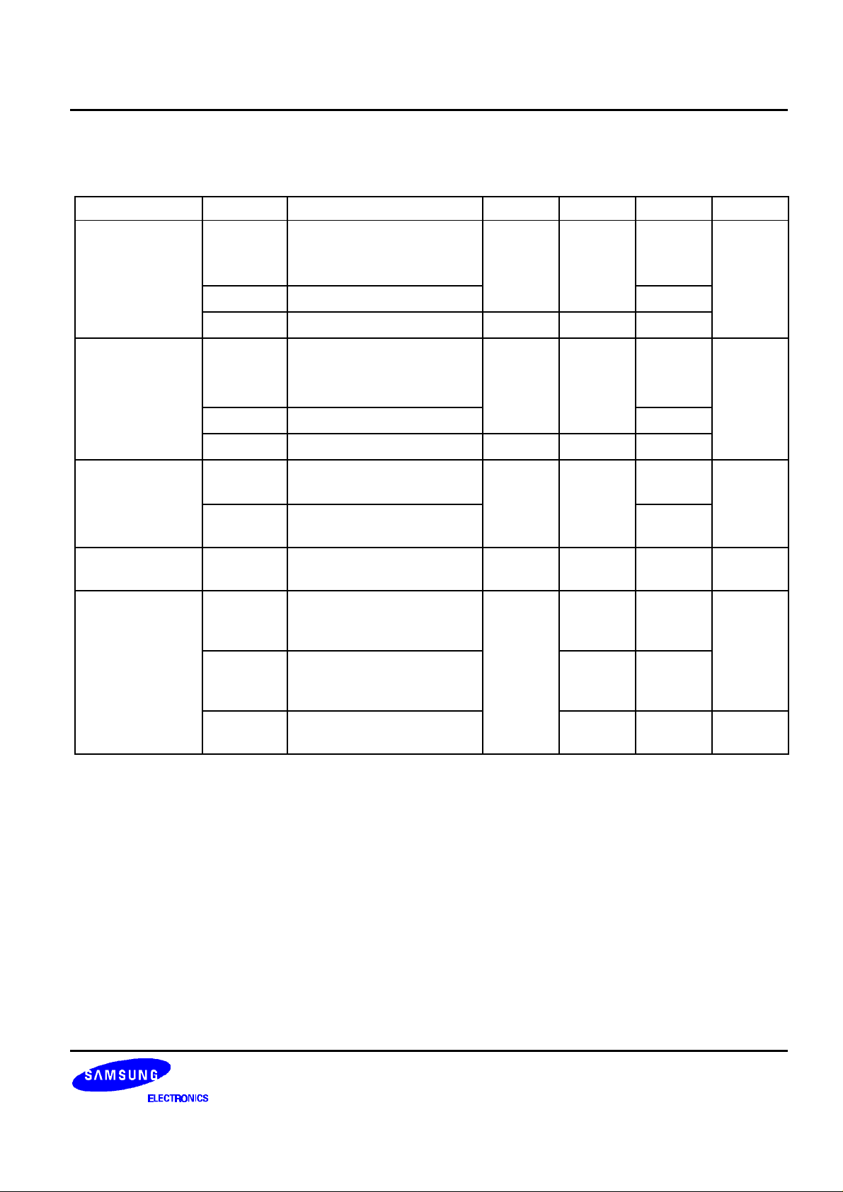
Table 15-2. D.C. Electrical Characteristics (Continued)
(TA = – 20°C to + 85°C, VDD = 4.5 V to 5.5 V)
Parameter Symbol Conditions Min Typ Max Unit
Input High
Leakage Current
Input Low
Leakage Current
Output High
Leakage Current
I
LIH1
I
LIH2
I
LIH3
I
LIL1
I
LIL2
I
LIL3
I
LOH1
I
LOH2
VIN = V
DD
All input pins except I
and I
LIH3
VIN = V
VIN = V
V
= 0 V
IN
OSC
DD,
DD, XIN,
IN,
X
OSC
OUT
All input pins except I
I
and RESET
LIL3,
V
= 0 V, OSC
IN
V
= 0 V, X
IN
V
= V
OUT
DD
IN,
IN,
X
OSC
OUT
All output pins except I
V
= 6 V
OUT
LIH2
LIL2,
OUT
LOH2
OUT
– – 3 µA
10
2.5 10 20
– – – 3 µA
– 10
– 2.5 – 10 – 20
– – 3 µA
10
P1.0–P1.5
Output Low
Leakage Current
Supply Current
(note)
I
LOL
I
DD1
V
= 0 V
OUT
All output pins
Normal mode;
V
= 4.5 V to 5.5 V
DD
– – – 3 µA
– 7 20 mA
8-MHz CPU clock
I
DD2
Idle mode;
V
= 4.5 V to 5.5 V
DD
2 10
8-MHz CPU clock
I
DD3
Stop mode;
V
= 4.5 V to 5.5 V
DD
1 10 µA
NOTE: Supply current does not include current drawn through internal pull-up resistors or external output current loads.
15-3
Page 12

ELECTRICAL DATA S3C8835/C8837/P8837
Table 15-3. Input/Output Capacitance
(T
= – 20°C to + 85°C, V
A
DD
= 0 V)
Parameter Symbol Conditions Min Typ Max Unit
C
C
OUT
IN
f = 1 MHz; unmeasured pins
are connected to V
SS
– – 10 pF
Input
capacitance
Output
capacitance
I/O capacitance
C
IO
Table 15-4. A.C. Electrical Characteristics
(T
= – 20°C to + 85°C, V
A
= 4.5 V to 5.5 V)
DD
Parameter Symbol Conditions Min Typ Max Unit
V-sync Pulse
t
VW
– 4 – – µs
Width
H-sync Pulse
t
HW
– 3 – – µs
Width
Noise Filter
t
NF1
t
NF2
t
NF3
t
NF4
t
NF5
P1.0–P1.1, V-sync – 350 – ns
RESET
– 1000
Glitch filter (oscillator block) – 15
CAPA – 5 –
t
CAPA
H-sync – 650 – ns
NOTE: t
CAPA
= f
/128.
OSC
1t
CPU
t
NF1L
t
NF2
0.8 V
0.2 V
Figure 15-1. Input Timing Measurement Points for t
DD
DD
t
NF1H
NF1
and t
NF2
15-4
Page 13

S3C8835/C8837/P8837 ELECTRICAL DATA
Table 15-5. Data Retention Supply Voltage in Stop Mode
(TA = – 20 °C to + 85 °C)
Parameter Symbol Conditions Min Typ Max Unit
Data Retention
V
DDDR
Stop mode 2 – 6 V
Supply Voltage
Data Retention
I
DDDR
Stop mode, V
DDDR
= 2.0 V
– – 5 µA
Supply Current
NOTES:
1. Supply current does not include current drawn through internal pull-up resistors or external output current loads.
2. During the oscillator stabilization wait time (t
~
~
~
~
V
DD
EXECUTION OF
STOP INSTRUCTION
RESET
), all CPU operations must be stopped.
WAIT
STOP MODE
DATA RETENTION MODE
V
DDDR
t
SREL
OSCILLATION
STABILIZATION
TIME
NORMAL
OPERATING
MODE
NOTE:
t
is the same as 4096 x 16 x 1 / f
WAIT
OSC
t
WAIT
Figure 15-2. Stop Mode Release Timing When Initiated by a Reset
15-5
Page 14

ELECTRICAL DATA S3C8835/C8837/P8837
Table 15-6. Main Oscillator and L-C Oscillator Frequency
(TA = – 20°C to + 85°C, VDD = 4.5 V to 5.5 V)
Oscillator Clock Circuit Conditions Min Typ Max Unit
Crystal
C1
C2
X
X
IN
OSD block active 5 6 8 MHz
OUT
OSD block inactive 0.5 6 8
Ceramic
C1
C2
X
X
IN
OSD block active 5 6 8 MHz
OUT
OSD block inactive 0.5 6 8
External Clock
X
IN
OSD block active 5 6 8 MHz
X
OUT
OSD block inactive 0.5 6 8
L-C Oscillator
C1
C2
OSC
OSC
Recommend value:
IN
C1 = C2 = 20 pF
OUT
5 6.5 8 MHz
CPU Clock Frequency – 0.032 6.0 8 MHz
1 / f
OSC
t
XL
X
IN
t
XH
2.7 V
1.0 V
15-6
Figure 15-3. Clock Timing Measurement Points for X
IN
Page 15

S3C8835/C8837/P8837 ELECTRICAL DATA
Table 15-7. Main Oscillator Clock Stabilization Time
(TA = – 20°C to + 85°C, VDD = 4.5 V to 5.5 V)
Oscillator Symbol Test Condition Min Typ Max Unit
Crystal –
VDD = 4.5 V to 6.0 V
– – 20 ms
Ceramic (Oscillation stabilization occurs when
10
VDD is equal to the minimum oscillator
voltage range.)
External Clock
Release Signal
t
SREL
XIN input High and Low level width
(t
XH, tXL
)
65 – 100 ns
Normal operation – 1000 – ns
Setup Time
Oscillation
Stabilization
Wait Time
(1)
t
WAIT
CPU clock = 8 MHz; Stop mode
released by RESET
CPU clock = 8 MHz; Stop mode
– 8.3 – ms
(2)
released by an interrupt
NOTES:
1. Oscillation stabilization time is the time required for the CPU clock to return to its normal oscillation frequency after a
power-on occurs, or when Stop mode is released.
2. The oscillation stabilization interval is determined by the basic timer (BT) input clock setting.
Table 15-8. A/D Converter Electrical Characteristics
(T
= – 20°C to + 85°C, VDD = 4.5 V to 5.5 V, VSS = 0 V)
A
Parameter Symbol Conditions Min Typ Max Unit
Absolute
Accuracy
(1)
Conversion
(2)
Time
Analog Input
– CPU clock = 8 MHz – –
t
CON
V
IAN
–
t
CPU
(3)
V
SS
× 25
± 0.5
LSB
– µs
–
V
DD
V
Voltage
Analog Input
R
AN
– 2 –
MΩ
Impedance
NOTES:
1. Excluding quantization error, absolute accuracy values are within ± 1/2 LSB.
2. 'Conversion time' is the time required from the moment a conversion operation starts until it ends.
3. The unit t
means one CPU clock period.
CPU
15-7
Page 16

S3C8835/C8837/P8837 MECHANICAL DATA
16 MECHANICAL DATA
OVERVIEW
The S3C8835/C8837 microcontrollers are available in a 42-pin SIP package (42-SDIP-600).
14.00 ± 0.2
(1.77)
0.50 ± 0.1
42 22
42-SDIP-600
#1 21
39.10 ± 0.2
1.00 ± 0.1
1.778
15.24
0.51MIN 3.50 ± 0.2
3.30 ± 0.3 5.08MAX
+0.1
– 0.05
0.25
0 ~ 15 °
: Package dimensions are in millimeters.
NOTE
Figure 16-1. 42-Pin SDIP Package Mechanical Data (42-SDIP-600)
16-1
Page 17

S3C8835/C8837/P8837 S3P8837 OTP
17 S3P8837 OTP
OVERVIEW
The S3P8837 single-chip CMOS microcontroller is the OTP (One Time Programmable) version of the
S3C8835/C8837 microcontroller. It has an on-chip OTP ROM instead of masked ROM. The EPROM is accessed
by serial data format.
The S3P8837 is fully compatible with the S3C8835/C8837, both in function and in pin configuration. Because of
its simple programming requirements, the S3P8837 is ideal for use as an evaluation chip for the
S3C8835/C8837.
17-1
Page 18
S3P8837 OTP S3C8835/C8837/P8837
P2.7 /OSDHT
P0.7
P0.6
P0.5
P0.4
P0.3
P0.2
P0.1
P0.0
/VSS
VSS
/VDD
VDD
X
OUT
X
IN
P2.6
RESETRESET /RESET
P2.5/PWM0
P2.4
/P2.3
SDA
/P2.2
SCL
P2.1
P2.0
1
2
3
4
5
6
7
8
9
10
11
12
13
14
15
16
17
18
19
20
21
S3P8837
42-PIN SDIP
(Top View)
42
41
40
39
38
37
36
35
34
33
32
31
30
29
28
27
26
25
24
23
22
OSC
OUT
OSC
IN
Vblank
Vblue
Vgreen
Vred
V-sync
H-sync
P1.0/INT0
P1.1/INT1
P1.2
P1.3
P1.4
P1.5
P1.6
TEST/
TEST
CAP.A
VSS/
VSS
P1.7
P3.0/ADC0
P3.1/ADC1
NOTE:
The bolds indicate an OTP pin name.
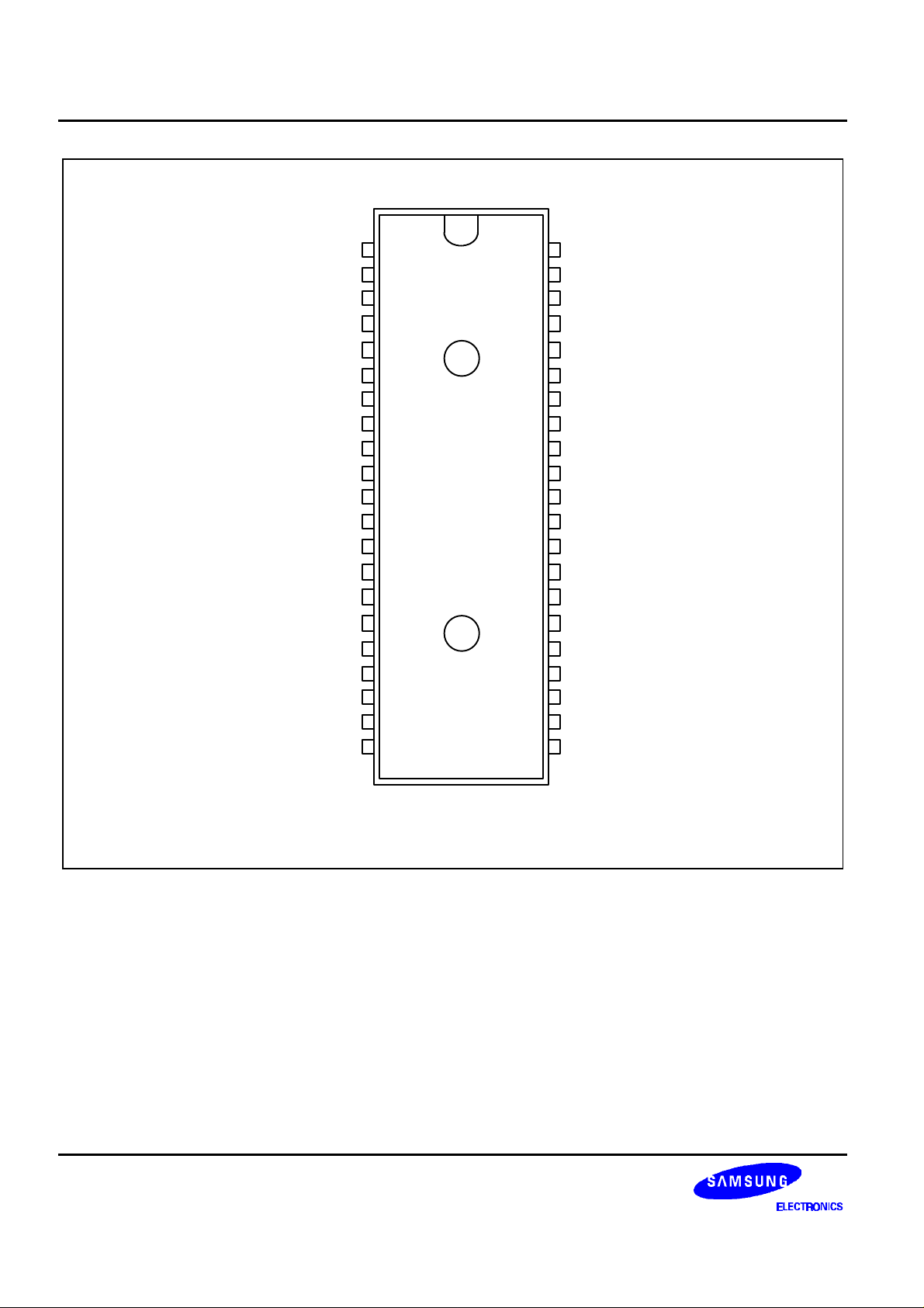
Figure 17-1. S3P8837 Pin Assignments (42-SDIP)
17-2
Page 19

S3C8835/C8837/P8837 S3P8837 OTP
Table 17-1. Descriptions of Pins Used to Read/Write the EPROM
Main Chip During Programming
Pin Name Pin Name Pin No. I/O Function
P2.3 (Pin 4) SDAT 4 I/O Serial data Pin (Output when reading, Input
when writing) Input and Push-pull Output Port
can be assigned
P2.2 (Pin 3) SCLK 3 I/O Serial clock Pin (Input Only Pin)
V
TEST
PP
(TEST)
13 I 0 V: Operating mode
5 V: Test mode
12.5 V: OTP mode
RESET RESET
33 I 0 V: Chip initialization, OTP mode
5 V: Operating mode
VDD/V
SS
VDD/V
SS
34/30, 37 I Logic Power Supply Pin.
Table 17-2. Comparison of S3P8837 and S3C8835/C8837 Features
Characteristic S3P8837 S3C8835/C8837
Program Memory 24K-byte EPROM 24K-byte mask ROM
Operating Voltage (VDD)
4.5 V to 5.5 V 4.5 V to 5.5 V
OTP Programming Mode
VDD = 5 V, V
(TEST) = 12.5 V
PP
–
Pin Configuration 42-SDIP 42-SDIP
EPROM Programmability User Program 1 time Programmed at the factory
17-3
 Loading...