

Page 1
SUMMIT
MICROELECTRONICS, Inc.
Hot Swap Voltage Controller
S39421
FEATURES
• Full Voltage Control for Hot Swap Applications
– Card Insertion Detection
– Platform Voltage Detection
– Card Voltage Sequencing
– 5 Volt, 12 Volt and 3.3 Volt
• 12 Volt FET Enable Outputs
– Allows use of Low On-resistance N-Channel
FETS
• Card Reset Generation Based on Out of Spec
Voltages
– Host Reset
• Programmable Slew Rate Control [250V/Sec
Default Rate]
• Supports 5 Volt, 3.3 Volt and Mixed Voltage
Cards
• Integrated 1K Bit E
2
PROM Memory
• Data Download™ Mode [Simplifies
Downloading of Configuration Memory into
Interface ASIC or MCU]
DESCRIPTION
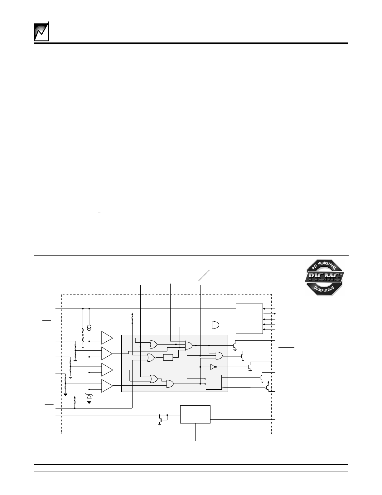
The S39421 is a fully integrated hot swap controller
intended for use on add-in cards that may be inserted into
or removed from powered-on host platforms. The S39421
performs a variety of tasks starting with the validation of
proper card insertion and the presence of “in-spec” voltages at the host platform interface.
Once power is switched on, the S39421 continues to
monitor the back-end power to the add-in card and the
host power supply. If either the 5V or 3.3V supplies drop
below Vtrip the S39421 will immediately assert the RESET outputs and power-down the add-in card.
In addition to the power control for the add-in card, the
S39421 provides status signals that can be employed by
the host and for the control of bus interface components.
The on board E2PROM can be used as configuration
memory for the individual card or as general purpose
memory. The proprietary DataDownload mode provides
a more direct interface to the E2PROM for simplified
access by the add-in card’s controller or ASIC.
FUNCTIONAL BLOCK DIAGRAM
VCC5
PND1
+
VCC3
CARD_5V
CARD_3V
PND2
ISLEW
-
+
-
+
-
+
-
VSEL
HST_PWR
Filter
Sequencing
Logic
Slew Rate
Control
HST_RST
RESET
Timer
EEPROM
Memory
Array
DD
DO
CS
SK
DI
DRVREN
SGNL_VLD
CARD_V_VLD
RESET
RESET
VGATE3
VGATE5
ASSOCIATE
MEMBER
VCC12
© SUMMIT MICROELECTRONICS, Inc. 2001 • 300 Orchard City Drive, Suite 131 • Campbell, CA 95008 • Telephone 408-378-6461 • Fax 408-378-6586 • www.summitmicro.com
Characteristics subject to change without notice
2024 9.1 1/23/01
2024 ILL2.1
1
Page 2
PIN CONFIGURATION
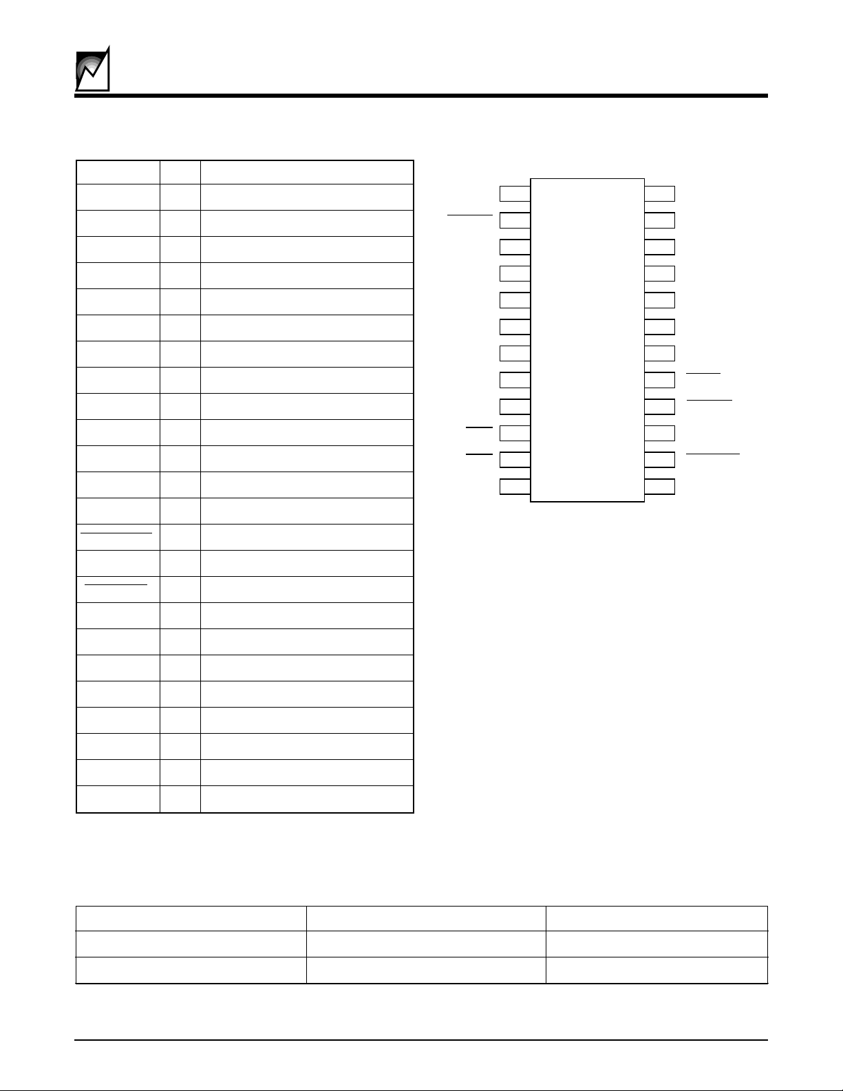
Symbol Pin Description
VCC12 1 12 Volt Input
DRVREN 2 High Side Driver Enable (L)
ISLEW 3 Slew Rate Control
VSEL 4 Voltage Select
DD 5 Data Download Enable
CS 6 Microwire Chip Select
SK 7 Microwire Serial Clock
DI 8 Microwire Data In
DO 9 Microwire Data Out
VCC12
DRVREN
ISLEW
VSEL
1
2
3
4
DD
5
CS
6
SK
7
DI
8
DO HST_RST
9
24
23
22
21
20
19
18
17
16
S39421
VCC5
VGATE5
CARD_5V
VCC3
VGATE3
CARD_3V
RESET
RESET
PND2 10 Pin Detect 2 (Active Low)
PND1 11 Pin Detect 1 (Active Low)
GND 12 Ground
CARD_V_VLD
13 Card Voltage Valid
SGNL_VLD 14 Signals Valid (Active Low)
HST_PWR 15 Host Power Up Enable
HST_RST 16 Host Reset (Active Low)
RESET 17 RESET(Active Low)
RESET 18 RESET
CARD_3V 19 Card’s 3 Volt Monitor Input
VGATE3 20 3 Volt Gate Output
VCC3 21 3 Volt Input
CARD_5V 22 Card’s 5 Volt Monitor Input
VGATE5 23 5 Volt Gate Output
VCC5 24 5 Volt Input
PND2
PND1
GND
10
11
12
15
14
CARD_V_VLD
13
HST_PWR
SGNL_VLD
2024 ILL1.1
RECOMMENDED OPERATING CONDITIONS
Condition Min Max
Temperature -40°C +85°C
V
CC
2
2.7V 5.5V
2024 9.1 1/23/01
2024 PGM T1.1
SUMMIT MICROELECTRONICS, Inc.
Page 3
S39421
ABSOLUTE MAXIMUM RATINGS*
Temperature Under Bias -55°C to +125°C
Storage Temperature -65°C to +150°C
Voltage on :
DRVREN
VCC12 15V
VCC3 7V
CARD_5V 7V
CARD_3V 7V
SGNL_VLD, CARD_V_VLD & RESET 12V
COMMENT
Stresses listed under Absolute Maximum
Ratings may cause permanent damage to
the device. These are stress ratings only, and
functional operation of the device at these or
any other conditions outside those listed in
the operational sections of this specification
is not implied. Exposure to any absolute
maximum rating for extended periods may
affect device performance and reliability.
RESET VCC +.7V
All Others VCC +.7V
Output Short Circuit Current 100mA
Lead Solder Temperature (10 secs) 300°C
DC OPERATING CHARACTERISTICS (Over Recommended Operating Conditions)
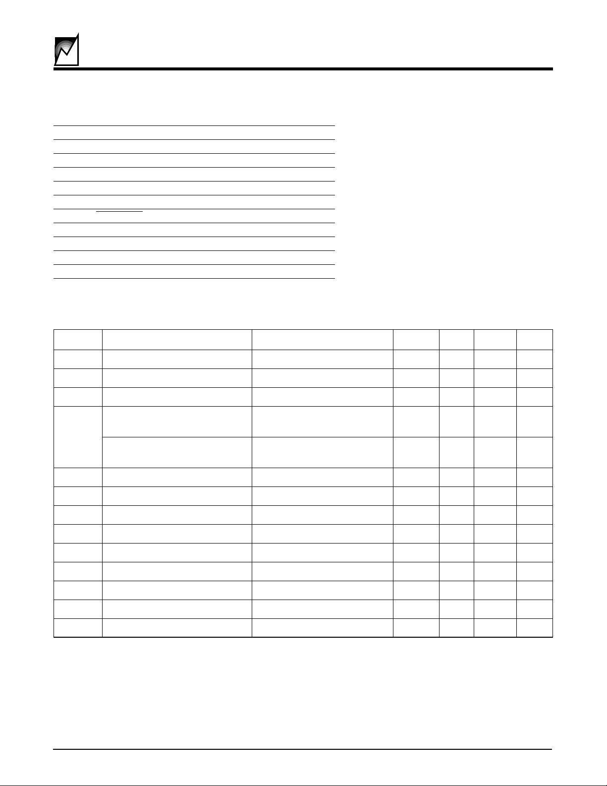
Symbol Parameter Conditions Min Typ Max Units
I
CC1
I
CC2
Power Supply Current Resets Active, VGATES Ramping .6 1 mA
Power Supply Current
Quiesent - Resets released, VGATES On
250 500 µA
I
CC3
V
TRIP
V
TRHST
I
LI
I
LO
V
IL
V
IH
V
OL
V
OH
V
OLRS
V
OHRS
Power Supply Current Quiesent - EEPROM Access .8 1.5 mA
VTRIP Sense Levels VCC5 and CARD_5V 4.5 4.6 4.75 V
Low to High
High to Low
VCC3 and CARD_3V 2.8 2.9 3.0 V
VCC5 and CARD_5V 4.5 4.70 V
VCC3 and CARD_3V 2.8 2.95 V
Trip Point Hysteresis 7 mV
Input Leakage Current 1 2 µA
Output Leakage Current 2 10 µA
Input Low Voltage -0.1 0.8 V
Input High Voltage 2 VCC+1 V
Output Low Voltage VCC = 5.0V, IOL = 2.1mA 0.4 V
Output High Voltage VCC = 5.0V, IOH = -400µA 2.4 V
RESET Output Low Voltage IOL = 3.2mA 0.4 V
RESET Output High Voltage IOH = -800 µA VCC-.75V V
2024 PGM T2.3
SUMMIT MICROELECTRONICS, Inc.
2024 9.1 1/23/01
3
Page 4
S39421
MEMORY AC OPERATING CHARACTERISTICS (Over Recommended Operating Conditions)
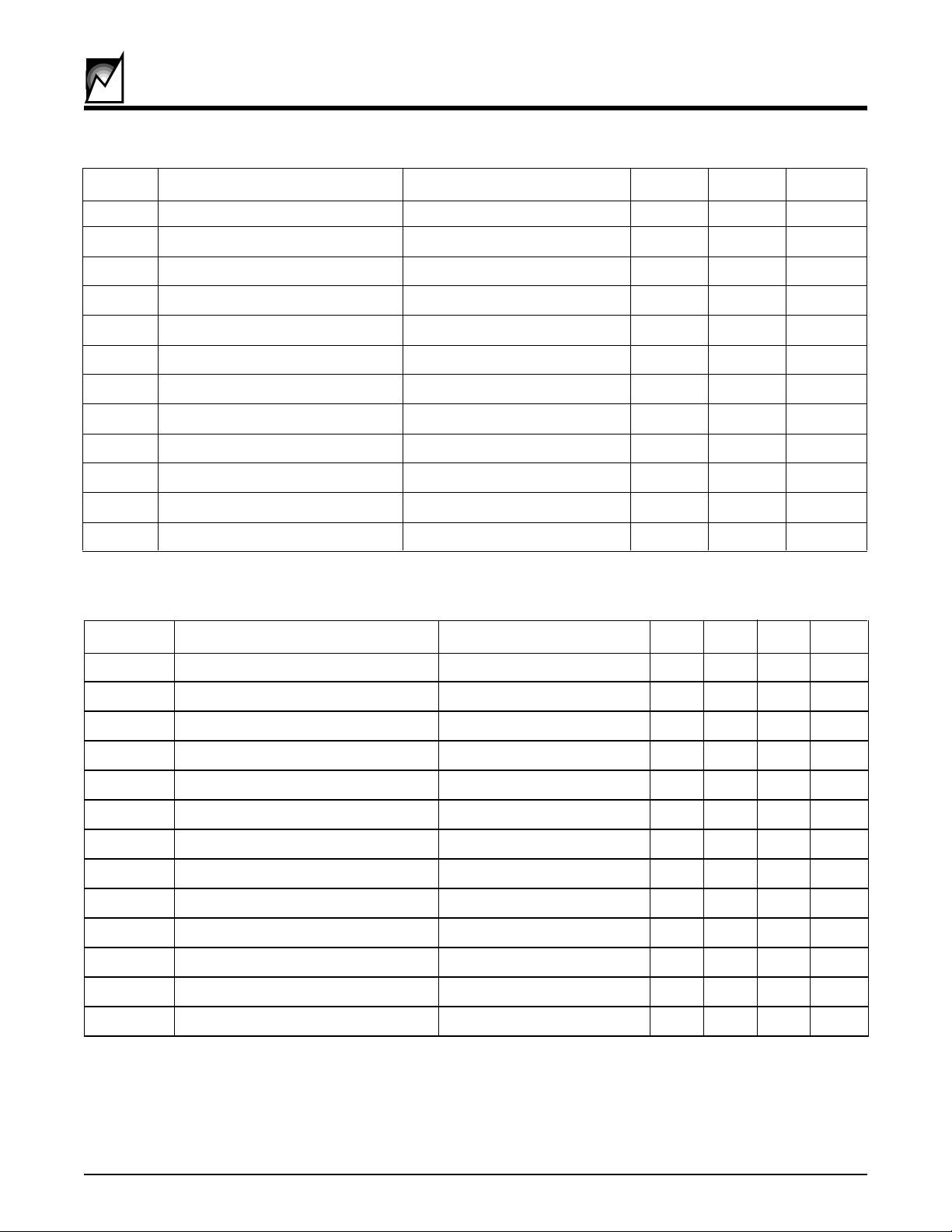
Symbol Parameter Conditions Min Max Units
t
CSS
CS Setup Time 50 ns
50
t
CSH
t
DIS
t
DIH
t
PD1
t
PD0
t
HZ
t
EW
t
CSMIN
t
SKHI
t
SV
SK
MAX
CS Hold Time 0 ns
DI Setup Time 100 ns
DI Hold Time 100 ns
Output Delay to 1 250 ns
Output Delay to 0 250 ns
Output Delay to Hi-Z 100 ns
Program/Erase Time 10 ms
Minimum CS Low Time 250 ns
Minimum SK Low Time 250 ns
Output Delay to Status Valid 250 ns
Maximum Clock Frequency 1 MHz
0
2024 PGM T3.1
SEQUENCER AC OPERATING CHARACTERISTICS (Over Recommended Operating Conditions)
Symbol Parameter Notes Min Typ Max Units
T
SLEW
Slew Rate 250 280 V/Sec
T
HSE
V
TRHST
t
PURST
V
RVALID
t
GLTICH
t
LVVG
t
LVSV
t
LVDE
t
RPD
t
CRVG
t
CRSV
t
CRDE
High Side Enable Delay Card Insertion Noise Filter 100 140 200 ms
Trip Point Hysteresis 7 mV
Power-up Reset Timeout 105 130 200 ms
RESET Output Valid 1 .9 V
Glitch Reject Pulse Width 40 ns
Loss of Voltage to V
off w. 100 pf load 2 µs
GATE
Loss of Voltage to Signal Valid off 5 µs
Loss of Voltage to Drive Enable off 20 µs
V
to RESET output Delay 5 µs
TRIP
Card Removal to V
off w. 100 pf load 2 µs
GATE
Card Removal to Signal Valid off 5 µs
Card Removal to Drive Enable off 20 µs
2024 PGM T4.4
4
2024 9.1 1/23/01
SUMMIT MICROELECTRONICS, Inc.
Page 5
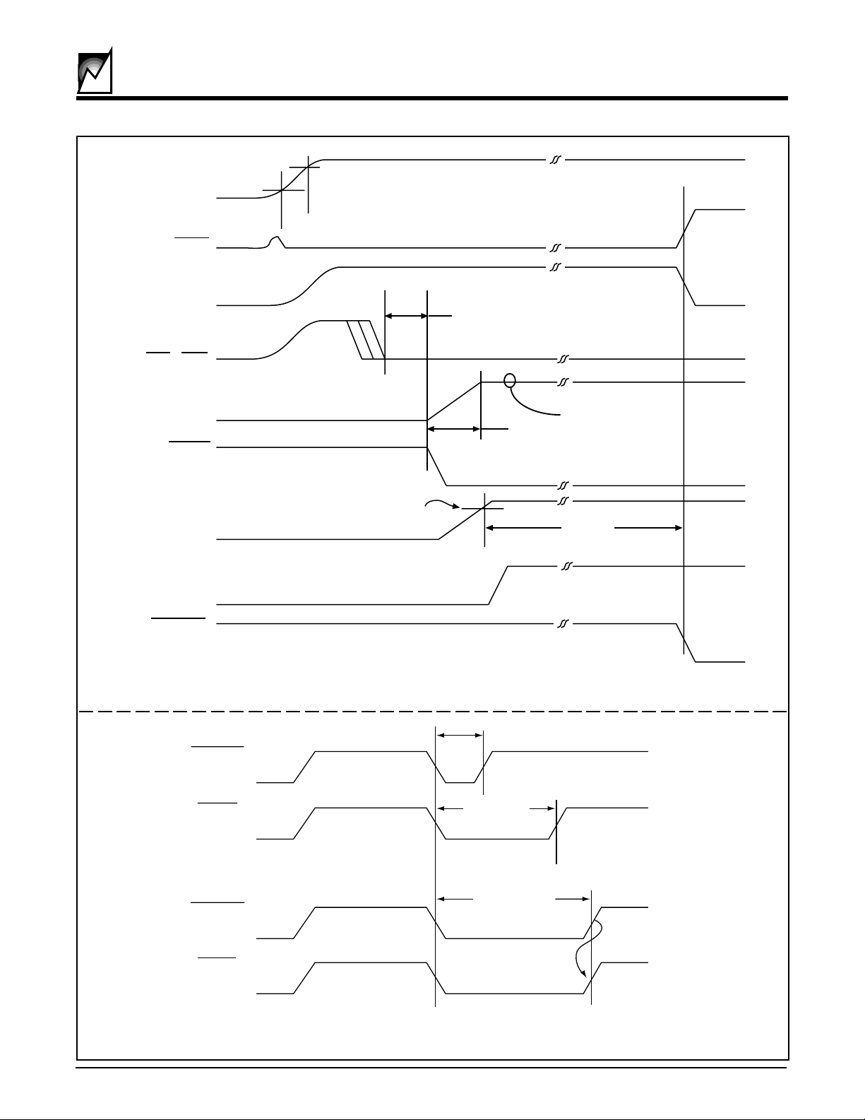
V
CC5
RESET
V
RVALID
V
TRIP5
S39421
RESET
PND1+PND2
V
CARD_5V & CARD_3V
& V
GATE5
CARD_V_VLD
SGNL_VLD
GATE3
DRVREN
V
CARD3
V
CARD5
tHSE
12V Level
tSLEW
&
tPURST
2024 ILL3.1
HST_RST
[input]
RESET
[output]
HST_RST
[input]
RESET
[output]
SUMMIT MICROELECTRONICS, Inc.
<tPURST
=tPURST
>tPURST
2024 ILL31.0
FIGURE 1. CARD INSERTION AND HOST RESET TIMING DIAGRAM
2024 9.1 1/23/01
5
Page 6
VCC5
S39421
12V
VGATE5 & VGATE3
SGNLVLD
DRVEN
CARD5V
CARD_V_VLD & RESET
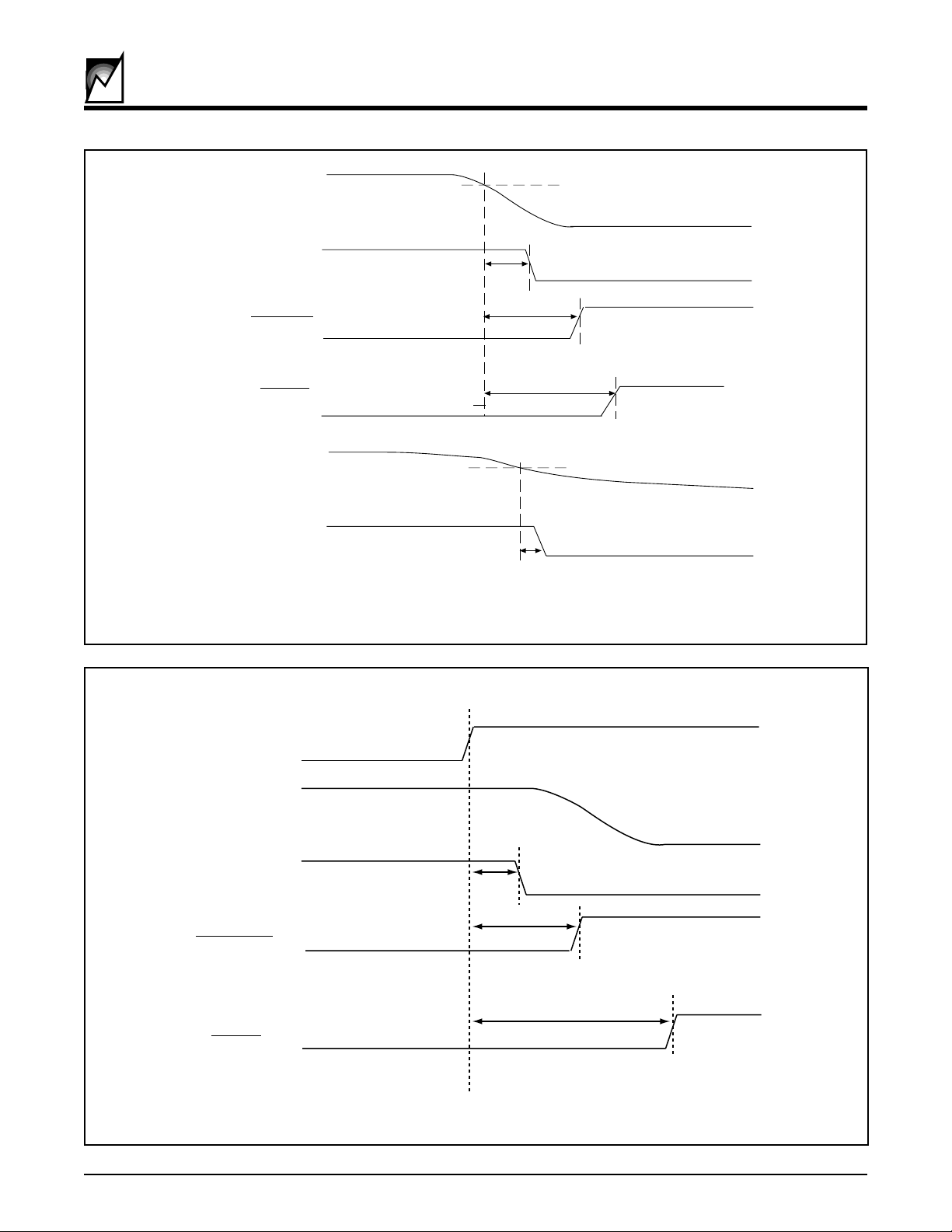
FIGURE 2. LOSS OF VOLTAGE TIMING SEQUENCE
tLVVG
tLVSV
tLVDE
tRPD
2024 ILL4.2
PinD1+PinD2
VCC5
12V
VGATE5 & VGATE3
tCRVG
tCRSV
SGNL_VLD
DRVEN
FIGURE 3. CARD REMOVAL TIMING SEQUENCE
6
tCRDE
2024 9.1 1/23/01
2024 ILL5.2
SUMMIT MICROELECTRONICS, Inc.
Page 7
S39421
PIN DESCRIPTIONS
PIN NAME [
CompactPCI
name] (pin #)
VCC12 (Pin 1): Supplies the 12 volts required for power-
ing the high-side drivers.
DRVREN (Pin 2): Open drain, active low output indicates
the status of the 3 volt and 5 volt high side driver outputs
(VGATE5 and VGATE3). This signal may also be used as
a switching signal for the 12 volt supply.
ISLEW (Pin 3): Diode-connected NFET input may be
used to adjust the 250V/s default slew rate of the high-side
driver outputs. One quarter of the current injected into this
pin will be mirrored into each of the high-side driver
outputs.
VSEL (Pin 4): TTL level input used to determine which of
the Host power supply inputs will be monitored for valid
voltage and reset generation.
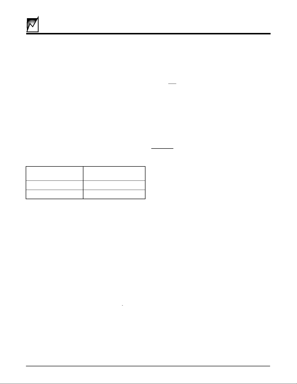
VSEL-Voltage Host Voltage
Select Monitored
Low 5 Volt or Mixed-Mode
High 3.3 Volt Only
DD (Pin 5): A high going edge on this input will place the
embedded memory into Data Download mode. This
mode allows the entire contents of the E2PROM array to
be read out of the device by selecting the device (CS high)
and providing clock cycles on the SK input. Data Down-
load mode is exited when Chip Select is brought low.
CS (Pin 6): E2PROM memory chip select, active high.
SK (Pin 7): E2PROM memory serial clock input.
DI (Pin 8): E2PROM memory data input.
DO (Pin 9): E2PROM memory data output.
PND2 [BD_SEL2#] (Pin 10): Active low TTL level input
with internal pull-up to VCC5. In conjunction with PND1,
this signal indicates proper card insertion. This pin must
be connected to ground on the host side of the connector.
PND1 and PND2 must be placed on opposite corners of
the connector and will preferably be staggered shorter
than the power connector pins. Board insertion is assumed when PND1 and PND2 are low.
PND1 [BD_SEL1#] (Pin 11): Active low TTL level input
with internal pull-up to VCC5. In conjunction with PND2,
this signal indicates proper card insertion.
GND (Pin 12): Ground.
CARD_V_VLD (pin13): CARD_V_VLD is an open drain
output, indicating the card side voltages are at or above
V
.
TRIP
SGNL_VLD (Pin 14): Signals valid (SGNL_VLD) is an
open drain active low signal indicating the card side power
is valid and that the reset signals have been released.
This signal can be used by the host as an indication that
the bus interface is active and all signals are valid.
HST_PWR (pin15): The host power (HST_PWR) input is
an active high input. It provides the host system active
control over the sequencing of the power up operation.
When low, the S39421 will hold the add-in card in reset
and block all power to the backend logic. When
HST_PWR is high the power sequencing will begin immediately and the reset outputs will be driven active after
t
.
PURST
HST_RST [PCI_RST#] (Pin 16): TTL level input used as
a reset input signal from the host interface. An active low
level longer than 40 nsec will cause a reset sequence to
be performed on the card. The power switching logic will
not be affected.
RESET (Pin 17): RESET is an active low open-drain
output. It should be tied high through a pull-up resistor
connected to VCC.
RESET (Pin 18): RESET is an active high open drain
(PFET) output. It should be tied low through a pull-down
resistor connected to ground.
CARD_3V (Pin 19): 3.3 volt card side supply input. This
input is monitored for power integrity. If it falls below the
3.3V sense threshold, the PWR_VLD signal is de-asserted and a RESET sequence initiates.
VGATE3 (Pin 20): Slew rate limited high side driver
output for the 3.3V external Power FET gate.
VCC3 (Pin 21): 3.3 volt host side supply input. This input
is monitored for power integrity. If it falls below the 3.3V
sense threshold, the SGNL_VLD signal is de-asserted
and the high side drivers disabled.
CARD_5V (Pin 22): 5 volt card side supply input. This
input is monitored for power integrity. If it falls below the
5V sense threshold and the VSEL input is low, the
PWR_VLD signal is de-asserted and a RESET sequence
initiates.
VGATE5 (Pin 23): Slew rate limited high side driver
output for the 5V external Power FET gate.
VCC5 (Pin 24): Power to the S39421 and 5 volt host side
supply input. This input is monitored for power integrity. If
it falls below the 5V sense threshold and the VSEL input
is low, the SGNL_VLD signal is de-asserted and the high
side drivers disabled.
SUMMIT MICROELECTRONICS, Inc.
2024 9.1 1/23/01
7
Page 8

S39421
DEVICE OPERATION
Power-Up Sequence
A sequencing operation is initiated by the physical insertion of the card into the platform’s connector. The
S39421’s VCC5 pin should be connected to the early
power pins of the connector. As soon as power is applied,
the S39421 will drive the reset outputs active and clamp
the VGATE outputs to ground.
Proper card insertion is insured by detecting the presence
of a low level on the pin detect (PND1, PND2) inputs,
which should be located on opposite ends of the bus
connector. These pin detect inputs have internal pull-up
resistors and the connection on the host platform side
must be connected directly to ground. [In a
CompactPCI
application these are the BD_SEL# signals]. The PND
inputs have an internal noise filter nominally set at 150ms.
Once the proper card insertion has been detected, the
S39421 will check the status of the HST_PWR signal from
the host.
Implementation of HST_PWR is optional; e.g. it can be
used to power down individual cards on the bus via
software control. If it is not used by the host system the
input must be held high in order for the S39421 to enable
power sequencing to the card.
Once these basic conditions are met the S39421 will
begin the power-up portion of the sequence. First, the
host platform supplies are checked for compliance.
Based on the state of the VSEL input the S39421 will
monitor the +5V and +3.3V supplies. If these are above
the VTRIP thresholds the sequencing next begins the
backend logic power-on operation.
The S39421 will drive the VGATE3 and VGATE5 outputs
to the 12V rail to turn on the external 3 volt and 5 volt power
FETs. The slew rate of these outputs defaults to 250V/s.
Different slew rates can be accommodated by either
adding an additional capacitor between the FET gate and
ground or by injecting current into the ISLEW input.
RESET CONTROL
In order to provide positive control to an add-in-card’s
bakckend logic, the reset control function of the S39421
begins operation as soon as a voltage is applied to VCC5.
The conditions that affect the reset outputs are the VCC5,
VCC3, CARD_5V and CARD_3V input levels and the
state of the HST_RST input.
Assume HST_RST has been released and is pulled high.
The S39421 reset ouputs will be valid as long as VCC5
is • 1V. If any one of VCC5, VCC3, CARD_5V or
CARD_3V input levels is below its respective Vtrip level
the reset outputs and CARD_V_VLD output will be driven
active. (In the case of the CARD_V_VLD output, the
active condition is low but its logical true condition is a
release of its open drain output pulled high by an external
pull-up) As soon as the VCC5, VCC3, CARD_5V and
CARD_3V inputs are above their Vtrip levels
CARD_V_VLD will be released and the internal tPURST
timer will be started. The reset outputs will be held active
until tPURST has expired and then be released.
The HST_RST input is also used to control the reset
outputs. A high to low transition on HST_RST will initiate
a reset cycle with a duration of tPURST. The reset outputs
will remain active for a minimum period tPURST or for the
duration of HST_RST active low, whichever is longer. A
HST_RST activated reset will not affect the power sequencing logic.
During normal operation, the supply voltages are continuously monitored. If the cardside supplies fall below the
VTRIP levels the reset outputs will be driven active. If the
host platform supplies fall below VTRIP, the S39421 will
immediately assert the reset outputs and disable the
highside drivers.
Power Configurations
The S39421 can be used in 5V-only, 3.3V-only and mixed
voltage systems. For mixed voltage systems, simply
connect the appropriate bus and card power inputs as
indicated. The VSEL pin should be grounded.
For systems with a single power supply, connect VCC5
and VCC3 together to the platform host early power line
(long pin power supply). Also connect CARD5V and
CARD3V together to the cardside power output of the
FET.
The state of VSEL determines the reset level that will be
used to signal CARD_V_VLD. For 3.3V systems, tie
VSEL to the supply; for 5V systems, tie VSEL to ground.
8
2024 9.1 1/23/01
SUMMIT MICROELECTRONICS, Inc.
Page 9
VCC5 ≥ 1V
S39421
ASSERT
RESET
OUTPUTS
SHUT OFF
VGTE5
VGTE3
DRVREN
PWR_VLD
SGNL-VLD
PND1
&
PND2?
YES
VSEL
HI ?
NO
NO
HOST
5V & 3V
OK?
YES
TURN-ON
VGTE5
VGTE3
DRVREN
CARD 5V & 3V
OK?
YES
START
RESET
TIMER
NO
NO
TURN ON
PWR_VLD
NO
3VOLT
OK?
SUMMIT MICROELECTRONICS, Inc.
YES
YES
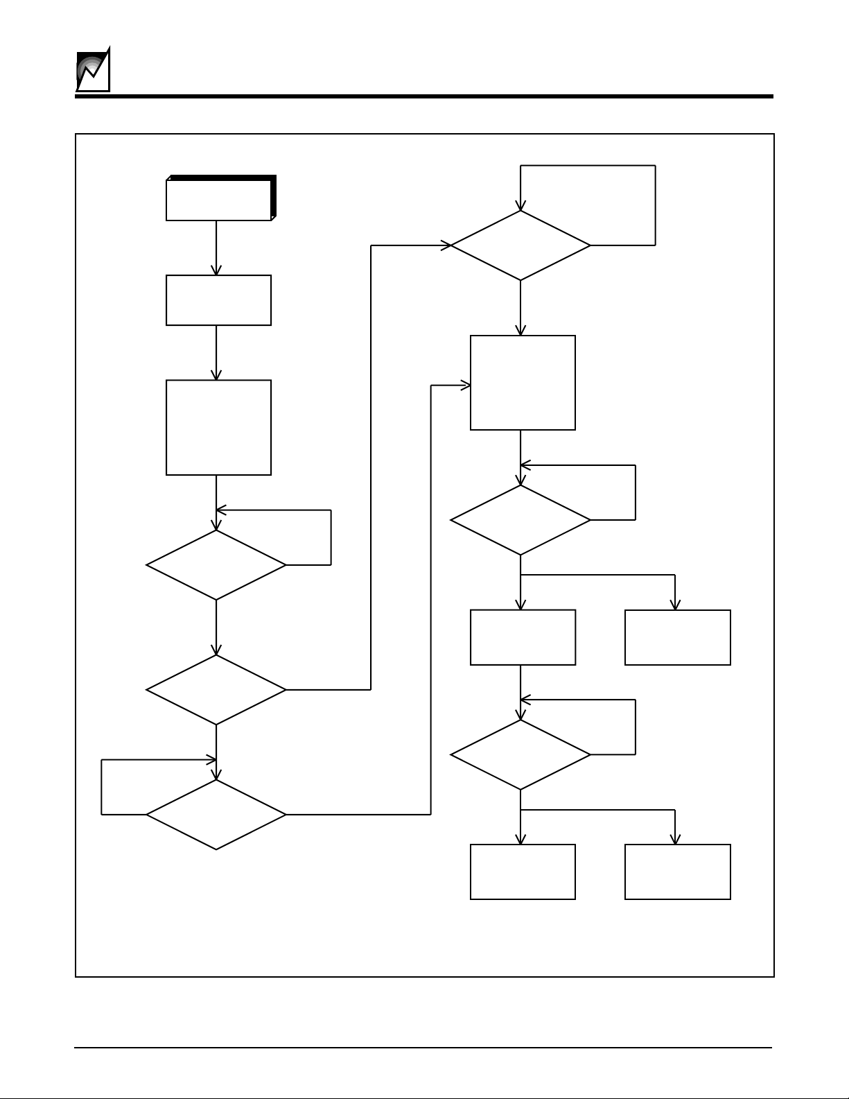
FIGURE 4.
2024 9.1 1/23/01
tPURST
TIMEOUT?
YESHOST
RELEASE
RESETS
NO
TURN ON
SGNL_VLD
2024 ILL6.2
9
Page 10
S39421
MEMORY OPERATION
The S39421 has a 1024-bit nonvolatile memory
intended for use with industry standard microprocessors.
The memory is organized as X16, seven 9-bit instructions
control the reading, writing and erase operations of the
device. The device operates on a single 3V or 5V supply
and will generate on chip, the high voltage required during
any write operation.
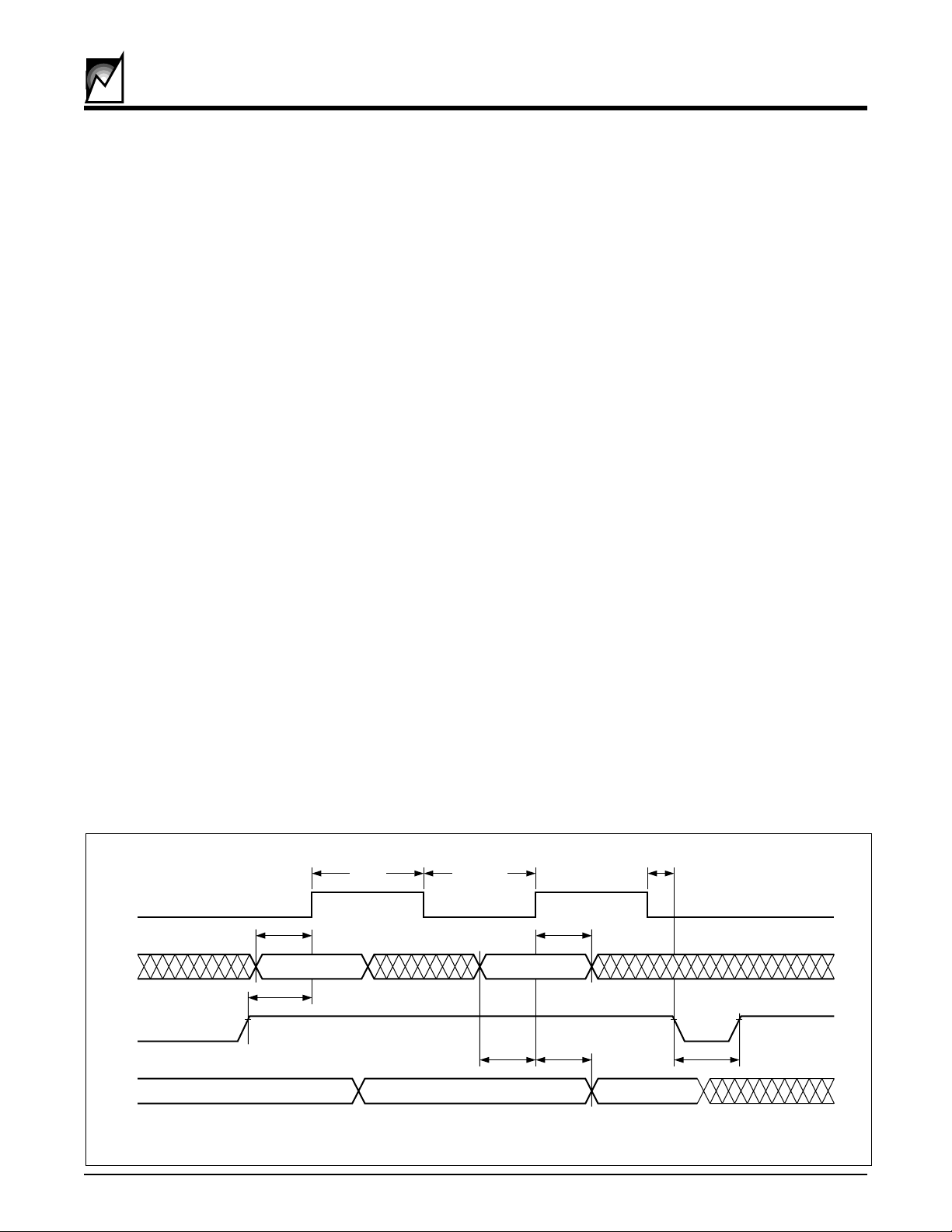
Instructions, addresses, and write data are clocked into
the DI pin on the rising edge of the clock (SK). The DO pin
is normally in a high impedance state except when reading data from the device, or when checking the ready/busy
status after a write operation.
The ready/busy status can be determined after the start of
a write operation by selecting the memory and polling the
DO pin; DO low indicates that the write operation is not
completed, while DO high indicates that the device is
ready for the next instruction.
The format for all instructions is: one start bit; two op code
bits and either six address or instruction bits.
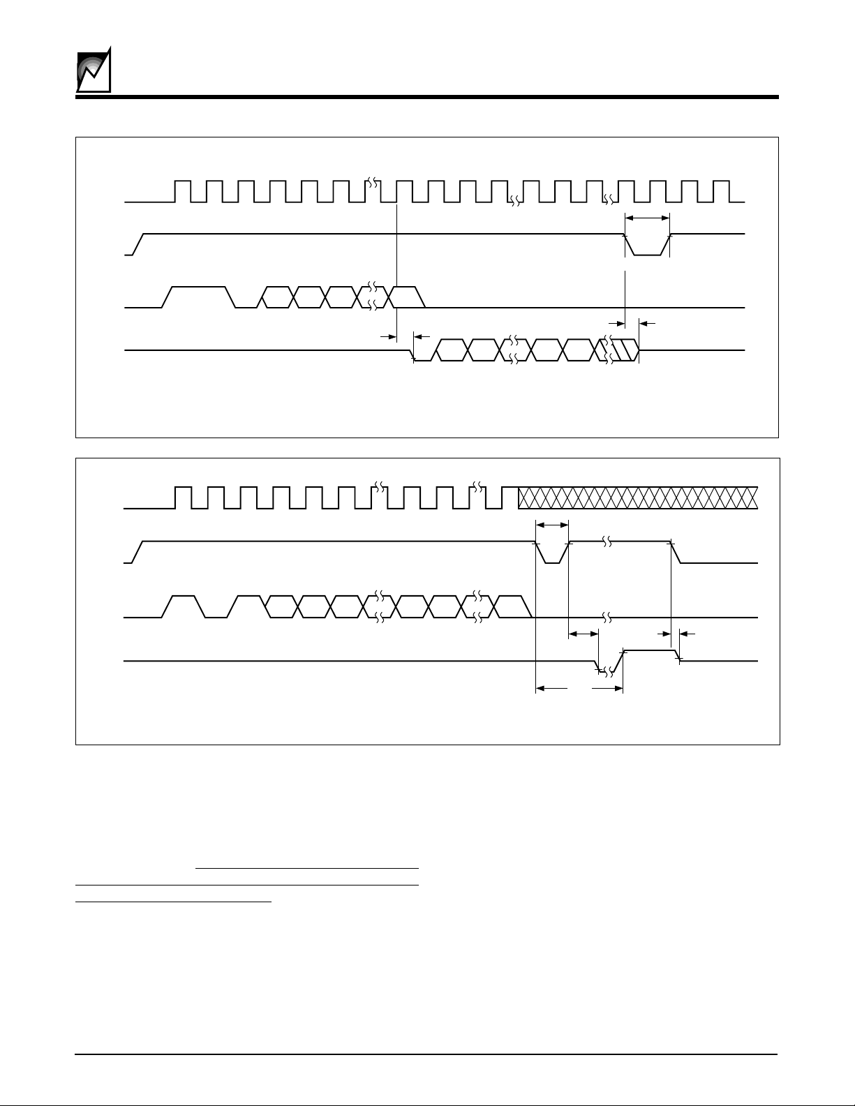
Read
Upon receiving a READ command and an address
(clocked into the DI pin), the DO pin will come out of the
high impedance state and, will first output an initial dummy
zero bit, then begin shifting out the data addressed (MSB
first). The output data bits will toggle on the rising edge of
the SK clock and are stable after the specified time delay
(t
PD0
or t
PD1
).
Continuous Read
This begins just like a standard read with the host issuing
a read instruction and clocking out the data byte [word]. If
the host then keeps CS high and continues generating
clocks on SK, the S39421 will output data from the next
higher address location. The S39421 will continue
incrementing the address and outputting data so long as
CS stays high. If the highest address is reached, the
address counter will roll over to address 0000. CS going
low will reset the instruction register and any subsequent
read must be initiated in the normal manner of issuing the
command and address.
Write
After receiving a WRITE command, address and the data,
the CS (Chip Select) pin must be deselected for a minimum of 250ns (t
). The falling edge of CS will start
CSMIN
automatic write cycle to the memory location specified in
the instruction. The ready/busy status can be determined
by selecting the device and polling the DO pin.
Page Write
Assume WEN has been issued. The host will then take CS
high, and begin clocking in the start bit, write command
and 6-bit address immediately followed by the first 16-bit
word of data to be written. The host can then continue
clocking in 16-bit words of data with each word to be
written to the next higher address. Internally the address
pointer is incremented after receiving each group of
sixteen clocks; however, once the address counter
reaches xxx x111 it will roll over to xx x000 with the next
clock. After the last bit is clocked in no internal write
operation will occur until CS is brought low.
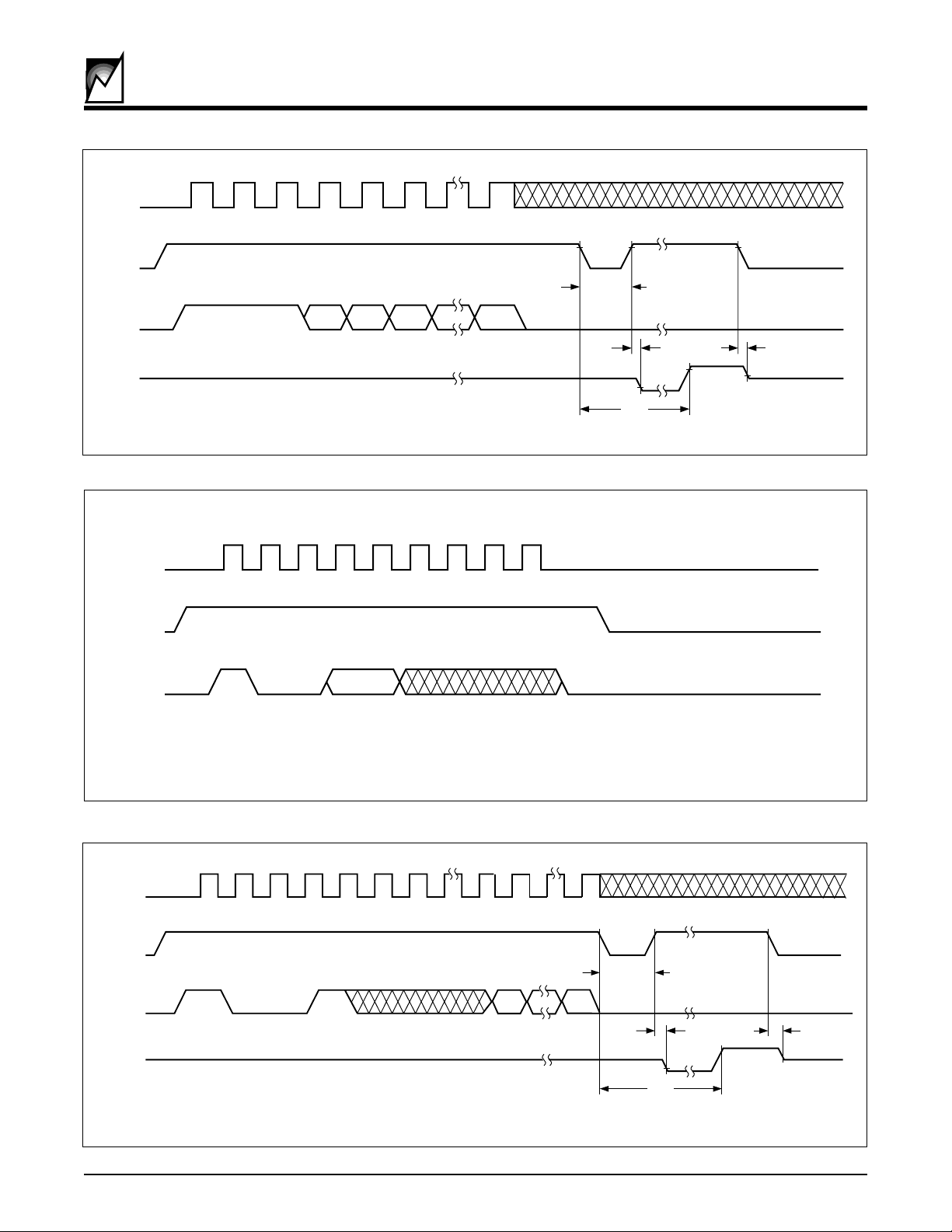
Erase
Upon receiving an ERASE command and address, the
CS (Chip Select) pin must be deselected for a minimum
of 250ns (t
). The falling edge of CS will start the auto
CSMIN
erase cycle of the selected memory location. The ready/
busy status can be determined by selecting the device
and polling the DO pin. Once cleared, the content of a
cleared location returns to a logical “1” state.
10
SK
CS
DO
t
t
SKHI
t
DIS
DI
t
CSS
VALID VALID
FIGURE 5. SYCHRONOUS DATA TIMING
SKLOW
t
DIS
2024 9.1 1/23/01
t
DIH
t
PD0,tPD1
DATA VALID
t
CSH
t
CSMIN
2024 ILL19.0
SUMMIT MICROELECTRONICS, Inc.
Page 11
SK
CS
DI
DO
11 0
ANA
N–1
t
PD0
A
0
0
DND
FIGURE 6. READ INSTRUCTION TIMING
N–1
D1D
S39421
t
CS
STANDBY
t
HZ
0
HIGH-ZHIGH-Z
2024 ILL20.0
SK
CS
DI
DO
101
ANA
N-1
HIGH-Z
A
FIGURE 7. WRITE INSTRUCTION TIMING
Erase/Write Enable and Disable
The memory powers up in the write disable state. Any
writing after power-up or after an EWDS (write disable)
instruction must first be preceded by the EWEN (write
enable) instruction. Once the write instruction is enabled,
it will remain enabled until power to the device is removed,
or the EWDS instruction is sent. The EWDS instruction
can be used to disable all S39421 write and clear instructions, and will prevent any accidental writing or clearing of
the device. Data can be read normally from the device
regardless of the write enable/disable status.
t
CS
STATUS
VERIFY
D
0
N
D
0
t
SV
t
EW
BUSY
READY
STANDBY
t
HZ
HIGH-Z
2024 ILL21.0
Write All
Upon receiving a WRAL command and data, the CS (Chip
Select) pin must be deselected for a minimum of 250ns
(t
). The falling edge of CS will start the self clocking
CSMIN
data write to all memory locations in the device. The
clocking of the SK pin is not necessary after the device has
entered the self clocking mode. The ready/busy status of
the S39421 can be determined by selecting the device
and polling the DO pin. It is not necessary for all memory
locations to be cleared before the WRAL command is
executed.
SUMMIT MICROELECTRONICS, Inc.
2024 9.1 1/23/01
11
Page 12
SK
S39421
CS
DO
STATUS VERIFY
t
A
A
N
N-1
DI
11
1
A
0
t
SV
HIGH-Z
CS
BUSY READY
t
EW
FIGURE 8. ERASE INSTRUCTION TIMING
STANDBY
t
HZ
HIGH-Z
2024 ILL22.0
SK
CS
DI
10
0
*
STANDBY
SK
CS
DO
* ENABLE = 11
DISABLE = 00
2024 Fig09
FIGURE 9. EWEN/EWDS INSTRUCTION TIMING
STATUS VERIFY
t
CS
DI
10 1
00
D
N
D
O
t
SV
BUSY READY
t
EW
FIGURE 10. WRAL INSTRUCTION TIMING
STANDBY
t
HZ
HIGH-Z
2024 ILL24.0
12
2024 9.1 1/23/01
SUMMIT MICROELECTRONICS, Inc.
Page 13
S39421
INSTRUCTION SET
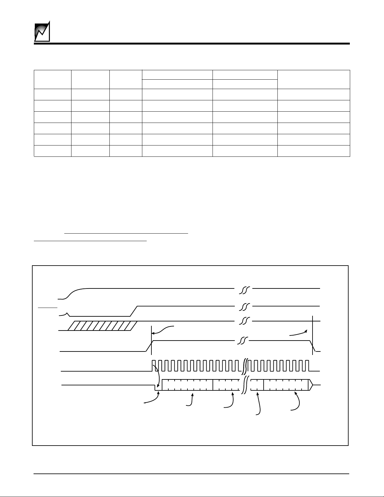
Instruction Start Opcode Address Data Comments
Bit x16 x16
READ 1 10 A5 - A0 Read Address AN–A0
ERASE 1 11 A5 - A0 Clear Address AN–A0
WRITE 1 01 A5 - A0 D15–D0 Write Address AN–A0
EWEN 1 00 11xxxx Write Enable
EWDS 1 00 00xxxx Write Disable
WRAL 1 00 01xxxx D15–D0 Write All Addresses
2024 PGM T5 .0
Data Download Mode
The Data Download mode is an alternative method of
accessing the E2PROM memory. Use of this mode allows
downloading the entire contents of the memory without
entering any commands. The DD mode is enabled after a
low to high transition on the DD pin, while continuing to
assert DD (this includes powering up the device with DD
tied high). Also, as a condition to enter this mode, the
device must not be in a state of reset. Once in Data
Download mode, the device will wait until Chip Select is
VCC
RESET
DD
DD Mode Enabled After
RESET is released and After
DD is Taken to Logic 1
CS
driven active. At this point, the device will output a dummy
‘0’ followed by the contents of location 0000. As long as
the SK line is toggled the S39421 will continue to output
the contents of sequential address locations. In this
manner, the configuration data that is loaded into an
interface device can be accessed in a simple manner
without requiring the logic of the interface chip to generate
the complex signals needed for the microwire interface.
Data Download mode is exited upon the first high to low
transition of the Chip Select input.
DD Mode
Disabled
SK
DO
SUMMIT MICROELECTRONICS, Inc.
Dummy 0
FIGURE 11. DATA DOWNLOADER SEQUENCE OF OPERATION
[note: all data download timing conforms to the timing shown in Figure 5]
Data From
Address 000
2024 9.1 1/23/01
Data From
Address 001
Data From
Address 1FE
Data From
Address 1FF
2024 ILL7.1
13
Page 14
S39421
Data Download Control
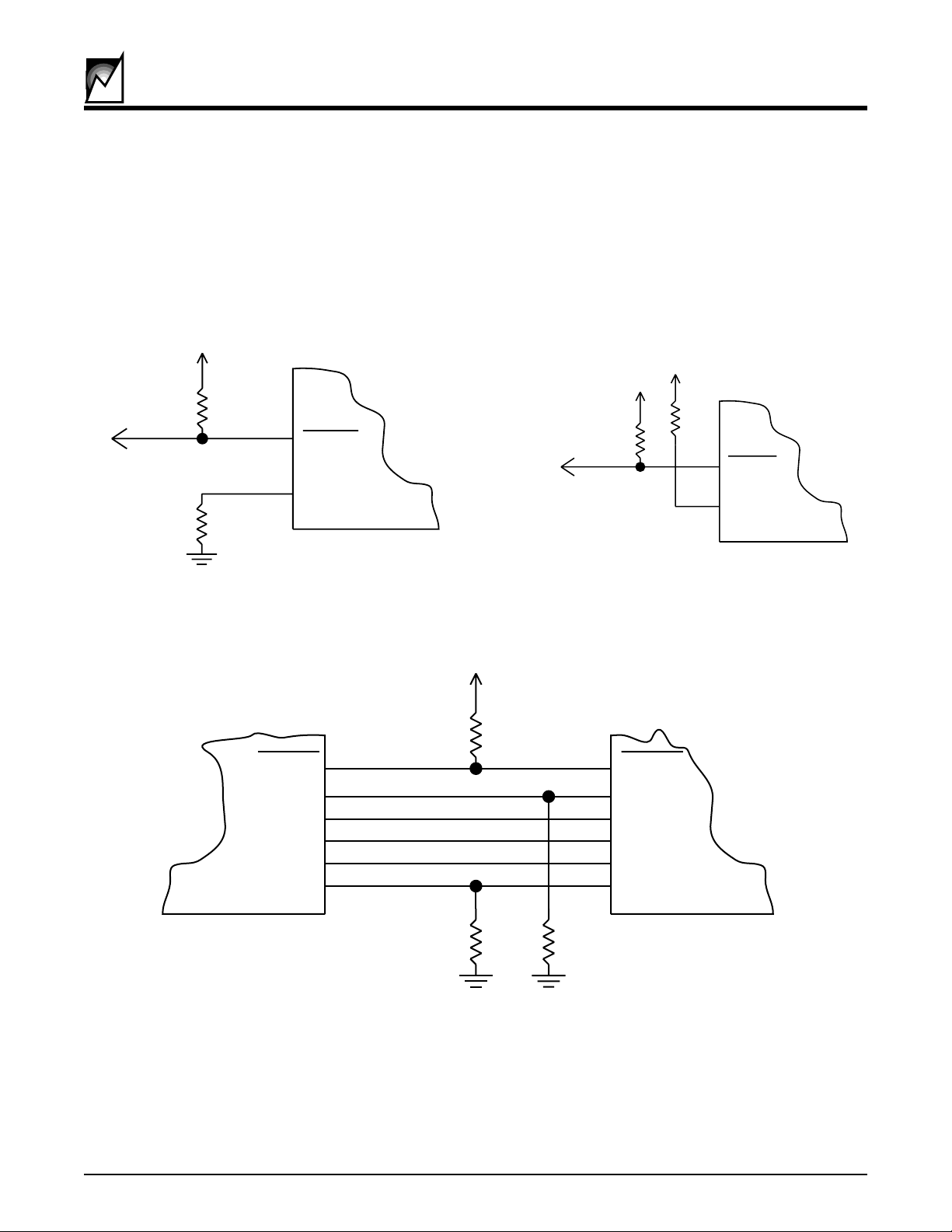
There are a number of ways to implement the data
download mode of operation. For applications that do not
require use of this feature, simply ground the DD pin and
disable the function altogether.
RESET
System
Reset
DD
2024 ILL8.0
In Figure 13, DD is tied to VCC through a pull-up resistor.
This will allow only a single download after power on. The
actual download function would not be enabled until
had expired and CS was brought high. As soon as
t
PURST
CS is deselected the DD mode will be disabled. The
primary disadvantage to this method is the lack of a reload
after brownout. The DD mode may or may not be initiated
depending on how low the power is cycled.
System
Reset
RESET
DD
2024 ILL9.0
FIGURE 12. DD DISABLED
RESET
I/Oe
ASIC
I/Oa
I/Ob
I/Oc
I/Od
FIGURE 13. ONE TIME DOWNLOAD
RESET
DD
SK
DO
DI
CS
2024 ILL10.0
FIGURE 14. ASIC CONTROL
In Figure 14, the S39421 DD mode is 100% under the control of the add-in board’s ASIC. The pull-down resistors insure
CS and DD do not float while the ASIC is in a reset state or shortly thereafter, which may lead to spurious activity on
CS and DD, possibly indicating a false DD request.
14
2024 9.1 1/23/01
SUMMIT MICROELECTRONICS, Inc.
Page 15
S39421
RESET
I/Oe
ASIC
I/Oa
I/Ob
I/Oc
I/Od
FIGURE 15. DOWNLOAD ENABLED IN CONJUNCTION WITH RESET RELEASE
RESET
DD
SK
DO
DI
CS
2024 ILL11.0
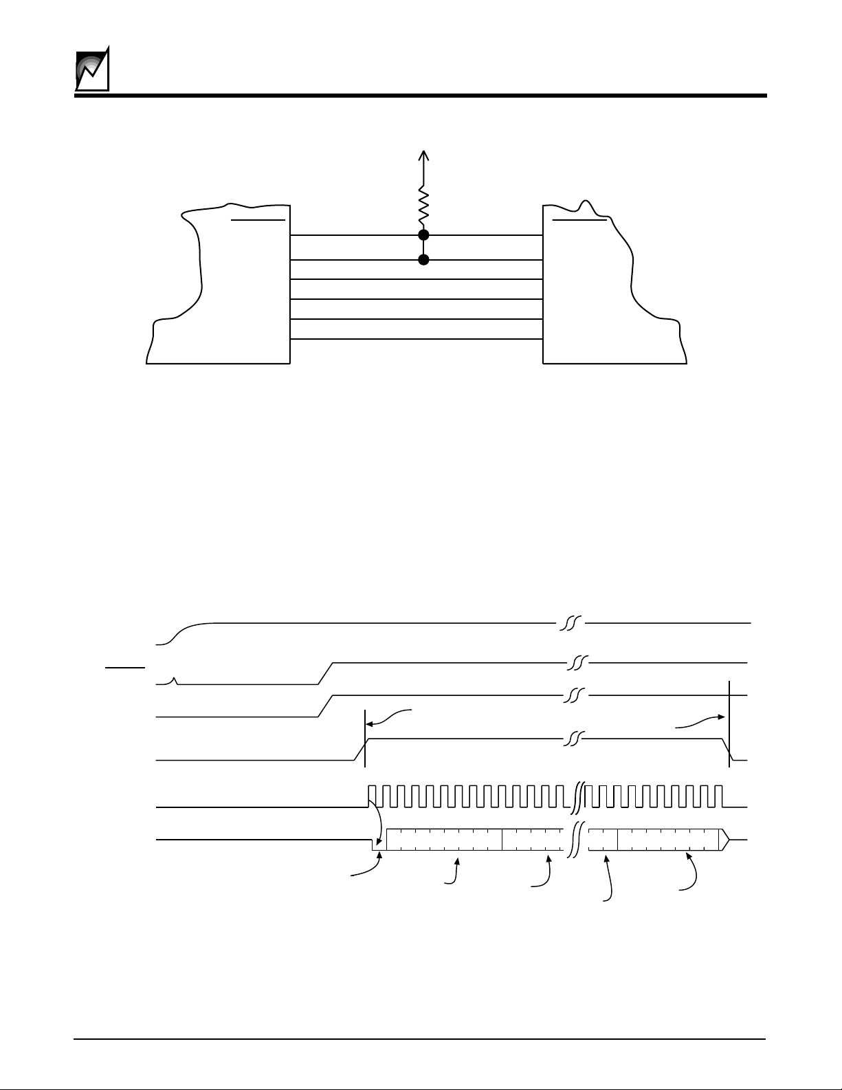
Figure 15 is a good implementation to use whenever there is a requirement to download data from the memory after
any reset cycle. This provides control of the DD input function after power-on, brown-out or a system induced reset
condition. In this way the data download function is ready under any circumstance an ASIC or MCU might need to
reload initialization data.
VCC
RESET
DD
CS
SK
DO
SUMMIT MICROELECTRONICS, Inc.
DD Mode
Enabled
Dummy 0
FIGURE 16. DD CIRCUIT 4 TIMING SEQUENCE DIAGRAM
Data From
Address 000
2024 9.1 1/23/01
Data From
Address 001
Data From
Address 1FE
DD Mode
Disabled
Data From
Address 1FF
2024 ILL12.0
15
Page 16
S39421
Slew Rate Control
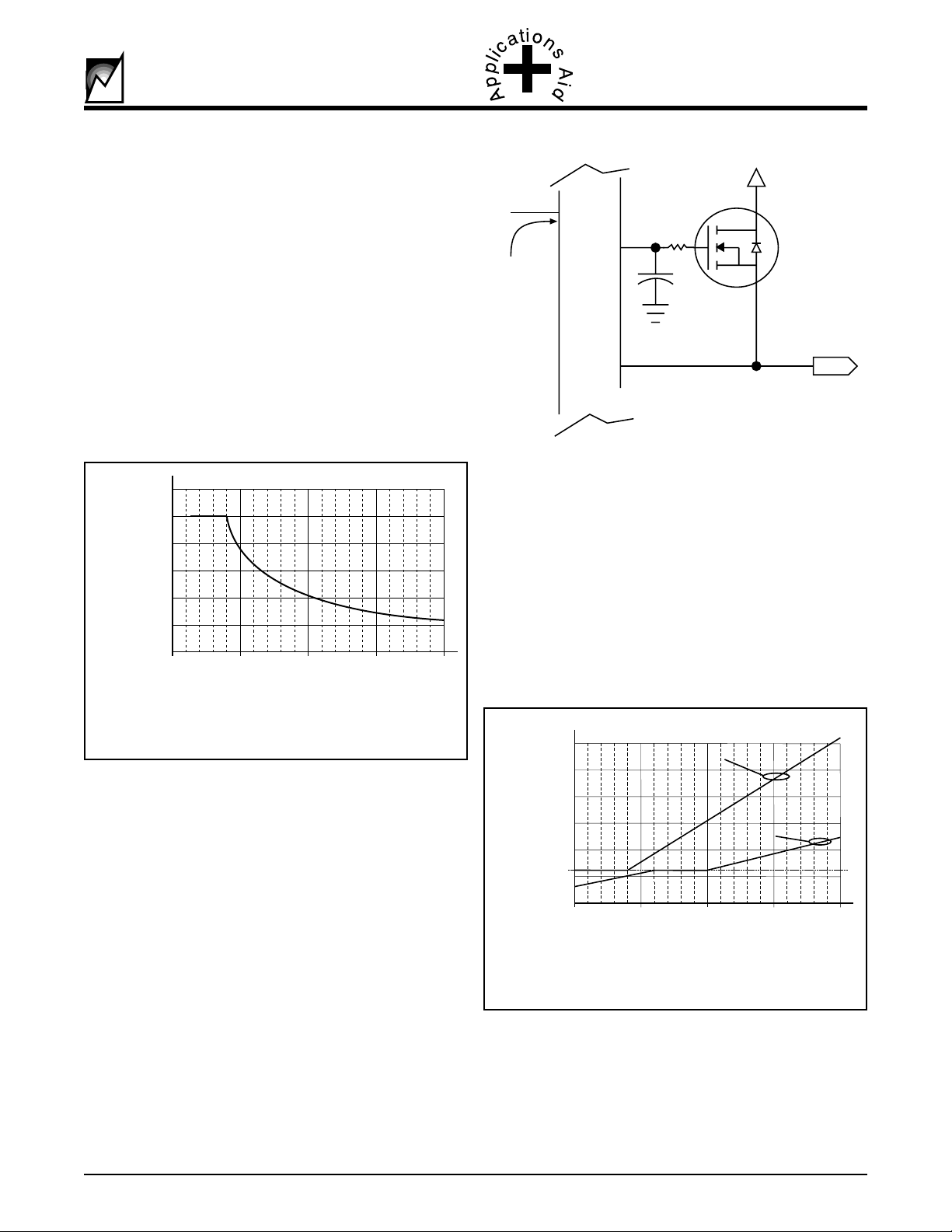
The nominal slew rate for the VGATE3 and VGATE5
outputs is set at a default value of 250V per second, which
conforms to a number of standards including that for
Compact PCI. This slew rate helps limit current spike
transients as the bypass capacitors of the add-in card are
charged. The conditions for the default slew rate are:
ISLEW input is grounded; and the C
capacitance is
VGATE
less than or equal to 0.08µF.
The slew rate can be extended (made slower) by adding
capacitance to the VGATE outputs. In this case it should
be assumed the I
input is grounded. The VGATE
SLEW
outputs can drive up to 20µA typically, so the slew rate may
be calculated as 20µA ÷ C
(not exceeding 250V/s).
VGATE
Refer to Graph 1 shown below.
300
250
200
150
100
50
Slew Rate (V/s)
0
0 0.1 0.2 0.3 0.4
Capacitance (µF)
2024 ILL13.0
FIGURE 17
Host 5V
3
I
SLEW
10Ω
VGTE5
ISLEW IN
S39421
VOUT5
23
22
FIGURE 18
C
VGATE
To Card 5V
2024 ILL14.1
The slew rate can be increased (made faster) by injecting
current into the ISLEW input. One quarter of the current
injected into ISLEW will be mirrored out of the VGATE
drivers. The resulting slew rate may be calculated as
I
SLEW
÷ 4xC
(not less than 250V/s). Example slew
VGATE
rates are plotted to illustrate the effects of capacitance on
the VGATE output in Graph 2. The reason for the flat
portion of the graph is that the internal slew rate control
operates in parallel to add as much as 20µA (typically) to
help keep the SR at 250V/s.
1200
1000
C = 0.08µF
16
Note that the ISLEW input is simply a diode-connected
MOSFET. As a consequence, its I-V characteristic is
temperature dependent.
2024 9.1 1/23/01
800
600
400
200
Slew Rate (V/s)
0
0 100 200 300 400
I
SLEW
FIGURE 19
C = 0.2µF
250V/s
Current in µA
SUMMIT MICROELECTRONICS, Inc.
2024 ILL15.0
Page 17
Card Power-Down
S39421
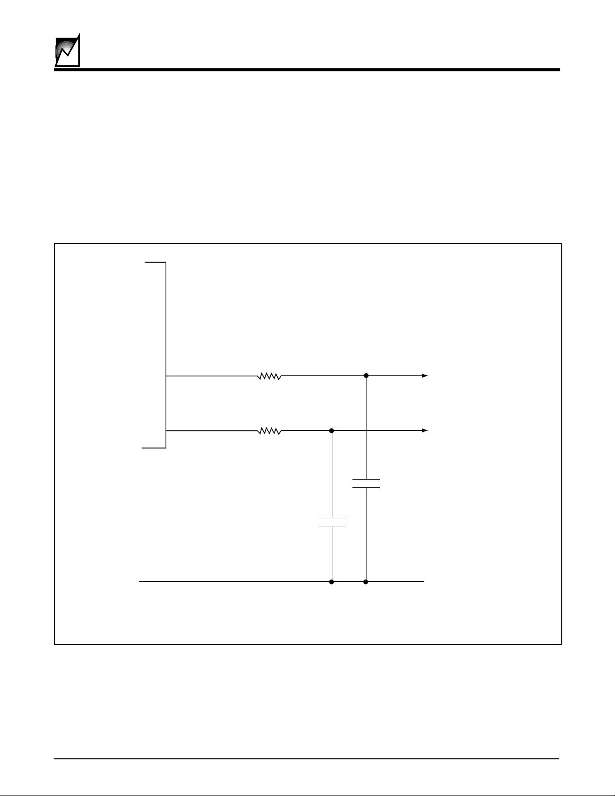
The S39421 provides a turn-on slew-rate of 250V/s and a
fast turn-off performed by internally shorting the VGATE3
and VGATE5 outputs to ground. If the card circuitry or
host power supply cannot accept a fast shutdown then a
CR time constant may be added as shown below. The
VGATE3
S39421/4
56kΩ
VGATE5
resistors in series with the 47nF(X7R) capacitors increase
the discharge time of the MOSFET gates. The values
shown provide a shutdown slew of ~5V/ms. Decreasing
the resistor values increases the shutdown slew-rate, and
vice-versa. The capacitor values may also be increased
but this will decrease the 250V/s turn-on slew-rate.
to 3V MOSFET
to 5V MOSFET
56kΩ
47nF
GND
FIGURE 20. POWER-DOWN RAMP RATE CONTROL
47nF
2024 ILL25.0
SUMMIT MICROELECTRONICS, Inc.
2024 9.1 1/23/01
17
Page 18
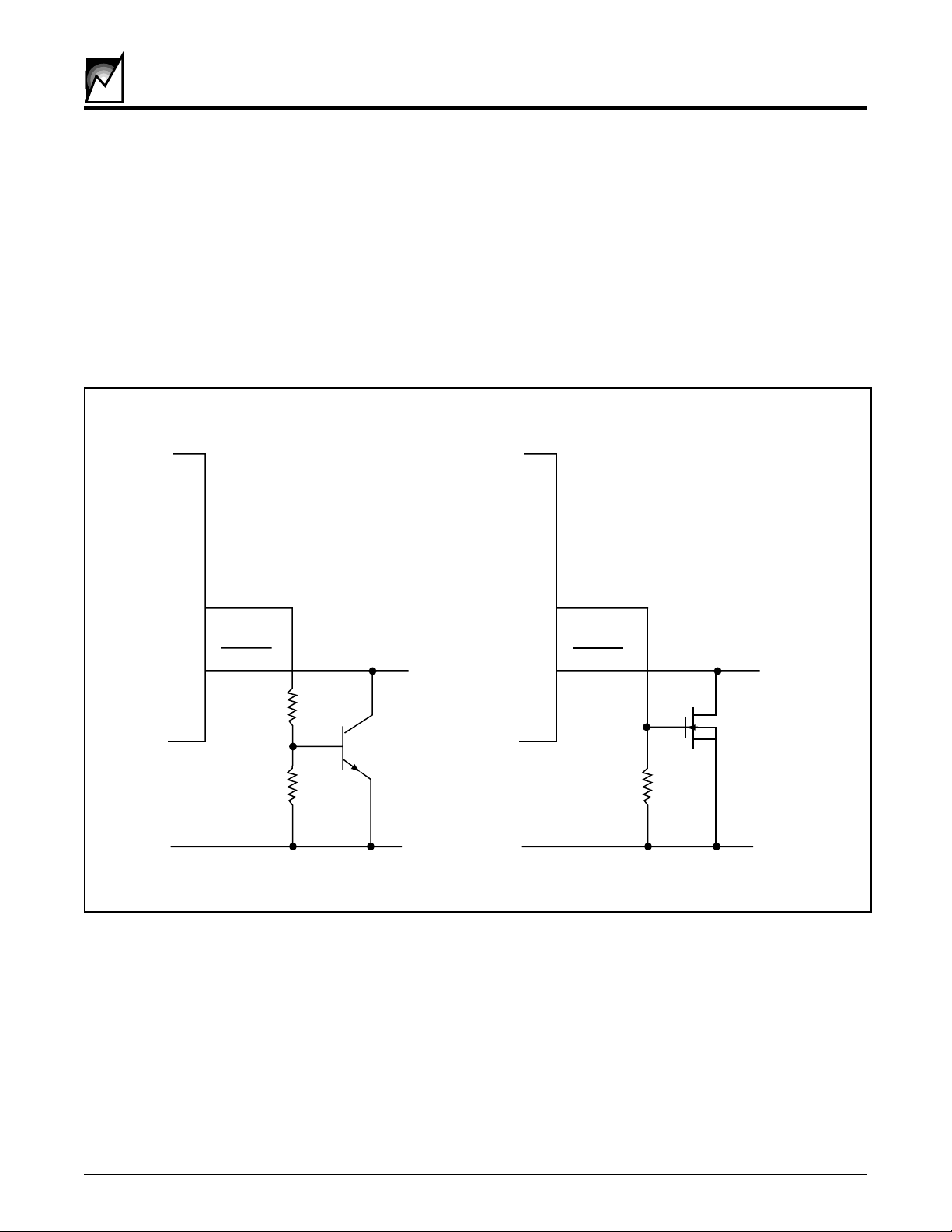
Boosting RESET Output Drive
S39421
The slew-rate of the RESET output is >30V/µs at the LO
to HI logic transition with a 50pF load and a 1.5ký pull-up
resistor. If the RESET output needs to drive a larger load
capacitance or needs to slew faster, then an external NPN
transistor or N-channel MOSFET must be added to boost
S39421 - Circuits to Increase RESET Output Drive
RESET
S39421/4
2N3904
RESET
output current. The RESET output drives the external
transistor providing a current sink capability of >30mA on
the RESET output. Using the boost circuit with a 430ý
pull-up resistor and 100pF load capacitance, the slewrate increases to >50V/µs. See diagrams below.
RESET
S39421/4
TN0200T
RESET
3.9k
10k
GND
Ω
4.7k
Ω
Ω
GND
2024 ILL26.0
FIGURE 21. RESET CURRENT BOOST CIRCUIT
18
2024 9.1 1/23/01
SUMMIT MICROELECTRONICS, Inc.
Page 19
SUMMIT MICROELECTRONICS, Inc.
+3.3V
+5V
+12V
Gnd
Gnd
Gnd
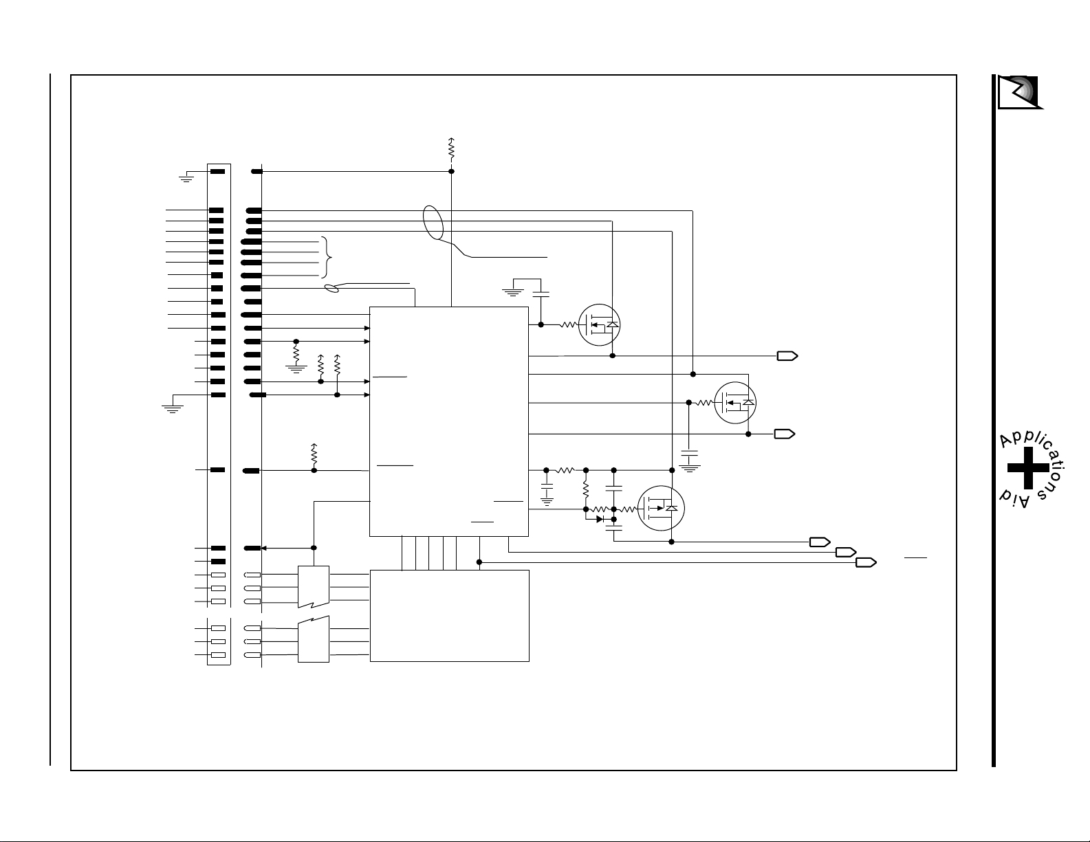
FIGURE 22. TYPICAL INTERFACE SCHEMATIC
2024 9.1 1/23/01
Gnd
+5V
Gnd
PCI_RST#
BD_SEL2#
HEALTHY#
BD_SEL1#
Early & Back End Gnd
Early Power
Switch
GND
VSEL
HST_PWR
HST_RST
PND1
SGNL_VLD
CARD_V_VLD
DD
VCC5 PND2
CS SK DO DI
Back End Power
VGATE5
CARD_5V
3Volt
VGATE3
CARD_3V
VCC12
DRVREN
RESET RESET
47nF
1KΩ
47nF
*
10Ω
G
D
S
Board 5V
*
G
D
10Ω
S
Board 3.3V
47nF
S
10Ω
*
G
D
Board 12V
CARD RESET
CARD RESET
19
Bus
PCI Interface ASIC
* 10 ohm resistors must be located as close as possible to the MOSFETs.
2024 ILL16.7
S39421
Page 20
S39421
VCC5
S39421
Host
Bus 5V
1N4148
1.5kΩ
0.1µF
DRVREN
4.7kΩ
4.7kΩ
330kΩ
1N4148
330kΩ
1N4148
Host
-12V Bus
0.33µF
0.1µF
G
10Ω
*
0.33µF
G
10Ω
*
To Backend -12V
D
N-Channel
Power
S
MOS FET
Host
+12V Bus
S
D
P-Channel
Power
MOS FET
To Backend +12V
20
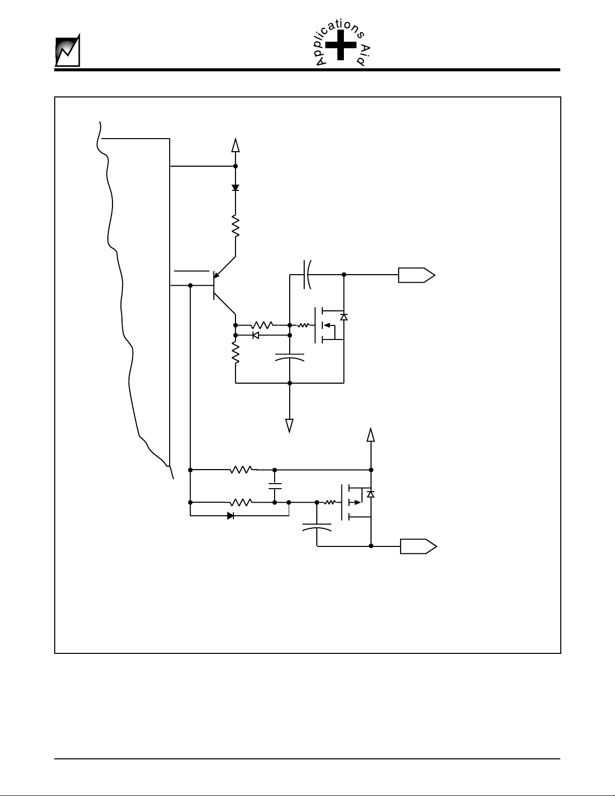
* 10 ohm resistors must be located as close as possible to the MOSFETs.
FIGURE 23. +12V AND -12V CONTROL
2024 9.1 1/23/01
2024 ILL17.5
SUMMIT MICROELECTRONICS, Inc.
Page 21
Using the S39421 as the Primary Control Circuit
on a VME Live Insertion Card
S39421
High availability is a key feature of many types of systems
today. Whether the system is a central office switch, a
private branch exchange or a server it is important the
system stay up and running while adding new services
(add-in cards) or replacing faulty boards. Therefore, a
means for inserting and removing cards while the entire
system is powered-on (live) is a necessity.
Live insertion poses a number of challenges for the addin card designer. For live insertion to be trouble free we
first need to prevent damage to components on the addin card due to improper supply sequencing. Secondly,
voltage drop on the system power busses must be prevented in order to avoid unwanted system reset condition.
Lastly, the integrity of the system’s signals needs to be
maintained when additional circuitry is connected to the
bus.
Based upon the proposed Live Insertion System Requirements the S39421 is an ideal candidate as the add-in
card’s live insertion controller.
Sequencing the Voltages
The proposed live insertion specification (see references)
outlines 26 operational steps during the insertion of a
card. These are broken down into two major categories;
the “Insertion Process” and the “Typical Board Recognition Process.”
The first 6 steps have to do with the insertion of the card
and sequencing the discharge of any voltage potentials
so that by the time the board is ready to make contact with
the backplane no ESD discharges will occur. Even though
the balance of the actions tend to overlap they can be
viewed as two operations: the add-in card/backend logic
sequencing and the backplane/add-in card interface sequencing.
Add-in Card/Backend Logic Sequencing
The process of electrical insertion begins with the contact
of special ground and voltage pins. These are longer than
the signal and power pins and they are physically located
at opposite ends of the connector. The voltage pins are
labeled Vpc (pre-charge Voltage), this is the backplane’s
5 volt supply and the intent is for this voltage to be used
to power the sequencing circuitry, any ASICs that interface to the bus and to pre-charge the ‘bus-side’ lines of the
signal transceivers.
The PC board should be laid out so that ground is routed
to all circuits, i.e. grounds should not be linked via the PCB
connector. Vpc should be tied directly to the VCC5 pin on
the S39421 and the device will immediately begin driving
its backend circuit control signals [SGNL_VLD,
CARD_V_VLD, RESET and RESET] and it will place the
voltage ramp control signals [VGATE3, VGATE5 and
DRVREN] in the off state.
The next step is for the controller to recognize that the
board is properly seated in the connector. VME has an
optional feature that lends itself ideally to this step of the
operation; the ejector handles can be used to activate a
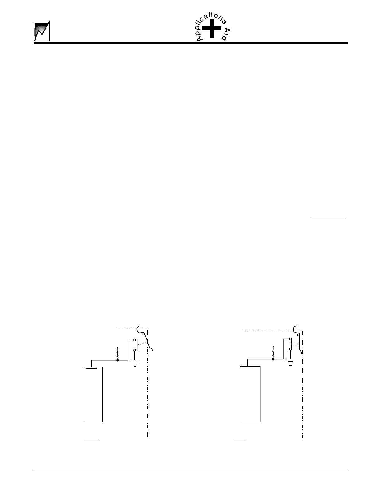
switch when they are fully rotated and locked. Switch
closure can be used as the PND1 and PND2 inputs on the
S39421. The pull-up resistor used for this implementation
must be tied to Vpc because the backend voltages will not
yet have been switched on by the S39421.
PND1
S39421
Ejector and Switch Open
PND1 Pulled High
FIGURE 24: ILLUSTRATION OF CARD INJECTOR/EJECTOR SWITCH CIRCUIT
SUMMIT MICROELECTRONICS, Inc.
Vpc
2024 9.1 1/23/01
Vpc
PND1
S39421
Card Seated Ejector Locked
and PND1 Driven to Gnd
2024 ILL27.0
21
Page 22
S39421
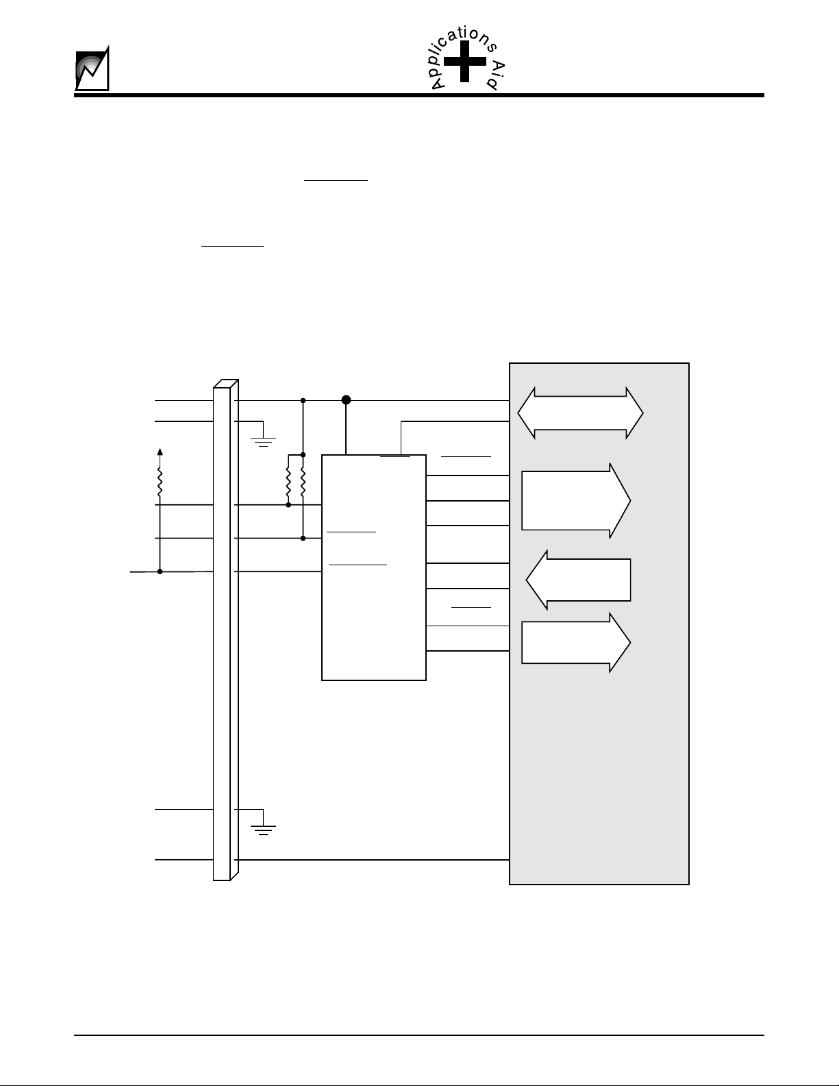
The board’s pins should now be mated with the backplane
connector which in turn will bring the host LI/I* and
RESET* signals to the S39421. These signals should be
tied to the device’s HST_PWR and HST_RST inputs
respectively. Whenever HST_PWR is low the outputs
controlling the backend power on sequencing will be
inhibited; it does not impact the reset outputs or reset
timer. When low, the HST_RST input will force the reset
outputs active; once it is released the reset timer will be
started and it will keep the reset outputs active for t
Vpc
Gnd
System
Vcc
IL/I*
RESET*
LI/O*
VCC5
HST_PWR
HST_RST
SGNL_VLD
PURST
PND1
S39421
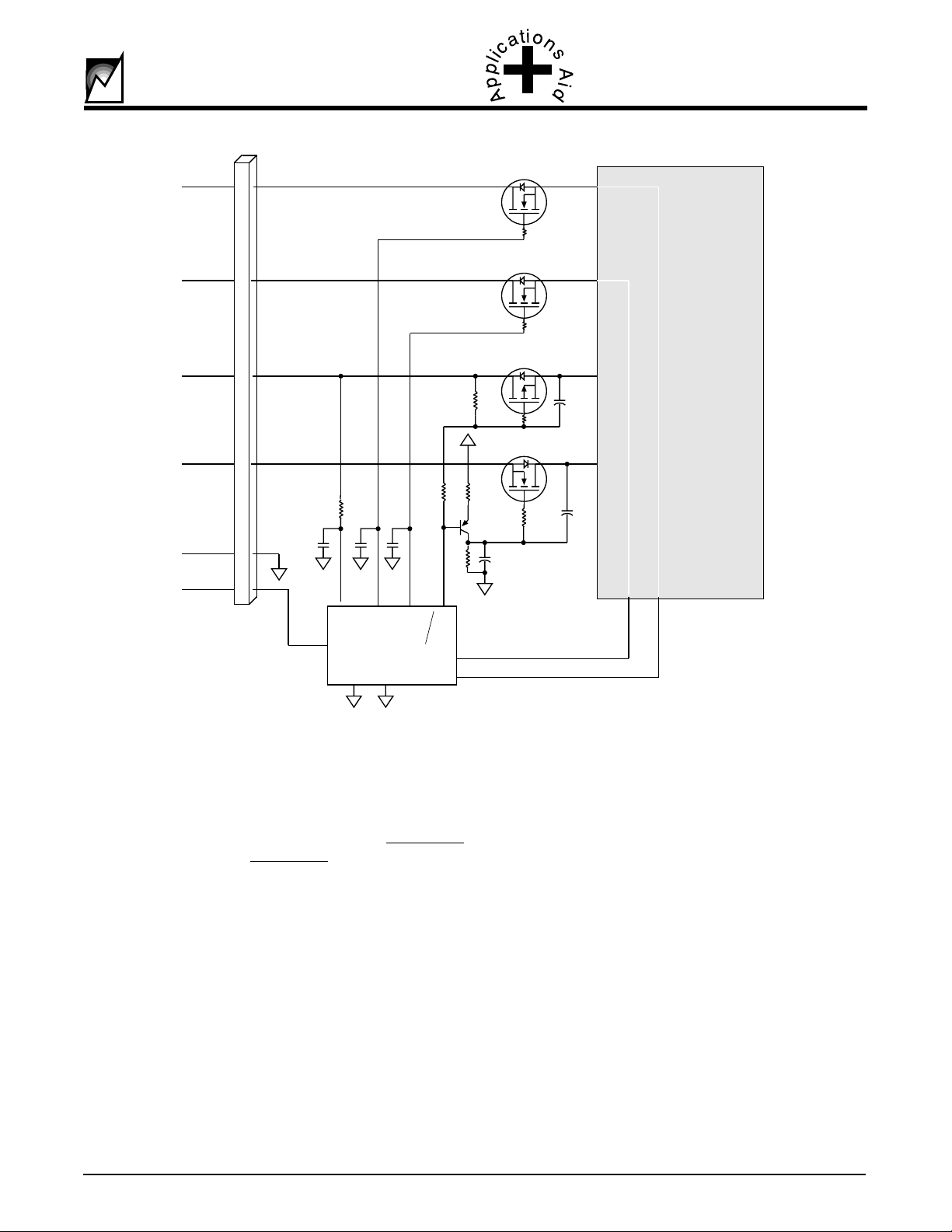
At the same time the signal pins are making contact, the
backend voltages are applied to the card (3.3V, 5V, +12V
and -12V on short pins), but, they are blocked by FETs
under the control of the S39421 (see figure 3 ). Depending
upon the state of the VSEL pin, the S39421 will monitor
either the bussed +5V only, the bussed +3.3V only or both
the bussed +5V and +3.3V. Once the S39421 has determined these supply voltages are at or above Vtrip, (and LI/
I* has released HST_PWR) it will release the VGATE
.
outputs and effectively turn them on at a rate equivalent
to 250V/second. At the same time it will force DRVREN
active thus providing power to the backend circuits.
Ejector Switch
Circuit
DRVREN
VGATE3
VGATE5
CARD3V
CARD5V
RESET
RESET
Backend
Power Circuits
See Figure
Backend V oltage
to S39421
Monitor Circuits
Reset Control
of Backend
Circuits
Gnd
Vpc
2024 ILL28.0
FIGURE 25: GENERAL BLOCK DIAGRAM OF S39421 HOST BUS INTERFACE AND BACKEND SIGNAL INTERFACE
22
2024 9.1 1/23/01
SUMMIT MICROELECTRONICS, Inc.
Page 23
S39421
Gnd
Vpc
+5V
+3.3V
+12V
-12V
+5V
+3.3V
+12V
-12V
Vpc
Backend Circuitry
Gnd
VCC12
VGATE5
VGATE3
VSEL
DRVREN
CARD_3V
CARD_5V
VCC5
S39421
ISLEW
FIGURE 26: BACKEND VOLTAGE CONTROL CIRCUIT
The S39421 will now begin monitoring the backend circuit
voltages and when they are at or above Vtrip the reset
timer will be released to begin the time out period and
CARD_V_VLD will be released. After tPURST has expired, the reset outputs will be released and SGNL_VLD
will be driven active. The SGNL_VLD signal can be tied to
the host LI/O* signal pin to indicate the card has been fully
powered, cleanly reset and is ready for action.
Backplane/Add-in Card Sequencing
A more complicated problem than the sequencing shown
above is the signal bus interface. Inserting unpowered
circuits onto the signal bus could lead to a situation of
damaging components and much more likely disrupting
the signals on the backplane. This will involve a rigorous
evaluation and selection process by the design engineer
to determine the best solution for the individual application. However, we can examine a product family that
should resolve most of the issues the designer might
encounter. The proposed VME Live Insertion spec actu-
2024 ILL29.3
ally helps us narrow this down quickly by recommending
the use of ABTE logic. This is available from at least two
large manufacturers of semiconductors.
Avoidance of Bus Conflicts
Bus conflicts arise when two or more interface circuits
attempt to drive the bus simultaneously with one circuit
driving high and the other driving low. The device trying to
drive low will most likely not incur damage. But the device
trying to drive high will be dropping 5Volts on its output at
up to 120mA current. Even for very short periods of time
the high temperatures this will generate can either destroy
the device or adversely affect the long-term reliability of
the device. The best solution is to insure the transceiver’s
enable input is actively driven before the transceiver is
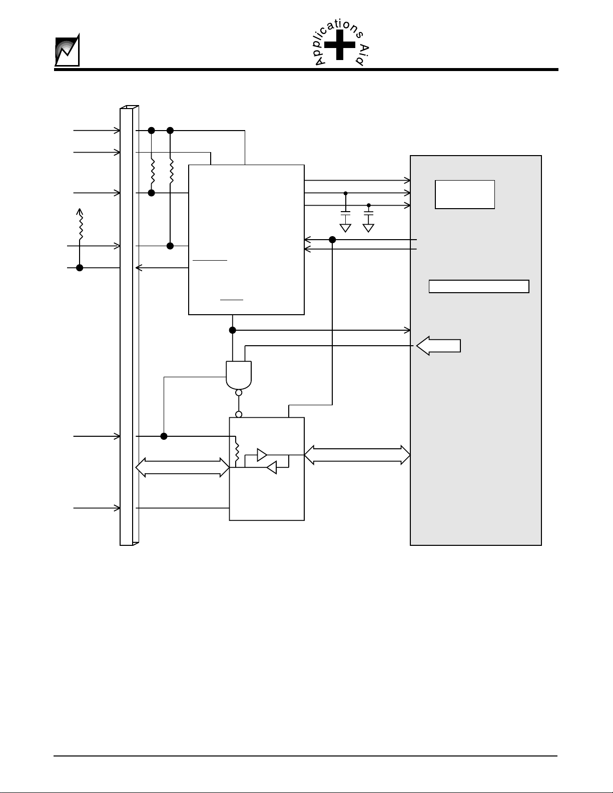
powered-on. Using one of the reset outputs (as shown in
figure 27) as a gating signal to a single enable input style
transceiver is one solution. With a dual enable transceiver
one of the reset outputs can be tied directly to appropriate
enable input.
SUMMIT MICROELECTRONICS, Inc.
2024 9.1 1/23/01
23
Page 24

S39421
Pre-bias
The switching capacitance of the individual signal lines at
the interface must be charged to the instantaneous voltage on the corresponding bus line. These currents distort
the signal that is being transmitted at that instant. To
address this issue the proposed VME Live Insertion Spec
states: “All VME system drivers and receivers SHALL be
pre-biased to 1.7 =/-0.2 Vdc with a resistive network
powered by the pre-charge +5V. . . before the board signal
pins contact the backplane VME64 bus connector(s).”
The ABTE logic addresses this issue head-on by providing a separate VCCBias pin that is internally connected to
a pre-charge resistor network.
CARD REMOVAL
A clean transition for card removal can be performed
either by the opening of the injector/ejector levers which
in turn opens the switches that force the PND inputs to
ground or by the host driving LI/I* low. Both actions will tell
the S39421 to disable the high side drivers and force the
reset outputs active.
RECAP
As the board is first inserted into the backplane voltage
potentials on are shunted to ground thru the use of various
bleed resistors and physical contact with the chassis
frame. These are make then break processes so that by
the time the card is ready to make contact with the
backplane connector the board is electrically isolated
from the frame.
The first pins of the connector to make contact with the
backplane are ground and Vpc (pre-charge VCC). Vpc
should be tied directly to the S39421 and the transceiver
BiasVcc input. Once the S39421 detects the presence of
Vpc it will begin driving the reset outputs active, shut off all
the control signals to the power FETs and begin driving
the LI/O* low. The injector/ejector levers will close the
switches grounding the PND inputs allowing the S39421
to check the state of the VSEL pin and determine what bus
voltages should be monitored. If the bus voltages are at
or greater than Vtrip AND LI/I* has been released the
S39421 will turn on the high side driver outputs VGATE3
and VGATE5 and the DRVREN output.
The voltages to the backend logic are applied with a
nominal slew rate of VGATE3 and VGATE5 set at 250V/
sec. The backend voltages should also be fed back to the
S39421 and as soon as they are at or above their Vtrip
level, the CARD_V_VLD will be released. If the host has
released its RESET input and LI/I* input, the S39421 will
release the timer for its reset circuit. After tPURST the
reset outputs to the backend logic will be released and the
SGNL_VLD output will be driven active [backplane signal
LI/O]. This is the final step in activating a board for live
insertion.
24
2024 9.1 1/23/01
SUMMIT MICROELECTRONICS, Inc.
Page 25
Vpc
Gnd
LI/O*
LI/I*
d-1
d-2
HST_RST
HST_PWR
SGNL_VLD
S39421
RESET
S39421
Vcc5Gnd
DRVREN
VGATE3
VGATE5
CARD_5V
CARD_3V
To Add-in Card
Back-end V oltage
Ramp Circuits
Add-in Card Backend Circuitry
CARD-OE
Vpc
Gnd
d-32
d-31
VccBias
OE
ABTE245
Gnd
Vcc
FIGURE 27: A BUS INTERFACE SOLUTION
2024 ILL30.1
SUMMIT MICROELECTRONICS, Inc.
2024 9.1 1/23/01
25
Page 26

Appendix A
MOSFETs suitable for use with the S39421 Hot-Swap Controller
N-Channel MOSFETs
S39421
Part Number Manufacturer V(BR)
DSS
R
DS(on)
@ VGS=10V ID cont. Package
IRF7603 Int. Rectifier 30V 35 milliohms max 4.5A Micro-8
IRF7413 Int. Rectifier 30V 11 milliohms max 9.2A SO-8
MTSF3N03HD Motorola 30V 40 milliohms max 3A Micro-8
MMSF7N03HD Motorola 30V 28 milliohms max 8A SO-8
MTD20N03HDL2 Motorola 30V 35 milliohms max 20A DPAK
Si6434DQ Temic 30V 28 milliohms max 5.6A TSSOP-8
Si6410DQ Temic 30V 14 milliohms max 7.8A TSSOP-8
Si4412DY Temic 30V 28 milliohms max 7A SO-8
Si4416DY Temic 30V 18 milliohms max 9A SO-8
P-Channel MOSFETs
Part Number Manufacturer V(BR)
DSS
R
DS(on)
@ VGS=10V ID cont. Package
IRF7606 Int. Rectifier -30V 90 milliohms max 2.9A Micro-8
IRF7416 Int. Rectifier -30V 20 milliohms max 7.1A SO-8
MTSF2P03HD Motorola -30V 90 milliohms max 2.4A Micro-8
MMSF3P02HD Motorola -20V 75 milliohms max 3A SO-8
MTD20P03HDL2 Motorola -30V 99 milliohms max 19A DPAK
Si6435DQ Temic -30V 90 milliohms max 4.5A TSSOP-8
Si6415DQ Temic -30V 19 milliohms max 6.5A TSSOP-8
Si4431DY Temic -30V 40 milliohms max 5.8A SO-8
Si4435DY Temic -30V 20 milliohms max 8A SO-8
References:
VITA Standards Organization, November 1997,
VME64x Live Insertion System Requirements Draft Standard
Summit Microelectronics, Inc. S39421 Data Sheet
Texas Instruments Application Note SDYA012, October 1996,
26
2024 9.1 1/23/01
Live Insertion
SUMMIT MICROELECTRONICS, Inc.
Page 27
Ref. JEDEC MS-013
Inches
(Millimeters)
0.291 - 0.299
(7.40 - 7.60)
0.010 - 0.029
(0.25 - 0.75)
×45º
0 to 8
0 to 8
typ
typ
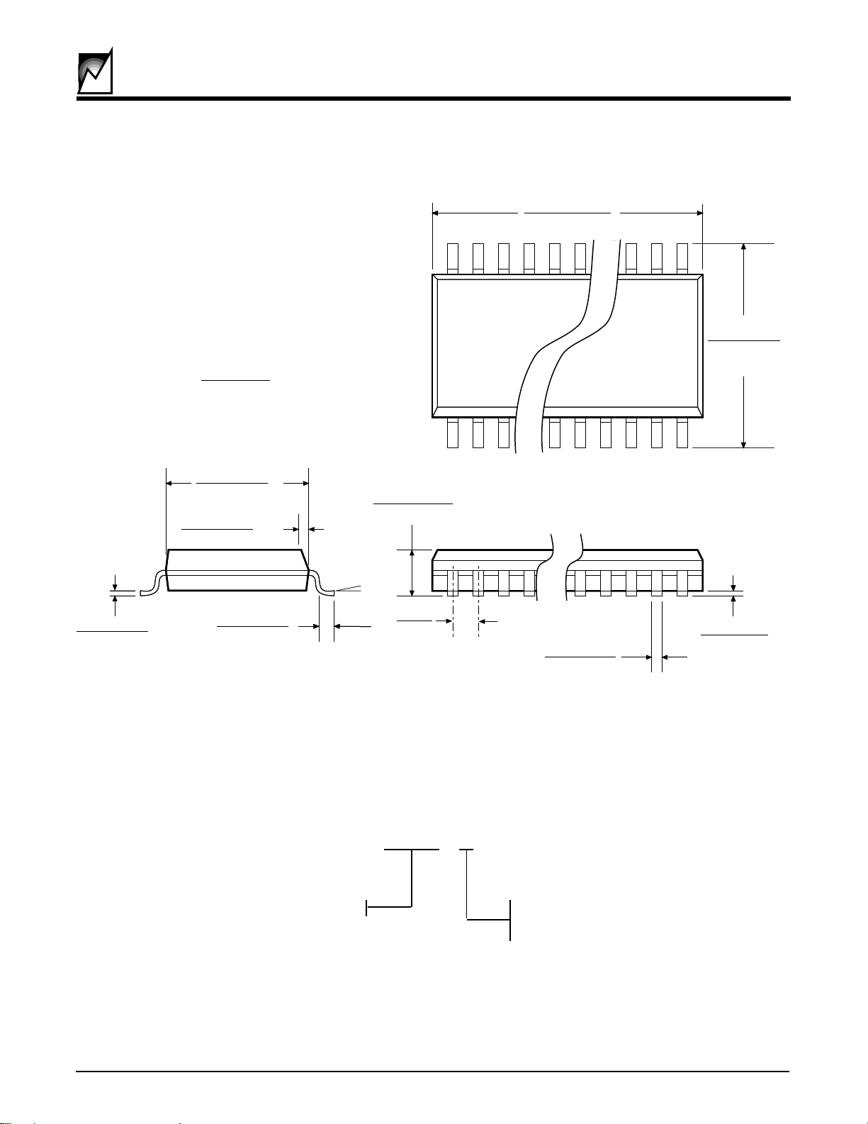
24 Pin SOIC
1
0.093 - 0.104
(2.35 - 2.65)
5
0.697 - 0.614
(15.20 - 15.60)
S39421
0.394 - 0.419
(10.00 - 10.65)
0.009 - 0.013
(0.23 - 0.32)
0.016 - 0.050
0.016 - 0.050
(0.40 - 1.27)
ORDERING INFORMATION
Base Part Number
0.05
(1.27)
S39421
0.004 - 0.012
0.013 - 0.020
(0.33 - 0.51)
(0.10 - 0.30)
24 Pin SOIC
S
Package
S = 24 Lead SOIC
2024 ILL18.0
SUMMIT MICROELECTRONICS, Inc.
2024 9.1 1/23/01
27
Page 28

S39421
NOTICE
SUMMIT Microelectronics, Inc. reserves the right to make changes to the products contained in this publication
in order to improve design, performance or reliability. SUMMIT Microelectronics, Inc. assumes no responsibility
for the use of any circuits described herein, conveys no license under any patent or other right, and makes no
representation that the circuits are free of patent infringement. Charts and schedules contained herein reflect
representative operating parameters, and may vary depending upon a user’s specific application. While the
information in this publication has been carefully checked, SUMMIT Microelectronics, Inc. shall not be liable for any
damages arising as a result of any error or omission.
SUMMIT Microelectronics, Inc. does not recommend the use of any of its products in life support or aviation
applications where the failure or malfunction of the product can reasonably be expected to cause any failure of
either system or to significantly affect their safety or effectiveness. Products are not authorized for use in such
applications unless SUMMIT Microelectronics, Inc. receives written assurances, to its satisfaction, that: (a) the risk
of injury or damage has been minimized; (b) the user assumes all such risks; and (c) potential liability of SUMMIT
Microelectronics, Inc. is adequately protected under the circumstances.
© Copyright 2001 SUMMIT Microelectronics, Inc.
This Document supersedes all previous versions.
28
2024 9.1 1/23/01
SUMMIT MICROELECTRONICS, Inc.
 Loading...