

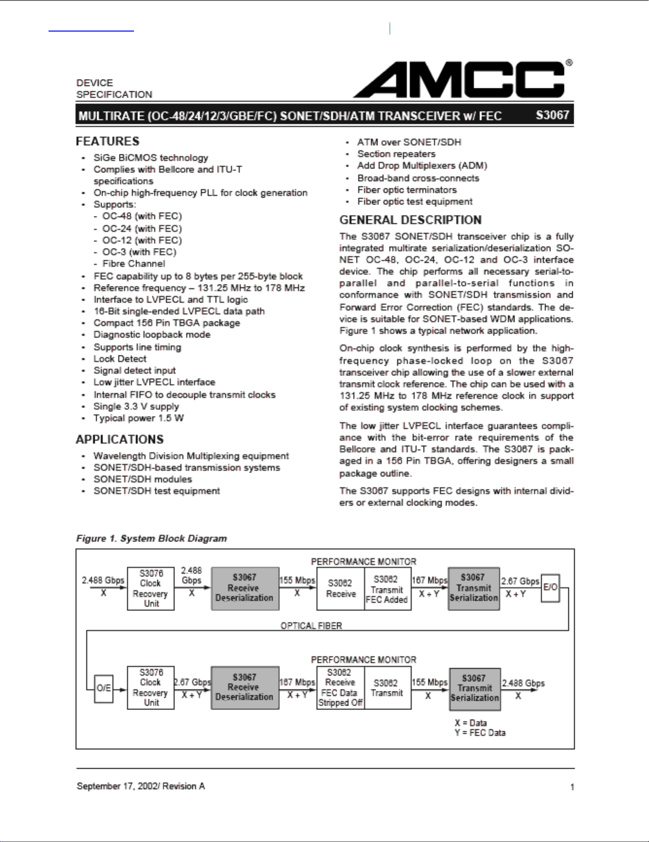
Page 1
查询S3062供应商
Page 2
Page 3
3
S3067MULTIRATE (OC-48/24/12/3/GBE/FC) SONET/SDH/ATM TRANSCEIVER w/ FEC
September 17, 2002/ Revision A
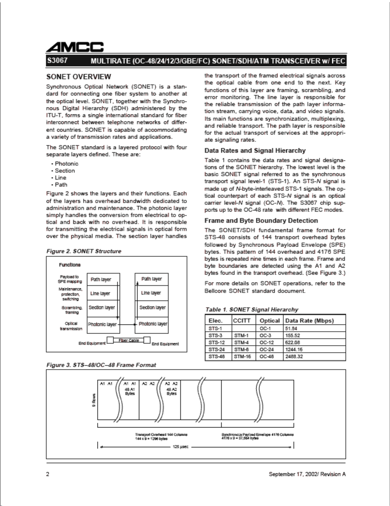
S3067 OVERVIEW
The S3067 transceiver implements SONET/SDH
and WDM serialization/deserialization, and transmission functions. The block diagram in Figure 4 shows
the basic operation of the chip. This chip can be
used to implement the front end of WDM equipment,
which consists primarily of the serial transmit interface and the serial receive interface. The chip
handles all the functions of these two elements, including parallel-to-serial and serial-to-parallel
conversion, clock generation, and system timing.
The system timing circuitry consists of management
of the data stream and clock distribution throughout
the front end.
S3067 has the ability to bypass the internal VCO
with an external source and also with the receive
clock. The device generates 14/15, 15/14, 16/17 and
17/16 clocks based upon the received clock and an
external clock to incorporate the FEC capability. The
dividers support the first two rates shown in Table 4.
The S3067 is divided into a transmitter section and a
receiver section. The sequence of operations is as
follows:
0LESETAR1LESETARedoMgnitarepO
00 3-CO
01 21-CO
10 CF/EBG/42-CO
11 84-CO
Table 2. Data Rate Select
Transmitter Operations:
1. 16-bit parallel input
2. Parallel-to-serial conversion
3. Serial output
Receiver Operations:
1. Serial input
2. Serial-to-parallel conversion
3. 16-bit parallel output
Internal clocking and control functions are transparent to the user. S3067 Supports six different code
rates, besides the normal rate, for each of the four
operating modes.
ytilibapaCgnitcerroCrorrE
gniwohsetaRedoC
eudnoisnapxEhtdiwdnaB
BSF&sdrowedocot
kcolctupnidesaercnifoelpmaxE
)zHM(61-MTS/84-STSrofycneuqerf
kcolbetyb-552repsetyb8esaercni%41.7=832/552 36.661=41/51*25.551=832/552*25.551
kcolbetyb-552repsetyb7esaercni%52.6=042/552 42.561=61/71*25.551=042/552*25.551
kcolbetyb-552repsetyb6esaercni%73.5=242/55278.361=242/552*25.551
kcolbetyb-552repsetyb5esaercni%15.4=442/55235.261=442/552*25.551
kcolbetyb-552repsetyb4esaercni%66.3=642/552 12.161=28/58*25.551=642/552*25.551
kcolbetyb-552repsetyb3esaercni%28.2=842/55219.951=842/552*25.551
Table 4. FEC Modes
Table 3. FEC Select
0CEF12
OCV
rediviD
KLCSR
rediviD
001 7161
101 6171
011 5141
111 4151
000 71X
100 61X
010 51X
110 41X
CCMA6703SeciveDyrevoceRkcolC84-CO
CCMA2603SrotinoMecnamrofreP84-CO
Suggested Interface Devices
Page 4
4
S3067
MULTIRATE (OC-48/24/12/3/GBE/FC) SONET/SDH/ATM TRANSCEIVER w/ FEC
September 17, 2002/ Revision A
Figure 4. S3067 Transceiver Functional Block Diagram
CLOCKS
LOCKDET
155MCKP/N
19MCK
PCLKP/N
PHERR
TSDP/N
TSCLKP/N
OVREF
POUT[15:0]
POCLKP/N
TIMGEN
16:1
PARALLEL
TO SERIAL
CLOCK
SYNTHESIZER
D
TXDP/N
TXCLKP/N
POCLK (Internal)
REFCLKP/N
PICLKP/N
TXDP/N
(Internal)
TXCLKP/N
(Internal)
RSCLKP/N
DLEB
SQUELCH
IVREF
RSTB
SDLVPECL
SDTTL
RSDP/N
KILLRXCLK
LLEB
PIN[15:0]
BYPASS
TESTEN
CAP2
CAP1
RLPTIME
FECSEL2
PHINIT
D
D
D
1:16
SERIAL TO
PARALLEL
TIMGEN
R
3
16
16
RATESEL[0:1]
FECSEL[2:0]
BYPASSCLKP/N
N
SLPTIME
VCO CLOCK
TX
RX
2
Page 5

5
S3067MULTIRATE (OC-48/24/12/3/GBE/FC) SONET/SDH/ATM TRANSCEIVER w/ FEC
September 17, 2002/ Revision A
Figure 5. Clock Synthesizer
M
N
PD
LPF
VCO
VCOCLK
REFCLK
FECSEL (0-1)
FECSEL 2
RSCLK
Where N = 14/15/16/17
M = 14/15/16/17
RSCLK N
VCOCLK M
RSCLK Divider
VCO Divider
=
A high on FECSEL2 selects RSCLK divided by N. A
low on FECSEL2 selects the REFCLK. The REFCLK
or RSCLK divided by N is divided by 1/M (multiplied
by M) in the loop. The value of M and N can be
selected by FECSEL0 and FECSEL1.
When FECSEL2 = 0, VCOCLK = REFCLK * M. The
user must select the proper value of REFCLK and M
to get the desired VCOCLK frequency. When
FECSEL2 = 1, VCOCLK = (RSCLK * M) ÷ N. The
user must select the proper M/N ratio (with
FECSEL0 and FECSEL1) to get the desired
VCOCLK value. (See Tables 3 and 4.)
Example: OC-48 FEC capability of 8 bytes per
255-byte block. Required VCOCLK = 2.6656 GHz.
Method 1:
Required VCOCLK = 2.6656 GHz
FECSEL2 = 0, selects REFCLK
FECSEL0 = 1 and FECSEL1 = 0, selects VCO
divider(M) = 16
REFCLK = 2.6656 GHz ÷ 16 = 166.60 MHz
VCOCLK = REFCLK ÷ (1/M) = 166.60 * 16 = 2.6656
GHz
Method 2:
Required VCOCLK = 2.6656 GHz
FECSEL2 = 1, selects RSCLK
FECSEL0 = 0 and FECSEL1 = 0, selects VCO
divider(M) = 17 and RSCLK divider(N) = 16
RSCLK = (2.6656 * 16) ÷ 17 = 2.5088 GHz
VCOCLK = RSCLK ÷ N ÷ (1/M) = 2.5088 GHz ÷ 16 *
17 = 2.6656 GHz.
Page 6
6
S3067
MULTIRATE (OC-48/24/12/3/GBE/FC) SONET/SDH/ATM TRANSCEIVER w/ FEC
September 17, 2002/ Revision A
S3067 TRANSCEIVER
FUNCTIONAL DESCRIPTION
Transmitter Operation
The S3067 transceiver chip performs the serialization
stage in the processing of a transmit SONET STS-48/
STS-24/STS-12/STS-3/GBE/FC data stream depending on the data rate selected. It converts 16-bit
parallel data to bit serial format.
A high-frequency bit clock can be generated from a
131.25 MHz to 178 MHz frequency reference by using an integral frequency synthesizer consisting of a
phase-locked loop circuit with a divider in the loop.
Diagnostic loopback (transmitter to receiver) and line
loopback (receiver to transmitter) is provided. See
Other Operating Modes
.
The bypass signal selects between the BYPASSCLK
and the VCO clock. BYPASSCLK can be used to provide an alternative clock to the internal VCO when the
user selects an error correcting capability which is not
provided by the S3067 dividers. The user must provide the required frequency for the BYPASSCLK
when error-correcting capability of 6/5/4/3 bytes per
255-byte block is selected.
Clock Synthesizer
The clock synthesizer, shown in the block diagrams
of Figures 4 and 5, is a monolithic PLL that generates the serial output clock frequency locked to the
input Reference Clock (REFCLKP/N).
The REFCLKP/N input must be generated from a
crystal oscillator that has a frequency accuracy better than the value stated in Table 10 in order for the
TSCLK frequency to have the accuracy required for
operation in a SONET system. Lower-accuracy crystal oscillators may be used in applications less
demanding than SONET/SDH.
The on-chip PLL consists of a phase detector, which
compares the phase relationship between the VCO
output and the REFCLKP/N input, a loop filter which
converts the phase detector output into a smooth DC
voltage, and a VCO, whose frequency is varied by
this voltage.
The divide by ‘N’ and divide by ‘M’ provide the
counters required to support error correcting capability. The values of ‘N’ and ‘M’ can be selected by
FECSEL lines.
The loop filter generates a VCO control voltage
based on the average DC level of the phase discriminator output pulses. A single external clean-up
capacitor is utilized as part of the loop filter. The loop
filter’s corner frequency is optimized to minimize output phase jitter.
Timing Generator
The timing generation function, seen in Figure 4,
provides a divide-by-16 version of the transmit serial
clock. This circuitry also provides an internally generated load signal, which transfers the PIN[15:0]
data from the parallel input register to the serial shift
register.
The PCLK output is a divide-by-16 rate version of
transmit serial clock (divide-by-16). PCLK is intended for use as a divide-by-16 clock for upstream
multiplexing and overhead processing circuits. Using
PCLK for upstream circuits will ensure a stable frequency and phase relationship between the data
coming into and leaving the S3067 device.
The timing generator also produces a feedback reference clock to the clock synthesizer. A counter
divides the synthesized clock down to the same frequency as the reference clock REFCLK. The PLL in
the clock synthesizer maintains the stability of the
synthesized clock by comparing the phase of the
internal clock with that of the Reference Clock
(REFCLK).
Table 5. Reference Jitter Limits
edoMgnitarepOhtdiWdnaBrettiJSMR
84-STSzHM02otzHk21cBd1642-STSzHM01otzHk21sp2
21-STSzHM5otzHk21sp4
3-STSzHM1otzHk21sp61
Page 7

7
S3067MULTIRATE (OC-48/24/12/3/GBE/FC) SONET/SDH/ATM TRANSCEIVER w/ FEC
September 17, 2002/ Revision A
Parallel-to-Serial Converter
The parallel-to-serial converter shown in Figure 4 is
comprised of a FIFO and a parallel-to-serial register.
The FIFO input latches the data from the PIN[15:0]
bus on the rising edge of PICLK. The parallel-toserial register is a loadable shift register which takes
its parallel input from the FIFO output.
An internally generated divide-by-16 clock, which is
phase aligned to the transmit serial clock as described in the
Timing Generator
description, activates
the parallel data transfer between registers. The serial
data is shifted out of the parallel-to-serial register at
the TSCLK rate
.
FIFO
A FIFO is added to decouple the internal and external (PICLK) clocks. The internally generated
divide-by-16 clock is used to clock out data from the
FIFO. PHINIT and LOCKDET are used to center or
reset the FIFO. The PHINIT and LOCKDET signals
will center the FIFO after the third PICLK pulse. This
is to insure that PICLK is stable. This scheme allows
the user to have an infinite PCLK-to-PICLK delay
through the ASIC. Once the FIFO is centered, the
PCLK-to-PICLK delay can have a maximum drift as
specified in Table 20.
FIFO Initialization
The FIFO can be initialized in one of the following
three ways:
1. During power up, once the PLL has locked to
the reference clock provided on the REFCLK
pins, the LOCKDET will go active and initialize
the FIFO.
2. When RSTB goes active, the entire chip is reset.
This causes the PLL to go out of lock and thus
the LOCKDET goes inactive. When the PLL reacquires the lock, the LOCKDET goes active
and initializes the FIFO. Note: PCLK is held reset when RSTB is active.
3. The user can also initialize the FIFO by raising
PHINIT.
During the normal running operation, the incoming
data is passed from the PICLK timing domain to the
internally generated, divide-by-16 clock timing domain. Although the frequency of PICLK and the
internally generated clock is the same, their phase
relationship is arbitrary. To prevent errors caused by
short setup or hold times between the two timing
domains, the timing generator circuitry monitors the
phase relationship between PICLK and the internally
generated clock. When a potential setup or hold time
violation is detected, the phase error goes high.
When PHERR conditions occur, PHINIT should be
activated to recenter the FIFO (at least 2 PCLK periods). This can be done by connecting PHERR to
PHINIT. When realignment occurs, up to 10 bytes of
data will be lost. The user can also take in the
PHERR signal, process it and send an output to
PHINIT in such a way that idle bytes are lost during
the realignment process. PHERR will go inactive
when the realignment is complete.
Receiver Operation
The S3067 receiver chip provides the first stage of
digital processing of a receive SONET STS-48/STS24/STS-12/STS-3/GBE/FC bit-serial stream. The
bit-serial data stream is then converted into a 16-bit
half-word data format. A loopback mode is provided
for diagnostic loopback (transmitter to receiver). A line
loopback (receiver to transmitter) is also provided.
Both line and local loopback modes can be active at
the same time.
Serial-to-Parallel Converter
The serial-to-parallel converter consists of two 16-bit
registers. The first is a serial-in, parallel-out shift register, which performs the serial-to-parallel conversion
clocked by the clock recovery block. On the falling
edge of the POCLK, the data in the parallel register
is transferred to an output parallel register which
drives POUT[15:0].
OTHER OPERATING MODES
Diagnostic Loopback
When the Diagnostic Loopback Enable (DLEB) input
is low, a loopback from the transmitter to the receiver at the serial data rate can be set up for
diagnostic purposes. The differential serial output
data from the transmitter is routed to the serial-toparallel block in place of the normal data stream
(RSD). TSD/TSCLK outputs are active. DLEB takes
precedence over SDPECL and SDTTL.
Page 8

8
S3067
MULTIRATE (OC-48/24/12/3/GBE/FC) SONET/SDH/ATM TRANSCEIVER w/ FEC
September 17, 2002/ Revision A
Line Loopback
The line loopback circuitry selects the source of the
data and clock which is output on TSD and TSCLK.
When the Line Loopback Enable input (LLEB) is
high, it selects data and clock from the parallel-toserial converter block. When LLEB is low, it forces
the output data multiplexer to select the data and
clock from the RSD and RSCLK inputs, and a receive-to-transmit loopback can be established at the
serial data rate. Diagnostic loopback and line
loopback can be active at the same time.
Loop Timing
In Serial Loop Timing mode (SLPTIME), the clock
synthesizer PLL of the S3067 is bypassed, and the
timing of the entire transmitter section is controlled
by the Receive Serial Clock, RSCLKP/N. This mode
is entered by setting the SLPTIME input to a TTL
high level.
In this mode, the REFCLKP/N input is not used, and
the RATESEL input is ignored for all transmit functions. It should be carefully noted that the internal
PLL continues to operate in this mode and continues
as the source for the 19MCK and 155MCK. Therefore these signals are being used (e.g. as the
reference for an external S3076 clock recovery device), the REFCLKP/N and RATESEL inputs must
be properly driven.
In Reference Loop Timing mode (RLPTIME), the
Parallel Clock from the receiver (POCLK) is used as
the reference clock to the transmitter. In this mode,
the REFCLKP/N input is not used. The 19MCK and
155MCK are generated from the POCLK in this operating mode. When operating the S3067 in
RLPTIME mode, the 19MCK and 155MCK outputs
should not be used as the back-up reference clock
for a clock and data recovery device (S3066,
S3040). When performing loopback testing (DLEB),
the S3067 must not be in RLPTIME.
Squelched Clock
Operation
Some integrated optical receiver/clock recovery
modules force their recovered serial receive clock
output to the logic zero state if the optical signal is
removed or reduced below a fixed threshold. This
condition is accompanied by the expected
deassertion of the Signal Detect (SD) output.
The S3067 has been designed for operation with
clock recovery devices that provide continuous serial
clock for seamless downstream clocking in the event
of optical signal loss.
For operation with an optical transceiver that provides the
Squelched Clock
behavior as described
above, the S3067 can be operated in the
Squelched
Clock
mode by activating the SQUELCH pin.
In this condition, the Receive Serial Clock (RSCLKP/N)
is used for all receiver timing when the SDLVPECL/
SDTTL inputs are in the active state. When the
SDLVPECL/SDTTL inputs are placed in the inactive
state (usually by the deassertion of LOCKDET or Signal Detect from the optical transceiver/clock recovery
unit), the transmitter serial clock will be used to maintain timing in the receiver section. This will allow the
POCLK to continue to run and the parallel outputs to
flush out the last received characters and then assume
the all-zero state imposed at the serial data input.
It is important to note that in this mode there will be
a one-time shortening or lengthening of the POCLK
cycle, resulting in an apparent phase shift in the
POCLK at the deassertion of the SD condition. Another similar phase shift will occur when the SD
condition is reasserted.
In the normal operating mode, with SQUELCH inactive, there will be no phase discontinuities at the
POCLK output during signal loss or reacquisition
(assuming operation with continuous clocking from
the CRU device such as the AMCC S3076).
Page 9

9
S3067MULTIRATE (OC-48/24/12/3/GBE/FC) SONET/SDH/ATM TRANSCEIVER w/ FEC
September 17, 2002/ Revision A
Table 6. S3067 Transmitter Pin Assignment and Descriptions
emaNniPleveLO/I#niPnoitpircseD
0NIP
1NIP
2NIP
3NIP
4NIP
5NIP
6NIP
7NIP
8NIP
9NIP
01NIP
11NIP
21NIP
31NIP
41NIP
51NIP
elgniS
dednE
LCEPVL
I2A
3B
2B
3C
1A
2C
1B
2D
3E
1C
2E
3F
2F
1E
1F
3G
lellarap,KLCIPehtotdengila,61-yb-edividA.tupnIataDlellaraP
otgnidnopserroc(tibtnacifingistsomehtsi]51[NIP.kcolctupni
ehtsi]0[NIP.)dettimsnarttibtsrifeht,drowMCPhcaefo1tib
,drowMCPhcaefo61tibotgnidnopserroc(tibtnacifingistsael
egdegnisirehtnodelpmassi]0:51[NIP.)dettimsnarttibtsaleht
.KLCIPfo
PKLCIP
NKLCIP
yllanretnI
desaiB
.ffiD
LCEPVL
I4A
3A
elcycytud%05yllanimon,61-yb-edividA.kcolCtupnIlellaraP
otdesusiKLCIP.dengilasi]0:51[NIPhcihwot,kcolctupni
ehtniretsigergnidlohaotnistupniNIPehtnoatadehtrefsnart
selpmasKLCIPfoegdegnisirehT.retrevnoclaires-ot-lellarap
.]0:51[NIP
1PAC
2PAC
golanAI5R
5T
dnaroticapacretlifpoollanretxeehT.roticapaCretliFpooL
.62erugiFeeS.snipesehtotdetcennocerasrotsiser
FERVICDI 4C.egatlovecnerefertupniLCEPVLdedne-elgniS
TINIHPelgniS
dednE
LCEPVL
I2G.gnimitlanretningilaerlliwegdegnisiR.noitazilaitinIesahP
PDST
NDST
.ffiD
LMC
O11R
21R
,slangismaertsatadlairesLMClaitnereffiD.ataDlaireStimsnarT
.eludomrettimsnartlacitponaotdetcennocyllamron
PKLCST
NKLCST
.ffiD
LMC
O8R
9R
desuebnacN/PKLCSTLMClaitnereffiD.kcolClaireStimsnarT
detceleseblliwycneuqerfkcolcsihT.langisDSTehtemiterot
.LESCEFdnaLESETARyb
PKLCP
NKLCP
.ffiD
LCEPVL
O6C
6B
ybkcolctiblanretniehtgnidividybdetarenegkcolcecnereferA
neewtebsrefsnartediw-drowetanidroocotdesuyllamronsitI.61
.ecived7603Sehtdnacigolmaertspu
RREHPelgniS
dednE
LCEPVL
O5AerehthcihwrofelcycKLCPhcaegnirudhgiHsesluP.rorrEesahP
lanretniehtneewtebnoitaloivgnimitdloh/pu-teslaitnetopasi
ehtnodetadpusiRREHP.sniamodgnimitKLCIPdnakcolcetyb
.stuptuoKLCPehtfoegdegnillaf
Page 10

10
S3067
MULTIRATE (OC-48/24/12/3/GBE/FC) SONET/SDH/ATM TRANSCEIVER w/ FEC
September 17, 2002/ Revision A
Table 7. S3067 Receiver Pin Assignment and Descriptions
emaNniPleveLO/I#niPnoitpircseD
PDSR
NDSR
.ffiD
LMC
I51H
51G
yllamronslangismaertsataDlaireSevieceRLMClaitnereffiD
.eludomreviecerlacitponaotdetcennocdnadesaibyllanretnI
.detanimret
LCEPVLDSelgniS
dednE
LCEPVL
I61NevitcA.nwod-lluplanretnihtiwLCEPVL.tceteDlangiSLCEPVL
LCEPVLK01dedne-elgnisA.0cigoltadlehsiLTTDSnehwhgiH
oteludomreviecerlacitpolanretxeehtybnevirdebottupni
siLCEPVLDSnehW.rewoplacitpodeviecerfossolaetacidni
lliwsnip)N/PDSR(nIataDlaireSevieceRehtnoatadeht,evitcani
,evitcasiLCEPVLDSnehW.oreztnatsnocaotdecrofyllanretnieb
nehW.yllamrondessecorpeblliwsnipN/PDSRehtnoatad
daetsnieludomreviecerlacitpoehtotdetcennocebotsiLTTDS
tnemelpmiothgiHdeitebdluohsLCEPVLDSneht,LCEPVLDSfo
natnemelpmiotdetcennocnutfelro,tceteDlangiSwoLevitcana
.tceteDlangiShgiHevitca
LTTDSLTTVLI61PsiLCEPVLDSnehwhgiHevitcA.tceteDlangiSLTTVL
tadlehsiLCEPVLDSnehwwoLevitcA.)0cigol(detcennocnu
lanretxeehtybnevirdebottupniLTTVLdedne-elgnisA.1cigol
lacitpodeviecerfossolaetacidnioteludomreviecerlacitpo
lliwsnipN/PDSRehtnoatadeht,evitcanisiLTTDSnehW.rewop
,evitcasiLTTDSnehW.oreztnatsnocaotdecrofyllanretnieb
.yllamrondessecorpeblliwsnipN/PDSRehtnoatad
PKLCSR
NKLCSR
.ffiD
LMC
I51L
51K
N/PDSRehtroftupnikcolcaylppusotdesU.kcolClaireSevieceR
.detanimretdnadesaibyllanretnI.stupni
0TUOP
1TUOP
2TUOP
3TUOP
4TUOP
5TUOP
6TUOP
7TUOP
8TUOP
9TUOP
01TUOP
11TUOP
21TUOP
31TUOP
41TUOP
51TUOP
elgniS
dednE
LCEPVL
O41F
61E
61D
41E
61C
51D
41D
51C
51B
41A
31C
31A
21C
21B
11C
11B
KLCOPehtotdengila,61ybedivida,subtuptuoatadlellaraP
tibtnacifingistsomehtsi51TUOP.kcolctuptuolellarap
.)deviecertibtsrifeht,drowMCPhcaefo1tibotgnidnopserroc(
ehtnodetadpusi]0:51[TUOP.tibtnacifingistsaelehtsi0TUOP
.KLCOPfoegdegnillaf
PKLCOP
NKLCOP
.ffiD
LCEPVL
O01B
01C
,elcycytud%05yllanimon,61ybedividA.kcolCtuptuOlellaraP
.atadtuptuolairesdrow]0:51[TUOPotdengilasitahtkcolctuptuo
.KLCOPfoegdegnillafehtnodetadpusi]0:51[TUOP
FERVOCDO 41BgniwsdimskcarT.egatlovecnereferLCEPVLdedne-elgniS
.subatadtuptuolellarapfoegatlov
Page 11

11
S3067MULTIRATE (OC-48/24/12/3/GBE/FC) SONET/SDH/ATM TRANSCEIVER w/ FEC
September 17, 2002/ Revision A
Table 8. S3067 Common Pin Assignment and Descriptions
emaNniPleveLO/I#niPnoitpircseD
HCLEUQSLTTVLI61RevitcasiHCLEUQSnehW.hgiHevitcA.hcleuqSkcolCKLCSR
ehtfoecalpnidesueblliwkcolctimsnarteht,evitcanisiDSdna
.KLCSR
PKLCFER
NKLCFER
yllanretnI
desaiB
.ffiD
LCEPVL
I2M
3L
tiblanretniehtrofecnereferehtsadesU.tupnIkcolCecnerefeR
.rezisehtnysycneuqerfkcolc
BELDLTTVLI51NcitsongaidstceleS.woLevitcA.elbanEkcabpooLcitsongaiD
yramirpehtsesuecived7603Seht,hgiHsiBELDnehW.kcabpool
7603Seht,woLnehW.stupni)KLCSR(kcolcdna)DSR(atad
ehtmorfataddnakcolckcabpoolcitsongaidehtsesuecived
.BELDnievitcaeraKLCST/DST.rettimsnart
BELLLTTVLI41NnehW.kcabpoolenilstceleS.woLevitcA.elbanEkcabpooLeniL
KLCSR/DSRehtmorfatadehtetuorlliw7603Seht,woLsiBELL
.stuptuoKLCST/DSTehtotstupni
KLCXRLLIKLTTVLI41MsiKLCXRLLIK,noitarepolamronroF.tupnIkcolCevieceRlliK
cigolaottuptuoKLCOPecroflliwti,woLsitupnisihtnehW.hgiH
.etats"0"
EMITPLSLTTVLI1T,hgiHnehW.hgiHevitcA.tupnitceleSemiTpooLkcolClaireS
otnoitceseviecerehtmorfkcolcderevocerehtselbaneEMITPLS
.kcolctimsnartdezisehtnysehtfoecalpnidesueb
EMITPLRLTTVLI2T,hgiHnehW.hgiHevitcA.tupnitceleSemitpooLkcolCecnerefeR
ehtsadesuebotreviecerehtmorfKLCOPselbaneEMITPLR
.rettimsnartehtottupnikcolcecnerefer
BTSRLTTVLI51PgniruD.woLevitcA,ecivedehtroftupniteseR.teseRretsaM
.delbasideraskcolclla,teseR
NETSETLTTVLI2NlamronrofwoL.gnitsetnoitcudorprofdesU.elbanEtseT
.noitarepo
PKCM551
NKCM551
.ffiD
LCEPVL
O41R
51T
OCV ÷ tuptuosihT.rezisehtnyskcolcehtmorftuptuOkcolC61yb
lanretxeehtfotupnikcolcecnereferehtotdetcennocebdluohs
dednemmocersitI.)6603Sehtsahcus(noitcnufyrevocerkcolc
.desutonnehwCCVotN/PKCM551eitot
KCM91elgniS
dednE
LCEPVL
O41POCV ÷ sihT.rezisehtnyskcolcehtmorftuptuOkcolC821yb
ehtfotupnikcolcecnereferehtotdetcennocebdluohstuptuo
KCM91eitotdednemmocersitI.noitcnufyrevocerkcolclanretxe
.desutonnehwCCVot
TEDKCOLLTTVLO1HotdekcolsahLLPehtretfaevitcaseoG.hgiHevitcA.tceteDkcoL
nasiTEDKCOL.snipKLCFERehtnodedivorpkcolceht
.tuptuosuonorhcnysa
Page 12

12
S3067
MULTIRATE (OC-48/24/12/3/GBE/FC) SONET/SDH/ATM TRANSCEIVER w/ FEC
September 17, 2002/ Revision A
Table 8. S3067 Common Pin Assignment and Descriptions (Continued)
emaNniPleveLO/I#niPnoitpircseD
0LESETAR
1LESETAR
LTTVLI 2R
3P
).2elbaTeeS(.edomgnitarepoehtstceleS.tceleSetaR
PKLCSSAPYB
NKLCSSAPYB
laitnereffiD
LMC
I2K
2J
gnissapybkcolclairesevitanretlanasedivorP.kcolCssapyB
.OCVlanretnieht
SSAPYBLTTVLI 3MOCVehtdnakcolcSSAPYBneewtebstceleS.hgiHevitcA
.kcolc
]0:2[LESCEFLTTVLI 3N,2P,1R.ytilibapacgnitcerrrocrorreehtstceleS.tceleSCEF
).3elbaTeeS(
DNGADNG,4R,5P,4P
6T,6R
)V0(dnuorG
CCVAV3.3+4T,3T,6PylppuSrewoP
WOPLCEPVLV3.3+,21A,01A,6A
,1D,41C,4B
,1J,41G,51E
,1N,41L,3K
,01P,9P,8P
51R,21P
ylppuSrewoP
DNGLCEPVLDNG,31B,5B,11A
,3D,5C,61B
,1G,61F,51F
,3J,41H,2H
,7P,1M,41K
41T,7R
)V0(dnuorG
WOPEROCV3.3+,61J,9A,7A
31P,2L
ylppuSrewoP
DNGEROCDNG,61K,8B,8A
31T,1L
)V0(dnuorG
WOPLTTV3.3+61T,1PylppuSrewoP
DNGLTTDNG3R,51M)V0(dnuorG
DNGCTDNG9T,7T)V0(dnuorG
DNGDTDNG21T,01R)V0(dnuorG
CN,7B,61A,51A
,8C,7C,9B
,61G,3H,9C
,41J,61H
,61L,1K,51J
,11P,61M
,01T,8T,31R
11T
detcennoCtoN
..
Page 13

13
S3067MULTIRATE (OC-48/24/12/3/GBE/FC) SONET/SDH/ATM TRANSCEIVER w/ FEC
September 17, 2002/ Revision A
Figure 6. S3067 Pinout-Bottom View
A B C D E F G H J K L M N P R T
1 4NIP6NIP9NIP
LCEPVL
WOP
31NIP41NIP
LCEPVL
DNG
TEDKCOL
LCEPVL
WOP
CN
EROC
DNG
LCEPVL
DNG
LCEPVL
WOP
WOPLTT2LESCEFEMITPLS
2 0NIP2NIP5NIP7NIP01NIP21NIPTINIHP
LCEPVL
DNG
SSAPYB
NKLC
SSAPYB
PKLC
EROC
WOP
PKLCFERNETSET1LESCEF
ETAR
0LES
EMITPLR
3 NKLCIP1NIP3NIP
LCEPVL
DNG
8NIP11NIP51NIPCN
LCEPVL
DNG
LCEPVL
WOP
NKLCFERSSAPYB0LESCEF
ETAR
1LES
DNGLTTCCVA
4 PKLCIP
LCEPVL
WOP
FERVI DNGADNGACCVA
5 RREHP
LCEPVL
DNG
LCEPVL
DNG
DNGA1PAC2PAC
6
LCEPVL
WOP
NKLCPPKLCP CCVADNGADNGA
7
EROC
WOP
CNCN
LCEPVL
DNG
LCEPVL
DNG
DNGCT
8
EROC
DNG
EROC
DNG
CN
LCEPVL
WOP
PKLCSTCN
9
EROC
WOP
CNCN
LCEPVL
WOP
NKLCSTDNGCT
01
LCEPVL
WOP
PKLCOPNKLCOP
LCEPVL
WOP
DNGDTCN
11
LCEPVL
DNG
51TUOP41TUOP CNPDSTCN
21
LCEPVL
WOP
31TUOP21TUOP
LCEPVL
WOP
NDSTDNGDT
31 11TUOP
LCEPVL
DNG
01TUOP
EROC
WOP
CN
EROC
DNG
41 9TUOPFERVO
LCEPVL
WOP
6TUOP3TUOP0TUOP
LCEPVL
WOP
LCEPVL
DNG
CN
LCEPVL
DNG
LCEPVL
WOP
XRLLIK
KLC
BELLKCM91PKCM551
LCEPVL
DNG
51 CN8TUOP7TUOP5TUOP
LCEPVL
WOP
LCEPVL
DNG
NDSRPDSRCNNKLCSRPKLCSRDNGLTTBELDBTSR
LCEPVL
WOP
NKCM551
61 CN
LCEPVL
DNG
4TUOP2TUOP1TUOP
LCEPVL
DNG
CNCN
EROC
WOP
EROC
DNG
CNCN
VLDS
LCEP
LTTDSHCLEUQSWOPLTT
156 Pin TBGA
BOTTOM VIEW
Page 14

14
S3067
MULTIRATE (OC-48/24/12/3/GBE/FC) SONET/SDH/ATM TRANSCEIVER w/ FEC
September 17, 2002/ Revision A
Figure 7. S3067 Pinout-Top View
T R P N M L K J H G F E D C B A
EMITPLS2LESCEFWOPLTT
LCEPVL
WOP
LCEPVL
DNG
EROC
DNG
CN
LCEPVL
WOP
TEDKCOL
LCEPVL
DNG
41NIP31NIP
LCEPVL
WOP
9NIP6NIP4NIP 1
EMITPLR
ETAR
0LES
1LESCEFNETSETPKLCFER
EROC
WOP
SSAPYB
PKLC
SSAPYB
NKLC
LCEPVL
DNG
TINIHP21NIP01NIP7NIP5NIP2NIP0NIP
2
CCVADNGLTT
ETAR
1LES
0LESCEFSSAPYBNKLCFER
LCEPVL
WOP
LCEPVL
DNG
CN51NIP11NIP8NIP
LCEPVL
DNG
3NIP1NIPNKLCIP
3
CCVADNGADNGA FERVI
LCEPVL
WOP
PKLCIP
4
2PAC1PACDNGA
LCEPVL
DNG
LCEPVL
DNG
RREHP
5
DNGADNGACCVA PKLCPNKLCP
LCEPVL
WOP
6
DNGCT
LCEPVL
DNG
LCEPVL
DNG
CNCN
EROC
WOP
7
CNPKLCST
LCEPVL
WOP
CN
EROC
DNG
EROC
DNG
8
DNGCTNKLCST
LCEPVL
WOP
CNCN
EROC
WOP
9
CNDNGDT
LCEPVL
WOP
NKLCOPPKLCOP
LCEPVL
WOP
01
CNPDSTCN 41TUOP51TUOP
LCEPVL
DNG
11
DNGDTNDST
LCEPVL
WOP
21TUOP31TUOP
LCEPVL
WOP
21
EROC
DNG
CN
EROC
WOP
01TUOP
LCEPVL
DNG
11TUOP
31
LCEPVL
DNG
PKCM551KCM91BELL
XRLLIK
KLC
LCEPVL
WOP
LCEPVL
DNG
CN
LCEPVL
DNG
LCEPVL
WOP
0TUOP3TUOP6TUOP
LCEPVL
WOP
FERVO9TUOP
41
NKCM551
LCEPVL
WOP
BTSRBELDDNGLTTPKLCSRNKLCSRCNPDSRNDSR
LCEPVL
DNG
LCEPVL
WOP
5TUOP7TUOP8TUOPCN
51
WOPLTTHCLEUQSLTTDS
VLDS
LCEP
CNCN
EROC
DNG
EROC
WOP
CNCN
LCEPVL
DNG
1TUOP2TUOP4TUOP
LCEPVL
DNG
CN
61
156 Pin TBGA
TOP VIEW
Page 15

15
S3067MULTIRATE (OC-48/24/12/3/GBE/FC) SONET/SDH/ATM TRANSCEIVER w/ FEC
September 17, 2002/ Revision A
Figure 8. 156 Pin TBGA Package
Table 9. Thermal Management
eciveDrewoPegakcaPxaM
Θ )riAllitS(aj Θ cj
snoitidnoC
7603SW5.2W/C˚6.81W/C˚1.)C˚07ot0(ylnoesulaicremmoC
7603SW5.2W/C˚8.51.wolfriaMPFL001.esulairtsudnI
7603SW5.2W/C˚75.41
D872STH.)C˚58ot02-(esulairtsudnI
.sreloocpihcmorfknistaeh
Page 16

16
S3067
MULTIRATE (OC-48/24/12/3/GBE/FC) SONET/SDH/ATM TRANSCEIVER w/ FEC
September 17, 2002/ Revision A
retemaraPniMpyTxaMstinU
saiBrednUerutarepmeTtneibmA02-58C˚
VnoegatloV
CC
DNGottcepserhtiw531.33.3564.3V
niPtupnILCEPVLynanoegatloVV
CC
2-VCCV
niPtupnILTTVLynanoegatloV0V
CC
V
CCI
1
554606Am
Table 12. Recommended Operating Conditions
retemaraPniMpyTxaMstinU
erutarepmeTegarotS56-051C˚
VnoegatloV
CC
DNGottcepserhtiw5.0-6.3+V
niPtupnILCEPVLynanoegatloV0V
CC
V
tnerruCecruoStuptuOLCEPVLdeepShgiH42Am
Table 11. Absolute Maximum Ratings
Table 10. Performance Specifications
retemaraPniMpyTxaMstinUsnoitidnoC
retneCOCVlanimoN
ycneuqerF
01.276.2zHG
rettiJtuptuO
84-STS
tenrehtEtibagiG/42-STS
)detsettoN(
21-STS
3-STS
500.0
500.0
500.0
500.0
)smr(IU
taderusaemrettijtuptuO:etoN
gnisuetargnitarepoTENOS
.retlifetairporppa
.kcolni,rettijsmr
kcolCecnerefeR
ecnareloTycneuqerF
001-001+mpp
TENOSteemotderiuqersi02±
.noitacificepsycneuqerftuptuo
tupnIkcolCecnerefeR
elcyCytuD
5455%
esiRkcolCecnerefeR
semiTllaFdna
5.1sn.edutilpmafo%09ot%01
ESD Ratings
The S3067 is rated to the following voltages based on the human body model:
1. All pins are rated above 200 V.
1. Outputs unterminated.
Page 17

17
S3067MULTIRATE (OC-48/24/12/3/GBE/FC) SONET/SDH/ATM TRANSCEIVER w/ FEC
September 17, 2002/ Revision A
Table 13. LVTTL Input/Output DC Characteristics
retemaraPnoitpircseDniMpyTxaMstinUsnoitidnoC
V
HI
egatloVhgiHtupnI0.2VLTT
CC
VVLTT
CC
xaM=
V
LI
egatloVwoLtupnI0.08.0VVLTT
CC
xaM=
I
HI
tnerruChgiHtupnI05AµVNIV4.2=
I
LI
tnerruCwoLtupnI005-AµVNIV5.0=
V
HO
egatloVhgiHtuptuO4.2V
V
CC
niM=
I
HO
Aµ001-=
V
LO
egatloVwoLtuptuO5.0V
V
CC
niM=
I
oL
Am5.1=
Table 14. Internally Biased Differential LVPECL Input DC Characteristics
retemaraPnoitpircseDniMpyTxaMstinUsnoitidnoC
V
LI
woLtupnILCEPVL
V
CC
0.2-
V
CC
4.1-
V
V
HI
hgiHtupnILCEPVL
V
CC
52.1-
V
CC
55.0-
V
∆V
FFIDNI
gniwSegatloVtupnI.ffiD0040042Vm.31erugiFeeS
∆V
ELGNISNI
gniwSegatloVtupnIdednEelgniS0020021Vm.31erugiFeeS
V
SAIB
saiBCDtupnI
V
CC
56.0-
V
CC
5.0-
V
CC
53.0-
V
Table 15. Differential LVPECL Output DC Characteristics
retemaraPnoitpircseDniMpyTxaMstinUsnoitidnoC
∆V
ELGNISTUO
gniwSegatloVtuptuOdednEelgniS005059Vm15 Ω Vot
CC
.31erugiFeeS.2–
∆V
FFIDTUO
gniwSegatloVtuptuO.ffiD00010091Vm15 Ω Vot
CC
.31erugiFeeS.2–
V
HO
egatloVhgiHtuptuO
V
CC
2.1-
V
CC
56.0-
V15 Ω Vot
CC
2–
V
LO
egatloVwoLtuptuO
V
CC
59.1-
V
CC
05.1-
V15 Ω Vot
CC
2–
Page 18

18
S3067
MULTIRATE (OC-48/24/12/3/GBE/FC) SONET/SDH/ATM TRANSCEIVER w/ FEC
September 17, 2002/ Revision A
Table 16. Single-Ended LVPECL Input DC Characteristics
1
Table 17. Single-Ended LVPECL Output DC Characteristics
1
sretemaraPnoitpircseDniMpyTxaMstinUsnoitidnoC
V
LI
egatloVwoLtupnILCEP
V
CC
0.2-
V
CC
5.1-
V.C°02-tadeetnarauG
V
LI
egatloVwoLtupnILCEP
V
CC
0.2-
V
CC
144.1-
V.C°58tadeetnarauG
V
HI
egatloVhgiHtupnILCEP
V
CC
2.1-
V
CC
57.0-
V2-tadeetnarauG.C°0
V
HI
egatloVhgiHtupnILCEP
V
CC
320.1-
V
CC
55.0-
V.C°58tadeetnarauG
FERVI
saiBCDLCEPVLdednE-elgniS
egatloV
V
LI
081+
V
HI
081-
Vm
I
I
FERVIroftnerruCtupnImumixaM005057Aµ
sretemaraPnoitpircseDniMpyTxaMstinUsnoitidnoC
V
LO
egatloVwoLtuptuOLCEP
V
CC
89.1-
V
CC
36.1-
V.C°02-tadeetnarauG
V
LO
egatloVwoLtuptuOLCEP
V
CC
89.1-
V
CC
75.1-
.C°58tadeetnarauG
V
HO
egatloVhgiHtuptuOLCEP
V
CC
1.1-
V
CC
058.0-
V.C°02-tadeetnarauG
V
HO
egatloVhgiHtuptuOLCEP
V
CC
59.0-
V
CC
376.0-
.C°58tadeetnarauG
FERVO
saiBCDLCEPVLdednE-elgniS
egatloV
V
CC
6.1-
V
CC
02.1-
V
V(
HO
Vm052>NIM)FERVO–
FERVO(V–
LO
Vm052>NIM)
I
O
FERVOroftnerruCtuptuOmumixaM005057Aµ
1. The AMCC LVPECL inputs (V
IL
and VIH) are non-temperature compensated I/O which vary at 1.3 mV/°C
1. The AMCC LVPECL outputs are non-temperature compensated I/O which vary at 1.3 mV/°C
Page 19

19
S3067MULTIRATE (OC-48/24/12/3/GBE/FC) SONET/SDH/ATM TRANSCEIVER w/ FEC
September 17, 2002/ Revision A
Table 18. CML Output DC Characteristics
retemaraPnoitpircseDniMpyTxaMstinUnoitidnoC
V
LO
)ataD(
egatloVwoLtuptuOLMC
V
CC
0.1-
V
CC
56.0-
V001 Ω .enilotenil
V
HO
)ataD(
egatloVhgiHtuptuOLMC
V
CC
53.0-
V
CC
2.0-
V001 Ω .enilotenil
∆V
FFIDTUO
)ataD(
egatloVlaitnereffiDtuptuOlaireSLMC
gniwS
0080061Vm
001 Ω .enilotenil
.31erugiFeeS
∆V
ELGNISTUO
)ataD(
dedne-elgniStuptuOlaireSLMC
gniwSegatloV
004008Vm
001 Ω taenilotenil
.spbG5.2
.31erugiFeeS
V
LO
)kcolC(
egatloVwoLtuptuOLMC
V
CC
5.1-
V
CC
58.0-
V001 Ω .enilotenil
V
HO
)kcolC(
egatloVhgiHtuptuOLMC
V
CC
5.0-
V
CC
52.0-
V001 Ω .enilotenil
∆V
FFIDTUO
)kcolC(
egatloVlaitnereffiDtuptuOlaireSLMC
gniwS
0080081Vm
001 Ω .enilotenil
.31erugiFeeS
∆V
ELGNISTUO
)kcolC(
dedne-elgniStuptuOlaireSLMC
gniwSegatloV
004009Vm
001 Ω taenilotenil
.zHG5.2
.31erugiFeeS
Table 19. CML Input DC Characteristics
retemaraPnoitpircseDniMpyTxaMstinUsnoitidnoC
V
LI
woLtupnILMCV
CC
7.1-V
CC
6.0-V
V
HI
hgiHtupnILMCV
CC
55.0-V
CC
51.0-V
∆V
FFIDNI
gniwSegatloVtupnIlaitnereffiD0030042Vm.31erugiFeeS
∆V
ELGNISNI
gniwSegatloVtupnIdedne-elgniS0510021Vm.31erugiFeeS
R
FFID
ecnatsiseRtupnIlaitnereffiD08001021
Ω
Page 20

20
S3067
MULTIRATE (OC-48/24/12/3/GBE/FC) SONET/SDH/ATM TRANSCEIVER w/ FEC
September 17, 2002/ Revision A
Figure 9. Transmitter Input Timing
1
Figure 10. Transmitter Output Timing
1
tS
PIN
tH
PIN
PICLKP
PIN[15:0]
TSCLKP
TSD
tS
TSD
tH
TSD
Table 20. Transmitter AC Timing Characteristics
retemaraPnoitpircseDniMxaMstinU
ycneuqerFKLCST 7.2zHG
ycneuqerFkcolCSSAPYB 7.2zHG
elcyCytuDKLCST3475%
roKLCSR.t.r.wnoitrotsiDelcyCytuDKLCST
)sedomSSAPYBroBELL,EMITPLSnI(KLCSSAPYB
0.5%
elcyCytuDKLCIP5356%
St
NIP
)9erugiFeeS(KLCIP.t.r.wemiTpu-teS]0:51[NIP5.1sn
Ht
NIP
)9erugiFeeS(KLCIP.t.r.wemiTdloH]0:51[NIP5.0sn
Pt
KLC
deretnecsiOFIFehtretfatfirdKLCIPotKLCP 2.5sn
St
DST
)9erugiFeeS(gnisiRKLCST.t.r.wemiTpu-teSDST001sp
Ht
DST
)9erugiFeeS(gnisiRKLCST.t.r.wemiTdloHDST001sp
elcyCytuDN/PKLCP5455%
Notes on High-Speed Timing:
1. Timing is measured from the cross-over point of the reference signal to the 50% level of the input/output.
Page 21

21
S3067MULTIRATE (OC-48/24/12/3/GBE/FC) SONET/SDH/ATM TRANSCEIVER w/ FEC
September 17, 2002/ Revision A
Table 21. AC Receiver Timing Characteristics
lobmySnoitpircseDniMxaMstinU
elcyCytuDKLCOP5455%
Pt
TUOP
yaleD.porPdilaV]0:51[TUOPotwoLKLCOP
)21erugiFeeS(
8.1-8.1+sn
St
TUOP
)zHG884.2–zHG1.2(KLCOP.t.r.wemiTpU-teS]0:51[TUOP
)11erugiFeeS(
52.2sn
St
TUOP
)zHG76.2–884.2(KLCOP.t.r.wemiTpu-teS]0:51[TUOP
)11erugiFeeS(
2sn
Ht
TUOP
)11erugiFeeS(KLCOP.t.r.wemiTdloH]0:51[TUOP2sn
St
DSR
)11erugiFeeS(KLCSR.t.r.wemiTpu-teSDSR57sp
Ht
DSR
)11erugiFeeS(KLCSR.t.r.wemiTdloHDSR57sp
elcyCytuDKLCSR0406%
ycneuqerFKLCSR 7.2zHG
Figure 12. Receiver Output Timing Diagram
1
Figure 11. Receiver Input Timing Diagram
1
Notes on High-Speed LVPECL Input Timing:
1. Timing is measured from the cross-over point of the reference signal to the 50% level of the output.
tS
RSD
tH
RSD
RSD
RSCLKP
tS
POUT
tP
POUT
tH
POUT
POCLKP
POUT[15:0]
Notes on High-Speed LVPECL Input Timing:
1. Timing is measured from the cross-over point of the reference signal to the 50% level of the output.
Page 22

22
S3067
MULTIRATE (OC-48/24/12/3/GBE/FC) SONET/SDH/ATM TRANSCEIVER w/ FEC
September 17, 2002/ Revision A
Figure 13. Differential Voltage Measurement
Note: V(+) – V(-) is the algebraic difference of the input signals.
Figure 14. Phase Adjust Timing
1
V(+)
V(–)
V(+) – V(-)
0.0V
V
SWING
VD = 2 X V
SWING
PHERR
TRANSFER CLK
(Internal)
PICLKP
PCLKP
PHINIT
2 BYTE CLOCKS
4-10 BYTE CLOCKS
1. Byte Clock = 155.52 MHz
Page 23

23
S3067MULTIRATE (OC-48/24/12/3/GBE/FC) SONET/SDH/ATM TRANSCEIVER w/ FEC
September 17, 2002/ Revision A
Figure 16. +5V Differential CML Driver to S3067 Differential CML Input AC Coupled Termination
Figure 15. S3076 to S3067 Differential CML Input Termination
+5 V
SERDATOP/N
SERCLKOP/N
+3.3 V
S3067
RSDP/N
RSCLKP/N
0.01 µF
Vcc -0.5 V
0.01 µF
100 Ω
Vcc -0.5 V
Zo=50 Ω
Zo=50 Ω
+3.3 V
S3076
SERDATOP/N
SERCLKOP/N
+3.3 V
S3067
RSDP/N
RSCLKP/N
Vcc -0.5 V
100 Ω
Vcc -0.5 V
Zo=50 Ω
Zo=50 Ω
Figure 17. Single-Ended LVPECL Driver to S3067 Single-Ended LVPECL Input Termination
+3.3 V
+3.3 V
82 Ω
130 Ω
S3067
PIN[15:0]
PHINIT
+3.3 V
IVREF
Zo=50 Ω
OVREF
0.01 µF
Page 24

24
S3067
MULTIRATE (OC-48/24/12/3/GBE/FC) SONET/SDH/ATM TRANSCEIVER w/ FEC
September 17, 2002/ Revision A
Figure 20. S3067 Single-Ended LVPECL Driver to Single-Ended LVPECL Input Termination
+3.3 V
+3.3 V
51 Ω
S3067
Vcc-2 V
Zo=50 Ω
0.01 µF
POUT[15:0]
PHERR
OVREF
Figure 18. S3067 Differential CML Output to +5V PECL Input AC Coupled Termination
Figure 19. S3067 Single-Ended LVPECL Driver to Single-Ended LVPECL Input Termination
+3.3 V
+5 V
100 Ω
S3067
TSDP/N
TSCLKP/N
0.01 µF
0.01 µF
Zo=50 Ω
Zo=50 Ω
+3.3 V
+3.3 V
82 Ω
130 Ω
S3067
Zo=50 Ω
3.3 V
POUT[15:0]
PHERR
OVREF
0.01 µF
Page 25

25
S3067MULTIRATE (OC-48/24/12/3/GBE/FC) SONET/SDH/ATM TRANSCEIVER w/ FEC
September 17, 2002/ Revision A
Figure 21. S3067 Single-Ended LVPECL Driver to Differential LVPECL Input Termination
+3.3 V
+3.3 V
100 Ω
100 Ω
S3067
POUT[15:0]
PHERR
Zo=50 Ω
200 Ω
0.1 µF
AMAZON
S4801
Figure 22. S3067 Differential LVPECL Driver to Differential LVPECL Input Termination
Figure 23. S3067 Differential LVPECL Driver to Differential LVPECL Input Termination
51 Ω
S3067
PCLKP/N
POCLKP/N
Zo=50 Ω
Zo=50 Ω
Vcc–2
51 Ω
Vcc–2
+3.3 V
+3.3 V
82 Ω
130 Ω
S3067
PCLKP/N
POCLKP/N
Zo=50 Ω
Zo=50 Ω
82 Ω
130 Ω
+3.3 V
+3.3 V
Page 26

26
S3067
MULTIRATE (OC-48/24/12/3/GBE/FC) SONET/SDH/ATM TRANSCEIVER w/ FEC
September 17, 2002/ Revision A
1 kΩ
10 µF
1 kΩ
CAP1
CAP2
Figure 26. External Loop Filter Components
Figure 24. S3067 Differential LVPECL Driver to Differential LVPECL Input Termination
1
1. With 100 Ω line to line, V
OL
Max increases by 100 mV .
200 Ω
S3067
PCLKP/N
POCLKP/N
Zo=50 Ω
Zo=50 Ω
200 Ω
100 Ω
+3.3 V
+3.3 V
Figure 25. Differential LVPECL Driver to S3067 Internally Biased Differential LVPECL Inputs
S3067
PICLKP/N
REFCLKP/N
100 Ω
+3.3 V
+3.3 V
Zo=50 Ω
Zo=50 Ω
VCC -0.5 V
VCC -0.5 V
Page 27

27
S3067MULTIRATE (OC-48/24/12/3/GBE/FC) SONET/SDH/ATM TRANSCEIVER w/ FEC
September 17, 2002/ Revision A
Ordering Information
AMCC is a registered trademark of Applied Micro Circuits Corporation.
Copyright ® 2002 Applied Micro Circuits Corporation
D476/R1608
AMCC reserves the right to make changes to its products or to discontinue any semiconductor product or service without notice, and
advises its customers to obtain the latest version of relevant information to verify, before placing orders, that the information being relied
on is current.
AMCC does not assume any liability arising out of the application or use of any product or circuit described herein, neither does it
convey any license under its patent rights nor the rights of others.
AMCC reserves the right to ship devices of higher grade in place of those of lower grade.
AMCC SEMICONDUCTOR PRODUCTS ARE NOT DESIGNED, INTENDED, AUTHORIZED, OR WARRANTED TO BE SUITABLE FOR
USE IN LIFE-SUPPORT APPLICATIONS, DEVICES OR SYSTEMS OR OTHER CRITICAL APPLICATIONS.
Applied Micro Circuits Corporation • 6290 Sequence Dr., San Diego, CA 92121
Phone: (858) 450-9333 • (800) 755-2622 • Fax: (858) 450-9885
http://www.amcc.com
C
E
R
T
I
F
I
E
D
I
S
O
9
0
0
1
XIFERPECIVEDEGAKCAPnoisiveR
tiucriCdetargetnI–S7603AGBT651–BT02
X
XXXX
XX
Prefix Part No. Package Revision (S3067TB20)
XX
Page 28

WWW.ALLDATASHEET.COM
Copyright © Each Manufacturing Company.
All Datasheets cannot be modified without permission.
This datasheet has been download from :
www.AllDataSheet.com
100% Free DataSheet Search Site.
Free Download.
No Register.
Fast Search System.
www.AllDataSheet.com
 Loading...