

Page 1

TONE RINGER WITH DRIDGE DIODE S1T2418G01/D02
1
INTRODUCTION
The S1T2418G01/D02 is a monolithic integrated circuit telephone
tone ringer with bridge diode. When coupled with an appropriate
transducer, it replaces the electro-mechanical bell.
This device is designed for use with either a piezo transducer or an
inexpensive transformer-coupled speaker to produce a pleasing tone
composed of high frequencies (fH1, fH2) alternating with a low
frequency (fS) resulting in a warble frequency.
The supply voltage is obtained from the AC ring signal and the circuit
is designed so that noise on the line or variation of the ringing signal
cannot affect correct operation of the device.
FEATURES
• Built-in full wave bridge diode rectifier
• Low current consumption, in order to allow the parallel operation of 4 devices
• Few external components
• Tone and adjustable switching frequencies by external components
• High noise immunity to current hysteresis due to built-in voltage
• Adjustable activation voltage
• Internal zener diodes to protect against over-voltages
• Adjustable ringer impedance with external components
APPLICATIONS
• Electronic telephone ringers
• Extension ringers
ORDERING INFORMATION
Device Package Operating Temperature
S1T2418G01-D0B0
8−DIP−300 −20°C to +70°C
S1T2418D02-D0B0
8−DIP−300
Page 2
S1T2418G01/D02 TONE RINGER WITH BRIDGE DIODE
2
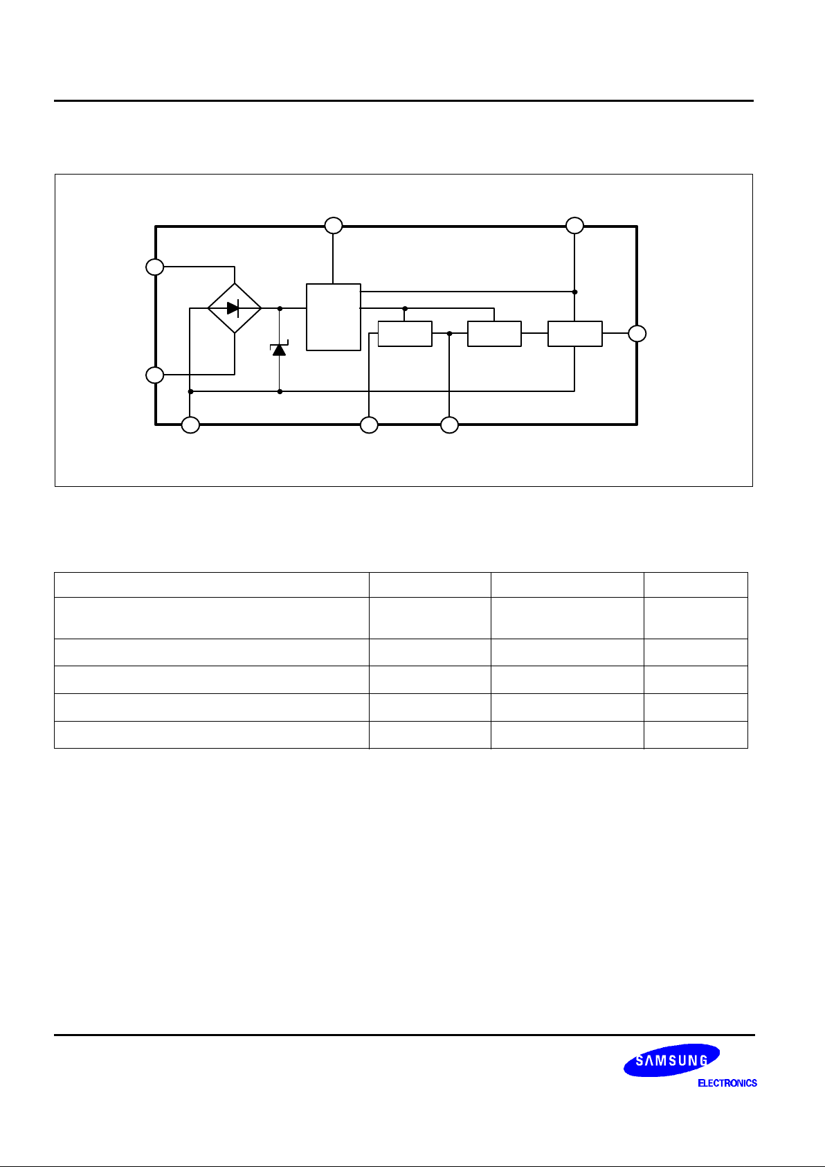
BLOCK DIAGRAM
ABSOLUTE MAXIMUM RATINGS
NOTE: Absolute maximum ratings are those values beyond which permanent damage to the device may occur. These are
stress ratings only and functional operation of the device at or beyond them is not implied. Long exposure to these
conditions may affect device reliability.
Characteristic Symbol Value Unit
Calling Voltage (f = 50Hz) Continuous
Calling Voltage (f = 50Hz)
V
C
120 Vrms
5 sec ON / 10 sec OFF V
C(0N-OFF)
200 Vrms
Supply Current I
CC
22 mA
Operating Temperature T
ORR
−20 — + 70 °C
Storage and Junction Temperature T
STG
−65 — + 150 °C
8
1
7
- +
2
POWER
SUPPLY
CONTROL
CIRCUIT
6
3
5
LOW
FREQ OSC
HIGH
FREQ OSC
OUTPUT
AMP
4
TIP
RING
GND SWEEP RATE
CONTROL
CAPACITOR
OUTPUT FREQUENCY
CONTROL RESISTOR
OUTPUT
ACTIVATION
VOLTAGE ADJUSTABLE
RECTIFIER
CAPACITOR
Page 3

TONE RINGER WITH DRIDGE DIODE S1T2418G01/D02
3
DC ELECTRICAL CHARACTERISTICS (Ta = 25°C)
AC ELECTRICAL CHARACTERISTICS (Ta = 25°C)
Characteristic Symbol Test Conditions Min. Typ. Max. Unit
Operating Voltage V
CC
− − − 26 V
Current Consumption without Load I
CC
VS = 8.8 to 26V − 1.5 1.8 mA
Activation Voltage V
ON
− 12.2 − 13 V
Activation Voltage Range V
ONR
RA = 1KΩ 8 − 10 V
Sustaining Voltage V
SUS
− 8 − 8.8 V
Differential Resistance in Off Condition R
D(OFF)
− 6.4 − − KW
Output Voltage Swing V
0(P-P)
− − VCC−3 − V
Short Circuit Current I
SC
VS = 26V − 35 − mA
Characteristic Symbol Test Conditions Min. Typ. Max. Unit
Output Frequencies
(S1T2418G01)
f
H1
f
H2
VCC = 26V, R1 = 14KΩ
V3 = 0V
V3 = 6
−
−
2300
1700
−
−
Hz
Hz
Output Frequencies
(S1T2418D02)
f
H1
f
H2
VCC = 26V, R1 = 14KΩ
V3 = 0V
V3 = 6V
−
−
1900
1300
−
−
Hz
Hz
fH1 Range f
H1R
R1 = 27kΩ to 1.7kΩ 0.1 − 15 kHz
Sweep Frequency f
S
R1 = 14kΩ, C1 = 100nF − 10 − kHz
Page 4

S1T2418G01/D02 TONE RINGER WITH BRIDGE DIODE
4
APPLICATION CIRCUIT
Device
S1T2418G01 S1T2418D02
Function
f
H1
fH1 (R1 = 14kΩ) 2300 + 300 (Hz) 1900 + 100 (Hz)
fH2 (R1 = 14kΩ) 1700 + 300 (Hz) 1300 + 100 (Hz)
+
8 6 5
7
1 2 3 4
TIP
RING
1uF, 250Vac
C2
C3
10uF
Vs
KA2418B/28
2.2K
R2
R3
224
10K 10K
Piezo
Vout
C1
100nF
R1
12K
1300Ω : 8Ω
f
H1
3.22104×
R1 K()
----------------------------= f
H2
5
7
---f1⋅= f
S
1000
C1 nF()
---------------------=
S1T2418G01
S1T2418D02
2.66104×
R1 K()
----------------------------
3.2210×
4
R1 K()
----------------------------
 Loading...