

Page 1

查询S1M8831A供应商
FRACTIONAL-N RF/INTEGER-N IF DUAL PLL S1M8831A/33
INTRODUCTION
24-QFN-3.5×4.5
The S1M8831A/33 is a Fractional-N frequency synthesizer with integrated
prescalers, designed for RF operation up to 1.2GHz/K-PCS and for IF
operation up to 520MHz. The fractional-N synthesizer allows fast-locking,
low phase noise phase-locked loops to be built easily, thus having rapid
channel switching and reducing standby time for extended battery life. The
S1M8831A/33 based on ∑ - ∆ fractional-N techniques solves the fractional
spur problems in other fractional-N synthesizers based on charge pump
compensation. The synthesizer also has an additional feature that the
PCS/CDMA channel frequency in steps of 10kHz can be accurately
programmed.
The S1M8831A/33 contains dual-modulus prescalers. The S1M8831A RF
synthesizer adopts an 8/9 prescaler (16/17 for the S1M8833) and the IF
synthesizer adopts an 8/9 prescaler. Phase detector gain is user-programmable for maximum flexibility to
address IS-95 CDMA and IMT2000. Various program-controlled power down options as well as low supply
voltage help the design of wireless cell phones having minimum power consumption.
Using the Samsung's proprietary digital phase-locked-loop technique, the S1M8831A/33 has a linear phase
detector characteristic and can be used for very stable, low noise PLLs. Supply voltage can range from 2.7V to
4.0V. The S1M8831A/33 is available in a 24-QFN package.
FEATURES
• High operating frequency dual synthesizer
— S1M8831A: 0.71 to 1.2GHz(RF)/ 45 to 520MHz(IF)
— S1M8833: 1.6 to 1.65GHz(RF)/ 45 to 520MHz(IF)
• Operating voltage range: 2.7 to 4.0V
• Low current consumption (S1M8831A: 5.0mA, S1M8833: 7.0mA)
• Selectable power saving mode (ICC = 1uA typical @ 3V)
• Dual-modulus prescaler and Fractional-N/Integer-N:
— S1M8831A (RF) 8/9 Fractional-N
— S1M8833 (RF) 16/17 Fractional-N
— S1M8831A/33 (IF) 8/9 Integer-N
• Excellent in-band phase noise ( – 85dBc/Hz @ PCS, -90dBc/Hz @CDMA)
Improved fractional spurious performance ( < 80dBc)
• Frequency resolution (= 10kHz/64 @ fref = 9.84MHz)
• Fast channel switching time: < 500us
• Programmable charge pump output current: from 50uA to 800uA in 50uA steps
• Programmability via on-chip serial bus interface
1
Page 2
S1M8831A/33 FRACTIONAL-N RF/INTEGER-N IF DUAL PLL
APPLICATIONS
• High-rate data-service cellular telephones (for CDMA): S1M8831A, S1M8833
• High-rate data-service portable wireless communications (for Korean-PCS): S1M8833
• Other wireless communications systems
ORDERING INFORMATION
Device Package Operating Temperature
+S1M8831A01-G0T0
+S1M8833X01-G0T0
+ : New Product
24-QFN-3.5×4.5
-40 to +85C
2
Page 3
FRACTIONAL-N RF/INTEGER-N IF DUAL PLL S1M8831A/33
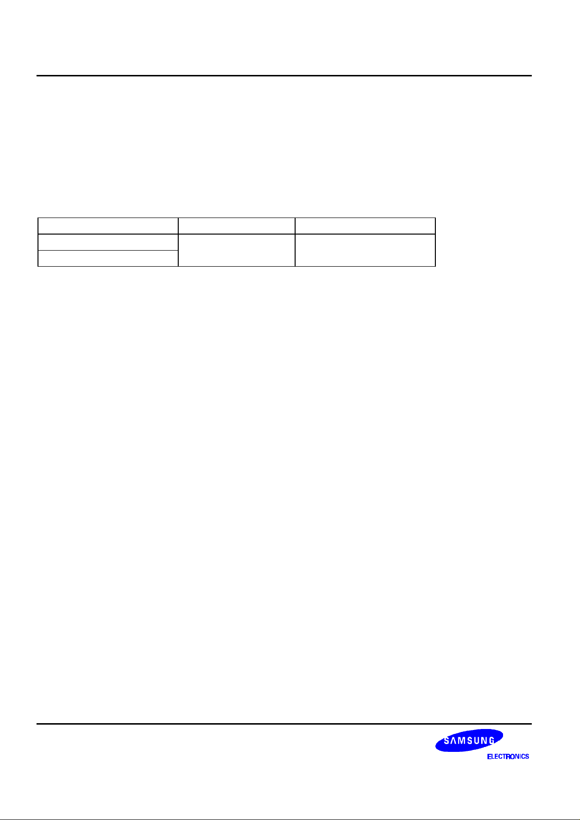
BLOCK DIAGRAM
OUT0 OUT1 VDDIF
24 23 22
VDDRF
VPRF
CPORF
DGND
finRF
finRF
GND
OSCx
1
RF
LD
2
RF
Charge
3
Pump
RF
Phase
Detector
RF Prescaler
4
5
6
+ -
Prescaler
Control
RF
Programmable
Counter
RF N-Latch
foLD Data Out
Multiplexer
IF Prescaler
IF
Programmable
Counter
IF N-Latch
IF
LD
IF
Phase
Detector
Prescaler
Control
IF
Charge
Pump
- +
21
20
19
18
17
VPIF
CPOIF
DGND
finIF
finIF
2-Bit
7
RF
8
Frac-N Latch &
Σ−∆
Modulator
RF R-Latch
24-Bit Shift Register
IF R-Latch
Control
16
15
GND
LE
IF
OSCin
9
RF Reference
Counter
IF Reference
Counter
14
13
DATA
CLOCK
10 11 12
foLD RF_EN IF_EN
3
Page 4
S1M8831A/33 FRACTIONAL-N RF/INTEGER-N IF DUAL PLL
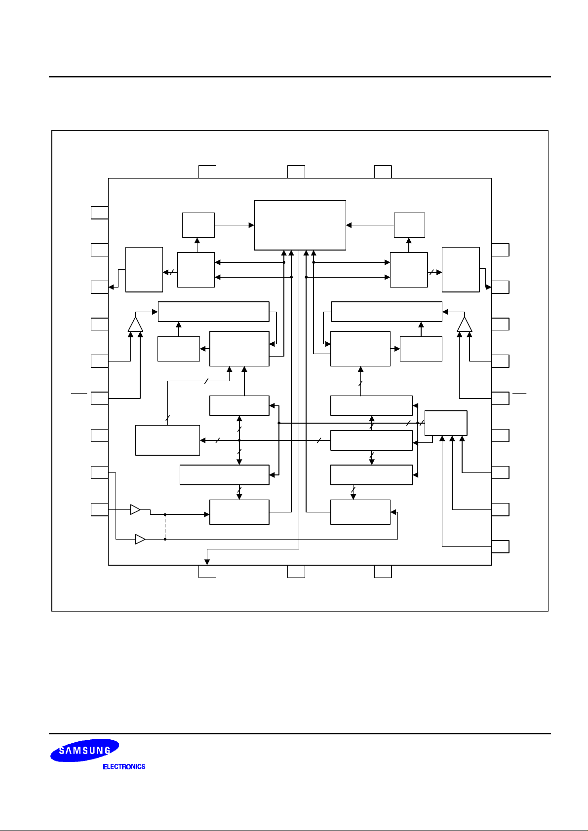
PIN CONFIGURATION
OUT0 OUT1 VDDIF
24 23 22
VPRF
CPORF
DGND
finRF
finRF
GND
RF
OSCx
OSCin
1VDDRF
2
3
4
5
S1M8831A/33
6
7
8
9
21
20
19
18
17
16
15
14
13
VPIF
CPOIF
DGND
finIF
finIF
GND
IF
LE
DATA
CLCOK
10 11 12
foLD RF_EN IF_EN
24-QFN
4
Page 5
FRACTIONAL-N RF/INTEGER-N IF DUAL PLL S1M8831A/33
PIN DESCRIPTION
Pin No. Symbol I/O Description
1
VDDRF
–
RF PLL power supply(2.7V to 4.0V). Must be equal to VDDIF.
2
3
VPRF
CPoRF
–
Power supply for RF charge pump. Must be ≥ VDDRF and VDDIF.
O RF charge pump output. Connected to an external loop filter.
4 DGND – Ground for RF PLL digital circuitry.
5
6
finRF
finRF
I RF prescaler input. Small signal input from the external VCO.
I RF prescaler complementary input. For a single-ended output RF VCO, a
bypass capacitor should be placed as close as possible to this pin and be
connected directly to the ground plane.
7
GND
RF
– Ground for RF PLL analog circuitry.
8 OSCx I RF R counter input (IF_N[22]=0) or not-use (IF_N[22]=1) which can be
configured depending on the state of the program bit IF_N[22].
9 OSCin I Oscillator input to drive both the IF and RF R counter inputs (IF_N[22]=1) or
only the IF R counter (IF_N[22]=0) which can be configured depending on
the state of the program bit IF_N[22].
10 foLD O Multiplexed output of N or R divider and RF/IF lock detect.
11 RF_EN I RF PLL Enable (enable when high, power down when low).
Controls the RF PLL to power down directly, not depending on a program
control. Also sets the charge pump output to be in TRI-STATE when LOW.
Powers up when HIGH depends on the state of RF_CTL_WORD.
12 IF_EN I IF PLL Enable(enable when high, power-down when low).
Controls the IF PLL to power down directly. The same as RF_EN except
that power-up depends on the state of IF_CTL_WORD.
13 CLOCK I CMOS clock input. Data for the various counters is clocked into the 24-bit
shift register on the rising edge.
14 DATA I Binary serial data input. Data entered MSB (Most Significant Bit) first.
15 LE I Load enable when LE goes HIGH. High impedance CMOS input.
16
17
GND
finIF
IF
– Ground for IF analog circuitry.
I IF Prescaler complementary input. For a single-ended output IF VCO, a
bypass capacitor should be placed as close as possible to this pin.
18
finIF
I IF prescaler input. Small signal input from the VCO.
19 DGND – Ground for IF PLL digital circuitry.
20 CPoIF O IF charge pump output. Connected to an external loop filter.
5
Page 6
S1M8831A/33 FRACTIONAL-N RF/INTEGER-N IF DUAL PLL
PIN DESCRIPTION (Continued)
Pin No. Pin Name I/O Descriptions
21
VPIF
–
Power supply for IF charge pump. Must be ≥ VDDRF and VDDIF.
22
23 OUT1 O Programmable CMOS output. Level of the output is controlled by
24 OUT0 O Programmable CMOS output. Level of the output is controlled by
VDDIF
–
IF PLL power supply (2.7V to 4.0V). Must be equal to VDDRF.
RF_N[19] bit.
RF_N[18] bit. In the speedy lock mode, the OUT0 and OUT1 pins can be
utilized as synchronous switches between active low and tri-state.
6
Page 7
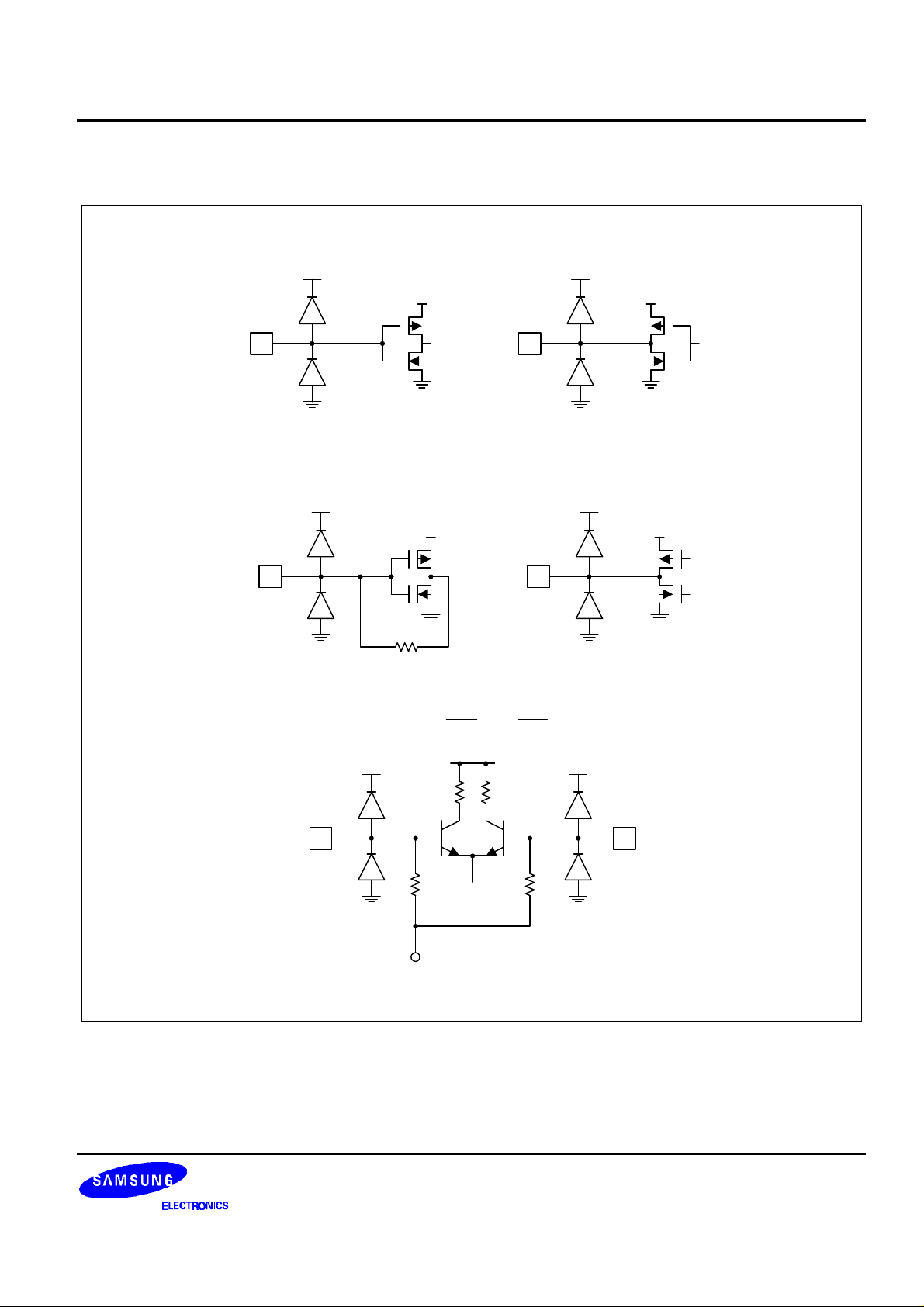
FRACTIONAL-N RF/INTEGER-N IF DUAL PLL S1M8831A/33
EQUIVALENT CIRCUIT DIAGRAM
CLOCK, DATA, LE foLD
OSCin, OSCx CPORF, CPOIF
finRF, finIF
finRF, finRF, finIF, finIF
V
bias
finRF, finIF
7
Page 8
S1M8831A/33 FRACTIONAL-N RF/INTEGER-N IF DUAL PLL
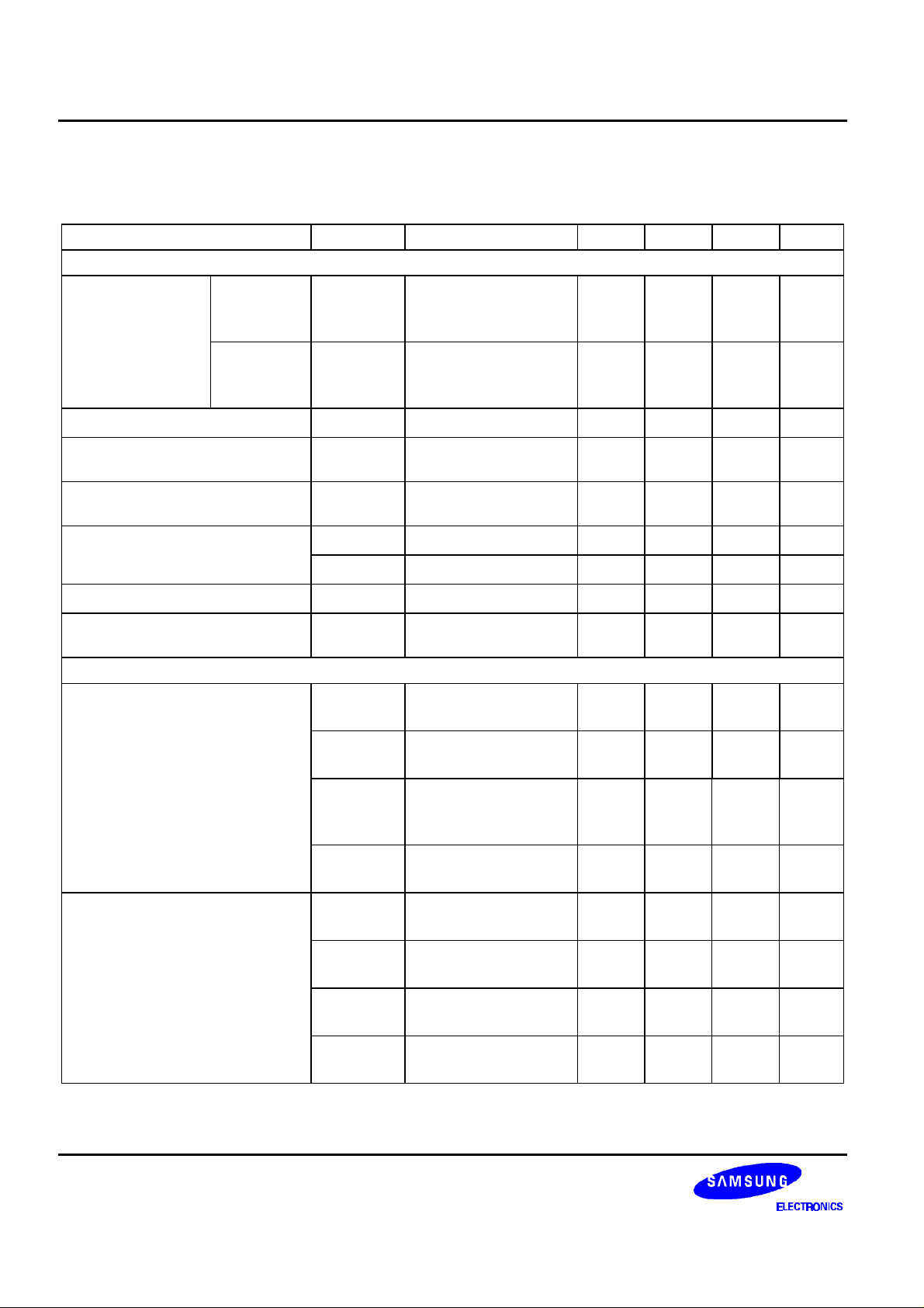
ELECTRICAL SPECIFICATIONS
ABSOLUTE MAXIMUM RATINGS
Characteristics Symbol Value Unit
Power supply voltage
Voltage on any pin with GND = 0 volts
Power dissipation
Operating temperature
Storage temperature
ELECTROSTATIC CHARACTERISTICS
Characteristics Pin No. ESD Level Unit
Human body model All
Machine model All
Charge device model All
V
T
DD
V
P
D
T
STG
0.0 to 4.0 V
I
-0.3 to VDD + 0.3
V
600 mW
a
-40 to +85
-65 to +150
< ± 2000
< ± 300
< ± 800
°C
°C
V
V
V
NOTE: These devices are ESD sensitive. These devices must be handled in an ESD protected environment.
8
Page 9
FRACTIONAL-N RF/INTEGER-N IF DUAL PLL S1M8831A/33
ELECTRICAL CHARACTERISTICS
(V
= 3.0V, VP = 3.0V, Ta = 25°C, unless otherwise specified.)
DD
Characteristic Symbol Test Conditions Min. Typ. Max. Unit
Power supply voltage
Power supply current S1M8831A
RF+IF
S1M8833
V
DD
V
P
I
DD
Fractional-N mode
(f
= 19.68MHz,
osc
2.7 3.0 4.0 V
V
DD
3.0 4.0
5.0 mA
RF R = 2) 7.0
RF+IF
S1M8831A
Quiescent State 3.5
RF+IF
S1M8833
5.5
RF+IF
IF only 1.5
Power down current
I
PWDN
V
DD
= 3.0V
1 10
µA
Digital Inputs: CLOCK, DATA and LE
High level input voltage
Low level input voltage
High level input current
Low level input current
V
IH
V
IL
I
IH
I
IL
V
= 2.7V to 4.0V
DD
V
= 2.7V to 4.0V
DD
V
= V
IH
DD
V
= 0V, V
IL
= 4.0V
= 4.0V
DD
0.7V
DD
0.3V
-1.0 +1.0
-1.0 +1.0
DD
V
V
µA
µA
Reference Oscillator Input: OSCin
Input current
I
IHR
I
ILR
V
IH
V
IL
= V
DD
= 0V, V
= 4.0V
= 4.0V
DD
-100
+100
µA
µA
Digital Output: foLD
High level output voltage
Low level output voltage
V
OH
V
OL
I
= -500µA
out
I
= +500µA
out
VDD-0.4
V
0.4 V
9
Page 10
S1M8831A/33 FRACTIONAL-N RF/INTEGER-N IF DUAL PLL
ELECTRICAL CHARACTERISTICS (Continued)
(V
= 3.0V, VP = 3.0V, Ta = 25°C, unless otherwise specified.)
DD
Characteristic Symbol Test Conditions Min. Typ. Max. Unit
Operating Frequency, Input Sensitivity (Programmable Divider, PFD)
RF operating
frequency
S1M8833
finRF
Fractional-N mode
(f
= 19.68MHz,
osc
1.6 1.65 GHz
RF R = 2)
S1M8831A Fractional-N mode
(f
= 19.68MHz,
osc
0.71 1.2 GHz
RF R = 2)
IF operating frequency
Reference oscillator input
finIF V
OSC
in
DD
= 3.0
45 520 MHz
2 40 MHz
frequency
Phase detector operating
f
PD
10 MHz
frequency
P
RF input sensitivity
IF input sensitivity
Reference oscillator input
RF VDD = 3.0V
fin
V
DD
P
IF V
V
OSCin
fin
DD
= 4.0V
= 2.7V to 4.0V
-15 0 dBm
-10 0 dBm
-10 0 dBm
0.5
V
DD
V
PP
sensitivity
Charge Pump Outputs: CPoRF, CPoIF
RF charge pump output current
IF charge pump output current
I
CPRF-
SOURCE_min
I
CPRF-
SIINK_min
I
CPRF-
SOURCE_
max
I
CPRF-
SIINK_max
I
CPRF-
SOURCE_min
I
CPRF-
SIINK_min
I
CPRF-
SOURCE_max
I
CPRF-
SIINK_max
VCP = VP/2,
RF_CP_WORD=0000
V
= VP/2,
CP
RF_CP_WORD=0000
V
= VP/2,
CP
RF_CP_WORD=1111
V
= VP/2,
CP
RF_CP_WORD=1111
V
= VP/2,
CP
CP_GAIN_8=0
V
= VP/2,
CP
CP_GAIN_8=0
V
= VP/2,
CP
CP_GAIN_8=1
V
= VP/2,
CP
CP_GAIN_8=1
-50 uA
+50 uA
-800 uA
+800 uA
-100 uA
+100 uA
-800 uA
+800 uA
10
Page 11

FRACTIONAL-N RF/INTEGER-N IF DUAL PLL S1M8831A/33
ELECTRICAL CHARACTERISTICS (Continued)
(V
= 3.0V, VP = 3.0V, Ta = 25°C, unless otherwise specified.)
DD
Characteristic Symbol Test Conditions Min. Typ. Max. Unit
Charge pump leakage current
I
CPL
0.5V ≤ VCP ≤ VP-
-2.5 +2.5 nA
0.5V
Sink vs. Source mismatch
Output current magnitude
variation vs. Voltage
I
CP-SIINK
I
CP-SOURCE
ICP vs V
vs
CP
VCP = VP/2
0.5V ≤ V
CP
≤ VP-0.5V
3 10 %
10 15 %
Output current vs.
Temperature
Serial Data Control
CLOCK frequency
CLOCK pulse width high
CLOCK pulse width low
DATA set up time to CLOCK
rising edge
DATA hold time after CLOCK
rising edge
LE pulse width
CLOCK rising edge to LE
rising edge
ICP vs T
f
CLOCK
t
CWH
t
CWL
t
DS
t
DH
t
LEW
t
CLE
V
A
CP
= VP/2
10 %
10 MHz
50 ns
50 ns
50 ns
10 ns
50 ns
50 ns
11
Page 12

S1M8831A/33 FRACTIONAL-N RF/INTEGER-N IF DUAL PLL
FUNCTIONAL DESCRIPTION
finRF
finRF
CLOCK
DATA
LE
OSCx
OSCin
finIF
finIF
+
-
+
-
RF
Prescaler
Serial Data Control
R Counter
R Counter
IF
Prescaler
RF
N Counter
∑ - ∆
Modulator
RF
IF
IF
N Counter
RF
Phase
Detector
RF
LD
foLD
Data Out
Multiplexer
IF
LD
IF
Phase
Detector
RF
Charge
Pump
CMOS
Output
MUX
CMOS
Output
MUX
IF
Charge
Pump
CPoRF
OUT0
foLD
OUT1
CPoIF
The Samsung S1M8831A/33 is RF/IF dual frequency synthesizer IC which supports Fractional-N mode for RF
PLL and Integer-N mode for IF PLL depending on a program control. S1M8831A/33 combined with external
LPFs and external VCOs forms PLL frequency synthesizer. The frequency synthesizer consists of prescalers,
pulse-swallowed programmable N counters, programmable reference R counters, phase detectors,
programmable charge pumps, analog LD (Lock Detector), serial data control, etc.
An input buffer in the prescalers amplifies an RF input power of -10dBm from external RF/IF VCOs to a
sufficient ECL switching level to drive the following ECL divider so that it can normally operate even in a smaller
input power less than -10dBm. The amplified VCO output signal is divided by the prescaler with a pre-determined
divide ratio (div. 8/9 in S1M8831A, div. 16/17 in S1M8833, div. 8/9 in IF), the N counter, or the Fractional-N
circuitry ( Σ - ∆ modulator). External reference signal is divided by the R counter to set the comparison frequency
of the PFD. The divide ratios of the programmable counters can be programmed via the serial bus interface.
These two signals drive the both inputs of the phase detector. The phase detector drives the charge pump by
comparing frequencies and phases of the above two signals. The charge pump and the external LPF make the
control voltage for the external VCO and finally the VCO generates the appropriate frequency signal.
12
Page 13

FRACTIONAL-N RF/INTEGER-N IF DUAL PLL S1M8831A/33
When the PLL is in the locked state, the RF VCO's frequency will be N
frequency, where N
is the integer divide ratio and N
INT
is the fractional component.
FRAC
INT
+ N
times the comparison
FRAC
The S1M8831A/33 has new improved features compared to conventional Integer-N PLLs.
The Fractional-N PLL is available for the RF. The fractional synthesis allows the PFD comparison frequency to
be increased while maintaining the same channel frequency as in AMPS and IS-95A/B/C. It makes possible to
widen a loop bandwidth as wide as 20kHz or more for a faster lock-up time and to improve in-band phase noise
performance due to a reduced divide ratio N. Such S1M8831A/33 in the Fractional-N mode is suitable for CDMA,
GSM and Korean PCS band applications.
Also, from the programmability of the charge pump, the user can easily design a stable loop due to free selection
of loop components and reach to a low spurs, a low power PLLs due to an optimized current selection.
Prescaler
The RF/IF prescaler consists of a differential input buffer and ECL frequency dividers. The input buffer amplifies
an input signal from an external VCO to the required level set by sensitivity requirements. The output of the
amplifier delivers a differential signal to the divider with the correct DC level. The buffer may be either singleended or differentially driven. The single-ended operation is preferred in typical applications due to external VCO.
In this case, we recommend that the complementary input fin of the input buffer be AC coupled to ground through
external capacitors, even though it is internally coupled to ground via an internal 10pF capacitor. The other input
pin fin of the buffer also needs external capacitor for decoupling the DC component and controlling the input
power level.
The RF prescalers of S1M8831A and S1M8833 provide 8/9 and 16/17 prescaler ratio, respectively. The IF
prescaler of S1M8831A/33 contains 8/9 dual modulus prescaler.
Reference Oscillator Inputs
The reference oscillator frequency is provided by an external reference such as TCXO the OSCin and OSCx
pins. When the OSC bit is LOW, the oscillator input pins (OSCin and OSCx) drive the IF R and R counters
separately. When the OSC bit is HIGH, on the other hand, the oscillator input pin OSCin drives both IF R and RF
R counters.
Programmable Dividers (RF/IF N Counters)
The RF N counter can be configured as a fractional counter. The fractional-N counter is selected when the FracN_SEL bit becomes HIGH.
In the fractional mode, the S1M8831A is capable of offering a continuous integer divide range from 72 to 1008
and the S1M8833 offering a continuous integer divide range from 161 to 168.
The S1M8831A/33 IF N counter supports an integer counter mode only, not including fractional counter, and is
capable of operating from 45MHz to 520MHz offering a continuous integer divide range from 72 to 32767.
13
Page 14

S1M8831A/33 FRACTIONAL-N RF/INTEGER-N IF DUAL PLL
∑∑ - ∆∆ Modulator
The RF part of S1M8831A/33 adopts the Σ -∆ modulator as a core of the fractional counter that makes it possible
to obtain divide ratio N to be a fractional number between two contiguous integers. The Σ -∆ modulator effectively
randomizes the quantization noise generated from digitizing process and results in extreme suppression of inband noise power by pushing it out to out-of-band as in conventional Σ -∆ data converter. This technique
eliminates the need for compensation current injection into the loop filter and improves fractional spurious
performance, suitable for high-tier applications.
The ∑-∆ modulator operates only for fractional-N mode, when the Frac-N_SEL is HIGH.
For proper use of the fractional mode, the user should be kept in mind that
1. A fractional number should be set in the range from -0.5 to 0.5 in step of 1/62976.
2. The clock frequency fixed at 9.84MHz ( = 19.68MHz/2) is recommended for the ∑-∆ modulator which is an
optimum condition for achieving better electrical performances related to the fractional noise and power
consumption. Only when using the clock frequency, the S1M8831A/33 guarantees the exact frequency
resolutions: 10kHz for CDMA PCS and 30kHz for CDMA cellular.
Note that the clock frequency much lower than 9.84MHz can deteriorate the fractional noise performance.
Phase-Frequency Detector (PFD) and Charge Pump (CP)
The RF/IF phase detector composed of PFD and CP outputs pump current into an external loop filter in
proportional to the phase difference between outputs of N and R counter . The phase detector has a better linear
transfer characteristic due to a feedback loop to eliminate dead zone. The polarity of the PFD can be
programmed using RF_PFD_POL/IF_PFD_POL depending on whether RF/IF VCO characteristics are positive or
negative. (programming descriptions for phase detector polarity)
Power-Down (or Power-Save) Control
Each PLL is individually power controlled by the enable pins (RF_EN and IF_EN pins) or program control bits
(PWDN, PWDN_RF/IF). The enable pins override the program control bits. When both enable pins are HIGH, the
program control bits determine the state of power control. Power down forces all the internal blocks to be
deactivated and the charge pump output to be in the TRISTATE. The control register, however, remains active
for serial programming and is capable of loading and latching in data during the power down.
14
Page 15

FRACTIONAL-N RF/INTEGER-N IF DUAL PLL S1M8831A/33
PROGRAMMING DESCRIPTION
The S1M8831A/33 can be programmed via the serial bus interface. The interface is made of 3 functional signals:
clock, data, and latch enable(LE). Serial data is moved into the 24-bit shift register on the rising edge of the
clock. These data enters MSB first. When LE goes HIGH, data in the shift register is moved into one of the 4
latches (by the 2-bit control).
LSBMSB Data Flow (MSB First)
DATA[23:2] CTL[1:0]
Control Bit Map (CTL[1:0])
Control Bits Data Location
CTL2(CTL[1]) CTL1(CTL[0]
0 0 RF/IF R counter
0 1 IF N counter
1 0 RF N counter
1 1 RF Frac counter
Data Bit Map (DATA[23:2])
First Bit Register Bit Location Last Bit
23 22 21 20 19 18 17 16 15 14 13 12 11 10 9 8 7 6 5 4 3 2 1 0
RIF_R TEST IF_R_CNTR(15 bits) 0 0
IF_N TEST OSC IF_CTL_
WORD
RF_N RF_CTL_WORD CMOS RF_CP_WORD RF_NB_CNTR(7 bits) FoLD(4 bits) 1 0
RF_Frac RF_NA_CNTR(4 bits) TEST FRAC_CNTR(17 bits) 1 1
NOTE: Test bits are reserved and should be set to be zero(Low) for normal usage.
IF_CP_
WORD
IF_NB_CNTR(3 bits) IF_NA_CNT
R(3 bits)
0 1
15
Page 16

S1M8831A/33 FRACTIONAL-N RF/INTEGER-N IF DUAL PLL
Control Words Control bits Acronym LOW (0) HIGH (1) Comments
OSC IF_N[22] OSC Separate inputs;
OSCin: for IF,
OSCx: for RF
Common input
through OSCin for
both RF and IF
Reference
oscillator input
control
IF_CTL_WORD IF_N[21] IF_CNT_RST Normal operation IF counter reset IF
IF_N[20] PWDN_IF Power up Power down IF
IF_N[19] PWDN Asynchronous
power down
Synchronous
power down
RF and IF
IF_CP_WORD IF_N[18] IF_CP_GAIN 1X 8X IF charge pump
IF_N[17] IF_PFD_POL Negative slope Positive slope IF PFD
RF_CTL_WORD RF_N[23] RF_CNT_RST Normal operation RF counter reset RF
RF_N[22] PWDN_RF Power up Power down RF
RF_N[21] Frac-N_SEL Integer-N mode Fractional-N
mode
RF; PLL mode
selection
CMOS RF_N[20] Speedy_Lock CMOS output Speedy Lock
mode
RF_N[19] OUT1 Voltage LOW Voltage HIGH pin #23
RF_N[18] OUT0 Voltage LOW Voltage HIGH pin #24
RF_CP_WORD RF_N[17:14] RF_CP_LVL Select 16-level charge pump current
RF charge pump
(RF charge pump gain for control
codes in detail)
RF_N[13] RF_PFD_POL Negative slope Positive slope RF PFD
foLD RF_N[5:2] foLD Select LDs and monitoring mode of
internal counters. (foLD control for
Lock Detector
(LD), test mode
control codes in detail)
— Counter reset mode resets R & N counters.
— IF charge pump current can be selected to high current (8X) or low current (1X) mode.
— In the Speedy Lock mode, the OUT0 and OUT1 pins can be utilized as synchronous switches between active
low and tri-state. The Speedy Lock mode activates the OUT0 and OUT1 pins to be connected to GROUND
with a low impedance (< 150Ω) while a high charge pump gain (≥ S 8X) is selected and otherwise to the
TRISTATE.
— For using a programmable CMOS output, the CMOS output bit(RF_N[20]=L) should be activated and then
the desired logic level should be programmed with the control bits RF_N[18] for OUT0 and RF_N[19] for
OUT1.
16
Page 17

FRACTIONAL-N RF/INTEGER-N IF DUAL PLL S1M8831A/33
Programmable Reference Counter (IF_R_CNTR[16:2])
If the control bit is 00, data is moved from the 24-bit shift register into the R-latch which sets the IF reference
counter. Serial data format is shown in the table below.
LSBMSB RIF_R[23:0]
TEST
23 17 16 2 1
Reserved for Test
IF_R_CNTR[16:2] ; 3 ~ 32767 0
Division Ratio of the IF R Counter,
IF_R_CNTR(RI)
Control Bits
0
• 15-Bit IF R Counter Division Ratio
Division ratio: 3 to 32767 (The divide ratios less than 3 are prohibited)
Data are shifted in MSB first
Division Ratio RI RI RI RI RI RI RI RI RI RI RI RI RI RI RI
14 13 12 11 10 9 8 7 6 5 4 3 2 1 0
3 0 0 0 0 0 0 0 0 0 0 0 0 0 0 0
4 0 0 0 0 0 0 0 0 0 0 0 0 0 0 0
• • • • • • • • • • • • • • • •
32767 1 1 1 1 1 1 1 1 1 1 1 1 1 1 1
0
• RF R Counter Division Ratio
Division Ratio: 2 (fixed value. Note it is not programmable.)
17
Page 18

S1M8831A/33 FRACTIONAL-N RF/INTEGER-N IF DUAL PLL
Programmable Counter (N CoUnter)
If the control bits are 01(IF), 10, and 11(RF), data is transferred from the 24-bit shift register into the N/Frac-latch.
N Counter consists of swallow counter (A counter; 3-bit for IF & S1M8831A RF and 4-bit for S1M8833), main
counter (B counter; 7-bit for S1M8831A/33 RF and 12-bit for IF), and fractional counter (F counter; 17-bit for
S1M8831A/33 RF). Serial data format is shown below.
IF N Counter
LSBMSB IF_N[23:0]
IF_CTL_
TEST OSC
23 19 18 2 1
22
WORD
[21:19]
21 17 16 5 4
Program Code Division Ratio of the IF N Counter
IF_CP-WORD
[18:17]
IF_NB_CNTR[16:5] ; 3 - 4095 1
IF_NA_CNTR
[4:2] ; 0 - 7
Control Bits
0
0
•• IF Main Counter Division Ratio (B Counter)
IF_NB_ CNTR[16:5] ; for S1M8831A/33
Division Ratio(B) N N N N N N N N N N N N
11 10 9 8 7 6 5 4 3 2 1 0
3 0 0 0 0 0 0 0 0 0 0 1 1
4 0 0 0 0 0 0 0 0 0 1 0 0
• • • • • • • • • • • • •
4095 1 1 1 1 1 1 1 1 1 1 1 1
Division Ratio: 3 to 4095 (The division ratios less than 3 are prohibited)
• Swallow Counter Division Ratio (A Counter)
IF_NA_CNTR[4:2] ; for S1M8831A/33
Division Ratio(A) N N N
2 1 0
0 0 0 0
1 0 0 1
• • • •
7 1 1 1
Division Ratio: 0 to 7 (B > A)
18
Page 19

FRACTIONAL-N RF/INTEGER-N IF DUAL PLL S1M8831A/33
RF N Counter
LSBMSB RF_N[23:0]
RF_CTL_WORD
[23:21]
23 20 2 1
RF_NA_CNTR
[23:20]
CMOS[20:18] FoLD[5:2]
21 18 17 6 5
Program Code
TEST FRAC_CNTR[18:2] 11
RF_CP_WORD
[17:13]
13 12
RF_NB_CNTR[12:16] ; 3 - 127 0
Division Ratio of the
RF N Counter
Control Bits
RF_Frac[23:0]
•• RF Main Counter Division Ratio (B Counter)
RF_NB_ CNTR[12:6] ; for S1M8831A/33
Division Ratio(B) N N N N N N N
6 5 4 3 2 1 0
3 0 0 0 0 0 1 1
4 0 0 0 0 1 0 0
• • • • • • • •
127 1 1 1 1 1 1 1
1
0
Division Ratio: 3 to 127 (The division ratios less than 3 are prohibited)
•• RF Swallow Counter Division Ratio (A Counter)
RF_NA_CNTR[23:20] ; for S1M8831A RF_NA_CNTR[23:20] ; for S1M8833
Division Ratio(A) N N N N Division Ration(A) N N N N
3 2 1 0 3 2 1 0
0 x 0 0 0 0 0 0 0 0
1 x 0 0 1 1 0 0 0 1
• • • • • • • • • •
7 x 1 1 1 15 1 1 1 1
Division Ratio: 0 to 7 (B > A) Division Ratio: 0 to 15 (B > A)
x = Don' t care condition
19
Page 20

S1M8831A/33 FRACTIONAL-N RF/INTEGER-N IF DUAL PLL
RF Fractional Counter
MSB
RF_NA_CNTR
[23:20]
23 19
Program Code
TEST FRAC_CNTR[18:2] 11
20 18
RF_Frac[23:0]
2 1 0
Division Ratio of the RF Fractional Counter
Control Bits
LSB
• RF Fractional Counter Value (F Counter)
FRAC_ CNTR[18:2] ; for S1M8831A/33 RF
Counter F F F F F F F F F F F F F F F F F
Value(F) 16 15 14 13 12 11 10 9 8 7 6 5 4 3 2 1 0
31488 0 0 1 1 1 1 0 1 1 0 0 0 0 0 0 0 0
• • • • • • • • • • • • • • • • • •
2 0 0 0 0 0 0 0 0 0 0 0 0 0 0 0 1 0
1 0 0 0 0 0 0 0 0 0 0 0 0 0 0 0 0 1
0 0 0 0 0 0 0 0 0 0 0 0 0 0 0 0 0 0
-1 1 1 1 1 1 1 1 1 1 1 1 1 1 1 1 1 1
-2 1 1 1 1 1 1 1 1 1 1 1 1 1 1 1 1 0
• • • • • • • • • • • • • • • • • •
-31488 1 1 0 0 0 0 1 0 1 0 0 0 0 0 0 0 0
F Counter Value: -31488(2's complementary) to 31488
NOTE: For a negative integer, the counter value should be inputted as the corresponding 2's complementary binary code.
For instance, the 2's complementary binary code of -2 is
1 1111 1111 1111 1110.
20
Page 21

FRACTIONAL-N RF/INTEGER-N IF DUAL PLL S1M8831A/33
Programmable PFD and Charge Pump
IF Charge Pump Gain (IF_CP_WORD; IF_N[18])
Control Words Control Bits Acronym LOW (0) HIGH (1) Comments
IF_CP_WORD IF_N[18] IF_CP_GAIN 1X (100uA) 8X (800uA) IF charge pump
RF Charge Pump Gain (RF_CP_WORD; RF_N[17:14])
Control Words Control Bits Acronym LOW (0) HIGH (1) Comments
RF_CP_WORD RF_N[17:14] RF_CP_LVL Select 16-level charge
RF charge pump
pump current
Icpo (uA) 8X 4X 2X 1X
RF_N[17] RF_N[16] RF_N[15] RF_N[14]
50 0 0 0 0
100 0 0 0 1
• • • • •
200 0 0 1 1
250 0 1 0 0
• • • • •
400 0 1 1 1
450 1 0 0 0
• • • • •
800 1 1 1 1
21
Page 22

S1M8831A/33 FRACTIONAL-N RF/INTEGER-N IF DUAL PLL
Phase Detector Polarity (RF_CP_WORD/IF_CP_WORD; RF_N[13]/IF_N[17])
Depending on VCO characteristics, IF_N[17] and RF_N[13] bits should be set as follows:
Control Bits LOW (0) HIGH (1) Comments
IF_N[17] Negative Slope Positive Slope IF PFD
RF_N[13] Negative Slope Positive Slope RF PFD
VCO Characteristics
(1)
VCO
Output
Frequency
VCO Input
Voltage
(2)
22
Page 23

FRACTIONAL-N RF/INTEGER-N IF DUAL PLL S1M8831A/33
Program Mode Control
Power Down Mode Operation
Control Words Control bits Acronym LOW (0) HIGH (1) Comments
IF_CTL_WORD IF_N[20] PWDN_IF Power Up Power Down IF
IF_N[19] PWDN Asynchronous
Power Down
Synchronous
Power Down
RF and IF
RF_CTL_WORD RF_N[22] PWDN_RF Power Up Power Down RF
Each PLL is individually power controlled by the enable pins (RF_EN and IF_EN pins) or program control bits
(PWDN, PWDN_RF/IF). The enable pins override the program control bits. When both enable pins are HIGH, the
program control bits determine the state of power control. Power down forces all the internal analog blocks to be
deactivated and the charge pump output to be in a TRISTATE. The oscillator circuitry function becomes disabled
dependent on the state of IF and RF power-down bits, IF_N[20] and RF_N[22]. The RF(or IF) oscillator buffer is
powered down when the power down bit (RF_N[22] or IF_N[20]) becomes HIGH. The control register and R/N
counters, however, remains active for permitting serial programming and is capable of loading and latching in
data during the power down. The PLL returns to the active power-up mode when IF_N[20] and RF_N[22] become
LOW.
There are synchronous and asynchronous power-down modes for S1M8831A/33. The power-down bit IF_N[19] is
used to select between synchronous and asynchronous power down. Synchronous power down mode occurs if
IF_N[19] bit is HIGH and then the power down bit (RF_N[22] or IF_N[20]) becomes HIGH. In the synchronous
power down mode, the power-down function will go into power down mode upon the completion of a charge
pump pulse event because it is synchronized with the charge pump and thus can diminish undesired frequency
jumps. Asynchronous power down mode occurs if IF_N[19] bit is LOW and then the power down bit (RF_N[22] or
IF_N[20]) becomes HIGH. Activation of the asynchronous function will go into power-down mode immediately.
RF Power Down Mode Table
RF_N[22] IF_N[19] Power Down Mode Status
0 0 RF PLL active
0 1 RF PLL active, only charge pump to TRISTATE
1 0 Asynchronous power down
1 1 Synchronous power down
IF Power Down Mode Table
IF_N[20] IF_N[19] Power Down Mode Status
0 0 IF PLL active
0 1 IF PLL active, only charge pump to TRISTATE
1 0 Asynchronous power down
1 1 Synchronous power down
23
Page 24

S1M8831A/33 FRACTIONAL-N RF/INTEGER-N IF DUAL PLL
Reference Oscillator Input Control
Control Words Control bits Acronym LOW (0) HIGH (1) Comments
OSC IF_N[22] OSC separate inputs;
OSCin: for IF,
OSCx: for RF
common input
through OSCin
for both RF and
IF
reference
oscillator input
control
The reference oscillator frequency is provided from an external reference such as TCXO through the OSCin and
OSCx pins. When the OSC bit is LOW, the oscillator input pins( OSCin and OSCx) drive the IF R and RF R
counters separately. When the OSC bit is HIGH, on the other hand, the oscillator input pin OSCin drives the IF R
and RF R counters commonly.
IF_N[22] = LOW
PWDN_IF PWDN_RF IF RF
IF_N[20] RF_N[22]
0 0
0 1
OSC
OSC
in
in
1 0 LOW(powerdown)
OSC
x
LOW(powerdown)
OSC
x
1 1 LOW(powerdown) LOW(powerdown)
IF_N[22] = HIGH
PWDN_IF PWDN_RF IF RF
IF_N[20] RF_N[22]
0 0
0 1
OSC
OSC
in
in
LOW(powerdown)
1 0 LOW(powerdown)
1 1 LOW(powerdown) LOW(powerdown)
OSC
OSC
in
in
24
Page 25

FRACTIONAL-N RF/INTEGER-N IF DUAL PLL S1M8831A/33
Programmable Counter Reset Control
Control Words Control Bits Acronym LOW (0) HIGH (1) Comments
IF_CTL_WORD IF_N[21] IF_CNT_RST Normal
Operation
RF_CTL_WORD RF_N[23] RF_CNT_RST Normal
IF Counter
IF
Reset
RF Counter Reset RF
Operation
Counter Reset Mode Resets R & N Counters.
RF Fractional-N Selection
Control Words Control Bits Acronym LOW (0) HIGH (1) Comments
RF_CTL_WORD RF_N[21] Frac-N_SEL Reserved Fractional-N Mode RF; PLL Mode
Selection
CMOS Output Control
Control Words Control Bits Acronym LOW (0) HIGH (1) Comments
CMOS RF_N[20] Speedy Lock CMOS Output Speedy Lock Mode
RF_N[19] OUT1 Voltage LOW Voltage HIGH Pin #23
RF_N[18] OUT0 Voltage LOW Voltage HIGH Pin #24
In the Speedy Lock mode, the OUT0 and OUT1 pins can be utilized as synchronous switches between active low
and a tri-state. The Speedy Lock mode activates the OUT0 and OUT1 pins to be connected to GROUND with a
low impedance ( < 150Ω) while a high charge pump gain ( ≥ 8X) is selected and otherwise to a tri-state. For using
a programmable CMOS output, the CMOS output bit(RF_N[20] = LOW) should be activated and then the desired
logic level should be programmed with the control bits RF_N[18] for OUT0 and RF_N[19] for OUT1.
25
Page 26

S1M8831A/33 FRACTIONAL-N RF/INTEGER-N IF DUAL PLL
foLD Control
Control Words Control Bits Acronym LOW (0) HIGH (1) Comments
foLD RF_N[5:2] foLD Select LDs and monitoring mode of
internal counters.
Lock Detector(LD),
Test Mode
foLD[3] foLD[2] foLD[1] foLD[0] foLD Output State
0 0 0 0 Disabled (default LOW)
0 0 0 1 RF and IF analog lock detect
0 0 1 0 Reserved test mode
0 0 1 1 Reserved test mode
X 1 0 0 Reserved test mode
X 1 0 1 IF R counter output
X 1 1 0 IF N counter output
X 1 1 1 RF R counter output
1 0 0 0 RF N counter output
1 0 0 1 Reserved test mode
1 0 1 0 Reserved test mode
1 0 1 1 Reserved test mode
— When the PLL is locked and the analog lock detect mode is selected, the foLD output is HIGH, with narrow
pulses LOW.
Lock Detector (LD)
There is analog mode for S1M8831A/33. The foLD bits, RF_N[5:2], are used to select the lock detection mode
and to output the selected lock signal through the foLD pin.
The foLD output becomes HIGH with narrow pulsed LOW while both RF and IF PLLs are locked and thereby the
output should be low-pass filtered for a DC locked voltage HIGH.
26
Page 27

FRACTIONAL-N RF/INTEGER-N IF DUAL PLL S1M8831A/33
Pulse Swallow Function
The RF VCO's frequency f
becomes N
VCO
INT
+ N
times the comparison frequency (f
FRAC
/R) where NINT
OSC
is the integer divide ratio and NFRAC is the fractional component;
f
VCO
= (N
INT
+ N
FRAC
) ×× f
OSC
/R = N ×× f
OSC
/R
where N
RF PLL: N
IF PLL: N
f
VCO
f
OSC
= (P ×× B) + A,
INT
= F/62976, -31488 ≤≤ F ≤≤ 31488, B > P, and R = 2
FRAC
= 0, B > A, and 3 ≤≤ R ≤≤ 32767
FRAC
: External VCO output frequency
: External reference frequency (From external oscillator)
R : Preset divide ratio of programmable R counter (RF: 2, IF: 3 to 32767);
P : Preset modulus of dual modulus prescaler (S1M8831 RF: P=8, S1M8833 RF: P=16, IF: P=8)
B : Preset value of main counter (S1M8831A/33 RF: 3 to 126, IF: 3 to 4095)
A : Preset value of swallow counter division ratio
(S1M8831 RF: 0 ≤ A ≤ 7, S1M8833 RF: 0 ≤ A ≤ 15, IF: 0 ≤ A ≤ 7, A < B)
N
: Fractional component of Pulse-swallowed division ratio N (for IF: N
FRAC
FRAC
= 0)
F : Preset value of fractional register (-31488 ≤ F ≤ 31488);
For a negative integer, F should be inputted as its 2's complementary binary code.
For examples in S1M8831 fractional-N mode (f
= 19.68MHz, R=2, P=8)
OSC
1) for fvco = 955.02MHz ; N = 97.05487805, B=12, A=1, F=3456 (= 0 0000 1101 1000
0000)
2) for fvco = 955.03MHz ; N = 97.05589431, B=12, A=1, F=3520
3) for fvco = 956.25MHz ; N = 97.17987805, B=12, A=1, F=11328
4) for fvco = 979.35MHz ; N = 99.52743902, B=12, A=4, F=-29760
∴∴ F= 0.52743903 X 62976 = 33125 → 33125 > 31488 (A=3+1=4)
= 33215 – 62976 = -29760 (1 1000 1011 1100 0000)
For examples in S1M8833 fractional-N mode (f
= 19.68MHz, R=2, P=16)
OSC
1) for fvco = 1620.87MHz(CH25) ; N = 164.722561, B=10, A=5, F=-17472 (= 1 1011 1011 1100 0000)
2) for fvco = 1620.88MHz ; N = 164.7235772, B=10, A=5, F=-17408
3) for fvco = 1622.12MHz(CH50) ; N = 164.8495935, B=10, A=5, F=-9472
4) for fvco = 1632.12MHz(CH250) ; N = 165.8658537, B=10, A=6, F=-8448
5) for fvco = 1648.37MHz(CH575) ; N = 167.5172764, B=10, A=8, F=-30400
27
Page 28

S1M8831A/33 FRACTIONAL-N RF/INTEGER-N IF DUAL PLL
Serial Data Input Timing
MSB LSB
DATA
DATA[23]
CTL[0]CTL[1]DATA[22] DATA[10] DATA[9]
CLOCK
t
DS
t
CWL
t
CWH
LE
t
DH
t
CLE
Phase Detector and Charge Pump Characteristics
Phase difference detection range: -2π to +2π
When the positive-slope polarity of PFD is selected, IF_N[17] = HIGH or RF_N[13] = HIGH;
fr
t
LEW
LD
CPo
fp
fr > fp fr = fp fr < fp fr < fp fr < fp
28
Page 29

FRACTIONAL-N RF/INTEGER-N IF DUAL PLL S1M8831A/33
SIMPLIFIED SCHEMATIC DIAGRAM FOR RF SENSITIVITY TEST
2.7V to 4.0V
V
DD
V
P
100pF 100pF 2.2µF2.2µF
RF
Signal
Generator
10dB ATTN
50Ω
Microstrip
100pF
51Ω 100pF
OSC
f
in
f
in
S1M8831A
in
/33
LE
foLD
DATA
CLOCK
Frequency
Counter
12kΩ
39kΩ
NOTES:
1. Sensitivity limit is determined when the error of the divided RF output (fOLD) becomes 10Hz.
2. f
= 1.0GHz, N = 1000, P = 8, R = 2 in S1M8831 Integer-N test mode
VCO
f
= 1.6GHz, N = 1600, P = 16, R = 2 in 1M8833 Integer-N test mode
VCO
PC Parallel
Port
29
Page 30

S1M8831A/33 FRACTIONAL-N RF/INTEGER-N IF DUAL PLL
TYPICAL APPLICATION CIRCUIT
V
P
100pF 0.01µF
V
DD
100pF 0.01µF
22
Ω
Reference
Input
1000pF
51
Ω
RF Out
100pF
10pF
VCO
10pF
R
in
R3
C3 C2
R1
C1
9 8
OSCin OSCx
foLD
10
foLD
V
DD
11
RF_EN
12
IF_EN
CLCOK DATA LE GND
13 14 15 16 17 18 19 20 21
From
Controller
<RF VCO Module: ALPS Part No>
. CDMA : UCVA4X103A
. K-PCS : UCVW4X102A
. US-PCS : UCVA3X120A
7 6
GND
RF
finRF
IF Out
5 4
finRF DGND
S1M8831A/33
finIF
IF
1000pF
56pF
3 2
CPORF VPRF1VDDRF
finIF DGND CPOIF VPIF
R
in
56pF
VCO
R13
C12C13
R11
C11
0.1µF
OUT0
OUT1
24
23
0.1µF
VDDIF
22
100pF 0.01µF
V
P
100pF 0.01µF
22
Ω
V
DD
NOTE: The role of Rin: Rin makes a large portion of VCO output power go to the load rather than the PLL.
The value of Rin depends on the VCO power level.
30
Page 31

FRACTIONAL-N RF/INTEGER-N IF DUAL PLL S1M8831A/33
PCB LAYOUT GUIDE
In doing PCB layouts for S1M8831A/33, we recommend that you apply the following design guide to your
handsets, thus improving the phase noise and reference spurious performances of the phones.
1. The S1M8831A/33 has external four power supply pins to supply on-chip bias, each for analog and digital
blocks of RF and IF PLLs. Basically in doing PCB layout, it is important that power supply lines should be
separated from one another and thus coupling noises through the voltage supply lines can be minimized.
If you have some troubles with the direction to separate, you can choose the following recommendations for
your convenience;
• Tying analog power lines, VCCRF and VCCIF, is possible.
• Tying digital power lines, VP1 and VP2, is possible.
• A point connecting the analog and digital power lines should be near to battery line as close as possible.
It minimizes coupling noise effects from a digital switching noise into analog blocks. We also recommend
that a passive RC low pass filter (R(22Ω), C(100nF)) be utilized for suppressing high frequency noise on the
analog power supply line and reducing any digital noise couplings.
2. VCO power lines should be well separated from those of PLL because VCO is generally a very sensitive
device from power line noises and PLL is a digital noise generator.
3. For more improvement of reference spurious performance, it is recommended that the LPF ground be tied to
the PLL ground, not the VCO ground.
31
Page 32

S1M8831A/33 FRACTIONAL-N RF/INTEGER-N IF DUAL PLL
PACKAGE DIMENSIONS
1.00MAX
4.50 + 0.10
A
#1 INDEX AREA
3.50 + 0.10
(0.05)
(0.05)
0.27 + 0.05
0.70 + 0.05
B
C
0.08 C
4X0.50 + 0.10
#24
#1
32
2X
2X4.00
0.10 C
20X0.50
2X1.00
24X0.30 + 0.05
0.10
#1 ID MARK
2X
0.10 C
M
B
C
S
C
 Loading...