

Page 1
Preliminary
4.6W AUDIO POWER AMP S1A0067X01
GENERAL DESCRIPTION
The S1A0067X01 is a two channel power amplifier with 4.6W
typical output on 12.0V Vcc.
It’s typical output is 4.6W on VCC = 12.0V. There is no needs
of a bootstrap-capacitor due to the use of V-PNP for a power
transitory.
So, it is an advantage for making a whole system. It has an
additional stand-by function, the pop noise on switc hing it’s
mute function is much reduced.
The S1A0067X01 has the built-in thermal protection function
with hysterisys in order to protect a blocking oscillation in a
short period due to a repeated protection switching on overheating of IC.
The S1A0067X01 has a built-in output-vcc or output-gnd short protection function.
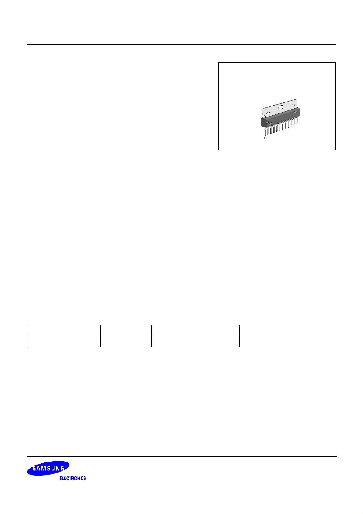
12−SIPH−B
FEATURES
• Two channel 4.6W power Amp (Vcc = 12.0V)
• High power with non bootstrap capacitor
• Mute function
• Stand-by function: 100uA
• Very low pop noise, when mute on/off
• Wide operation voltage: 6.0V − 18.0V
• Include thermal protection with hysterisis
• Output-Vcc, output-GND short protection
ORDERING INFORMATION
Device Package Operation Temperature
S1A0067X01-X0B0 12−SIPH−B −25 − +75°C
1
Page 2
Preliminary
S1A0067X01 4.6W AUDIO POWER AMP
PIN DESCRIPTION
Terminal
Type Description
Name No.
Vcc 3, 12 Vcc, PVCC Power supply
GND 9 GND Ground
INPUT 1,2 6, 7 INPUT Input
NF 1,2 5, 8 NF Pin for negative feedback capacitor
OUTPUT 1, 2 2, 10 OUTPUT Output
RR 4 RR Pin for ripple rejection
STAND-BY 11 ST Pin for stand-by mode
MUTE 1 MT Pin for mute function control
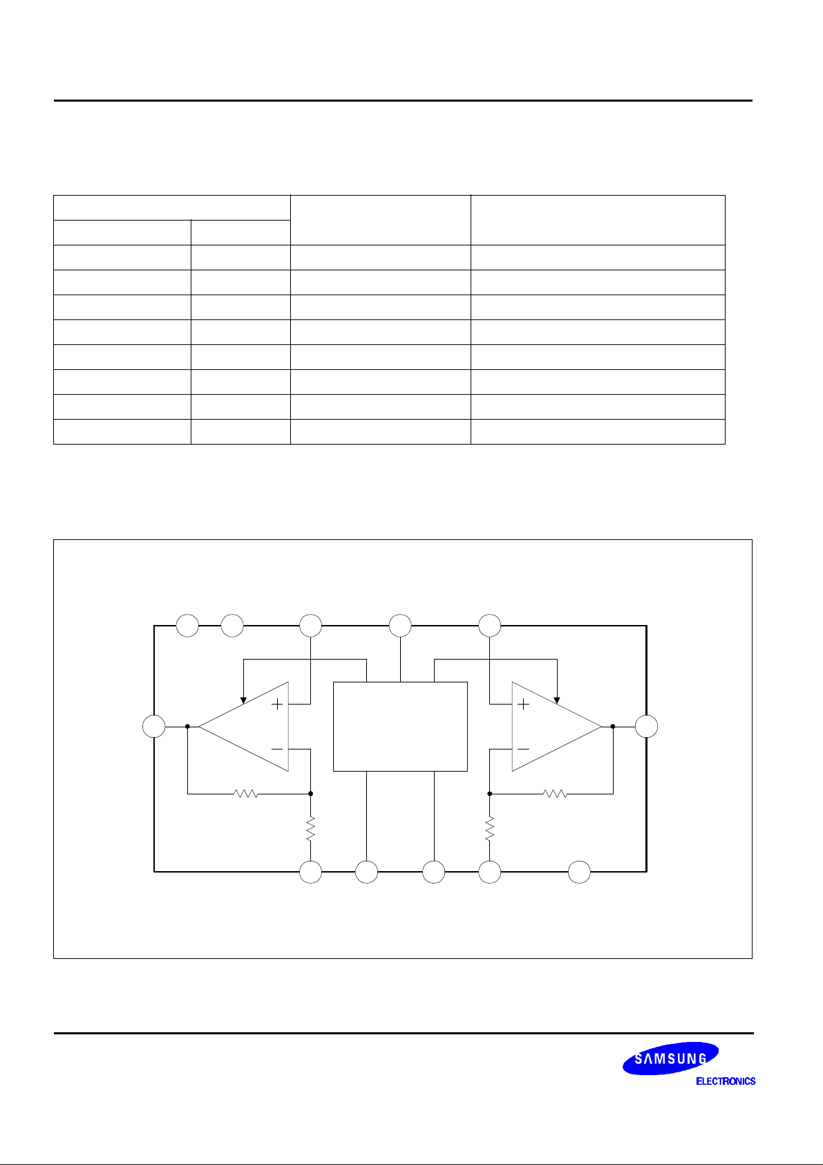
BLOCK DIAGRAM
INPUT2RRINPUT1PVCCVCC
3 12
6
4
7
2
OUTPUT1
CH1 CH22
5
NF1 MUTE STAND-BY NF2 GND
BIAS
&
PROTECTION
1 11 9
8
10
OUTPUT2
Page 3

Preliminary
RIPPLE REJECTION
PVCC
4.6W AUDIO POWER AMP S1A0067X01
PIN CONFIGURATION
S1A0067X01
1 2 3 4 5 6
OUTPUT1
MUTE CONTROL
VCC
NF1
INPUT1
INPUT2
NF2
GND
OUTPUT2
STADN-BY
ABSOLUTE MAXIMUM RATINGS
Parameter System Ratings Unit
Maximum supply voltage VCCmax 18 V
Maximum supply current Ipeak 2.5 A
Power Dissipation Pd 12.5 W
Operating temperature Topr − 12 — 75 °C
121110987
Storage temperature Tstg − 40 — 150 °C
3
Page 4

Preliminary
S1A0067X01 4.6W AUDIO POWER AMP
ELECTRICAL CHARACTERISTICS
(Ta = 25C, Vcc = 9V, RL = 4Ω, f = 1kHz, RG = 600Ω, unless otherwise specified)
Parameter Symbol condition
Min. Typ. Max.
Supply Current Icc Vi = 0 − 20 45 mA
Standby Current Isb Vpin11 = 0 − − 100 uA
Po1 THD = 10% 2.0 2.5 − W
Maximum Power
Po2 THD 10%, Vcc = 12.0V 4.0 4.6 − W
THD THD Po = 1W − 0.1 0.9 %
AV1 Rf = 51Ω, Vo = 0.775V 38 40 42 dB
Voltage Gain
AV2 Rf = 0Ω, Vo = 0.775V 44 46 48 dB
Channel Balance CB Rf = 0Ω, Vo = 0.775V − 2.0 0.0 2.0 dB
Input Resistance Ri − 32 40 48 kΩ
Output Noise Vno Rg = 10Ω, BW = 20 — 20kHz − 0.2 1.0 mVrms
Ripple Rejection Ratio RR Rg = 600Ω, f = 120kHz 46 − − dB
Channel Crossover Ratio CT Rg = 10Ω, f = 1kHz, Vo = 0dBm 40 − − dB
Standby Changing Voltage Vsb − 0 − 0.9 V
Mute Changing Voltage Vmt − 0 − 0.25 V
Mute Attenuation Ratio Rmt Vpin1 = 0 − − -60 dB
Spec
Unit
4
Page 5

Preliminary
4.6W AUDIO POWER AMP S1A0067X01
APPLICATION CIRCUIT
S1A0067X01
SW1
Vmt = 0.25V
1 2 3 4 5 6
0.1µF
1000µF
RL = 4
Ω
VM VM
47µF
47µF
4.7µF
4.7µF
SW3
SW5
47µF
600
10k
120
Ω
Ω
i1
V
121110987
0.1µF
1000µF
Ω
RL = 4
Ω
600
Ω
10k
Ω
SW4
i2
V
AM
1000µF
0.1µF
VCC
SW6
Vst = 0.9V
5
Page 6

Preliminary
S1A0067X01 4.6W AUDIO POWER AMP
APPLICATION CIRCUIT 1
S1A0067X01
1 2 3 4 5 6
0.1µF
47µF 4.7µF 47µF
4.7µF47µF
Vmt
4
SP
1000µF
Ω
SW5
0.1µF
4
SP
Ω
1000µF
121110987
1000µF
0.1µF
VCC
VstVi2Vi1
6
 Loading...