

Page 1
S175 - 50
175 Watts, 50 Volts, Class AB
Milcom 1.5 - 30
GENERAL DESCRIPTION
The S175-50 is a 50 Volt, COMMN EMITTER device designed for Class A,
AB or C operation in the HF/VHF frequency bands. Its high collector voltage
simplifies the design of wideband, SSB linear amplifiers. The transistor chip is
built using Gold Topside Metal, diffused emitter ballast resistors and silicon
nitride passivation, providing the user with the Highest MTTF available.
ABSOLUTE MAXIMUM RATINGS
Maximum Power Dissipation @ 25 C 270 Watts
Maximum Voltage and Current
BVces Collector to Emiter Voltage 110 Volts
BVebo Emitter to Base Voltage 4.0 Volts
Ic Collector Current 20 A
Ma ximum Temperatures
Storage Temperature - 65 to +150 C
Operating Junction Temperature +200 C
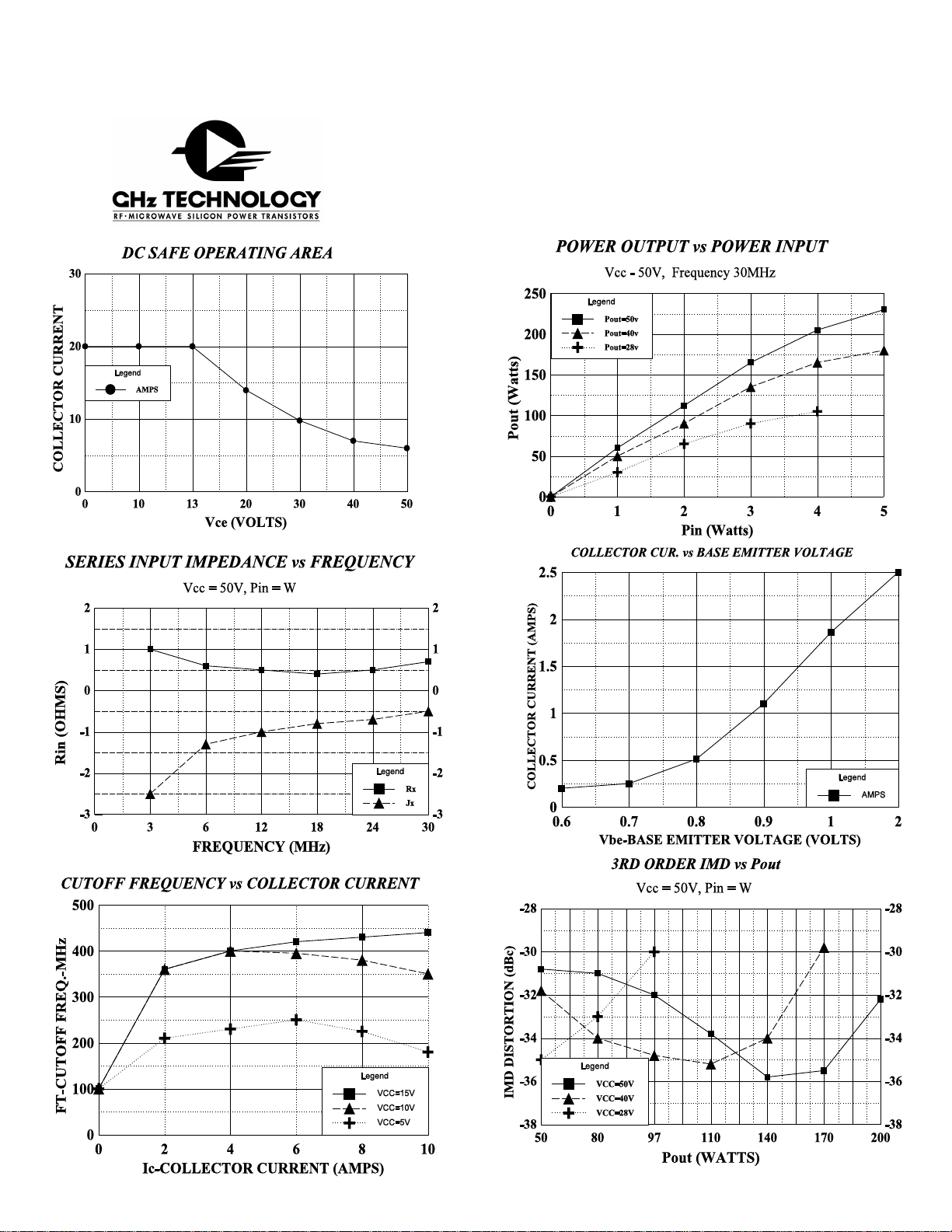
ELECTRICAL CHARACTERISTICS @ 25 C
SYMBOL CHARACTERISTICS TEST CONDITIONS MIN TYP MAX UNITS
o
o
o
O
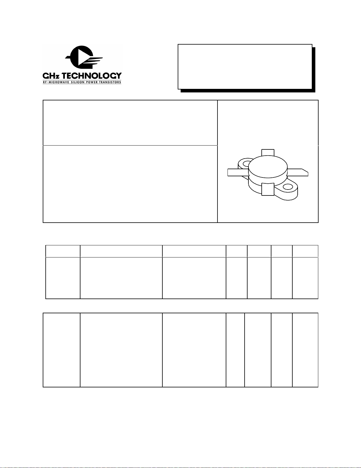
CASE OUTLINE
55HX, Style 2
MHz
Pout
Pin
Pg
η
c
VSWR
BVebo
BVces
BVceo
Zin
ZI
Cob
h
FE
IMD
Initial Issue June, 1994
GHz TECHNOLOGY INC. RESERVES THE RIGHT TO MAKE CHANGES WITHOUT FURTHER NOTICE. GHz RECOMMENDS THAT
BEFORE THE PRODUCT(S) DESCRIBED HEREIN ARE WRITTEN INTO SPECIFICATIONS, OR USED IN CRITICAL APPLICATIONS,
THAT THE PERFORMANCE CHARACTERISTICS BE VERIFIED BY CONTACTING THE FACTORY.
Power Output
Power Input
Power Gain
Efficiency
Load Mismatch Tolerance
Emitter to Base Breakdown
Collector to Emitter
Breakdown
Collector to Emitter
Breakdown
Series Input Impedance
Series Load Impedance
Output Capacitance
DC - Current Gain
Intermodulation Distortion Lev.
F = 30 MHz
Vcc = 50 Volts
At Rated Power Out
Ie = 10 mA
Ic = 100 mA
Ie = 100 mA
At Rated Pout & Freq.
At Rated Pout & Freq.
Vcb = 50 V, Ie = 0
Vce = 5 V, Ic = 2 A
At Rated Pout
175
17
4
110
53
10
17.5
65
0.6-j0.4
4.6+2.1
180
-35
3.5
30:1
Watts
Watts
dB
%
Volts
Volts
Volts
OHMS
OHMS
dBc
GHz Technology Inc. 3000 Oakmead Village Drive, Santa Clara, CA 95051-0808 Tel. 408 / 986-8031 Fax 408 / 986-8120
Page 2
S175-50
Page 3

2-30 MHz, 300 Watts
Linear Amplifier
L2
C5
S175-50
C8
C9
+50V
+
Vbb
-
RF IN
C1
R1
R2
C2
BYI-1
T1
L1
C3
C4
R3
R4
R5
R6
L3 C6
Q1
Q2
C7
T2
T3
C10
RF OUT
Q1,Q2=Ghz S175-50
BYISTOR=GHz BYl-1
C1,C3,C5,C6,C7,C8=0.1mF ceramic
C2=25-240pF Compression Mica
C4=75-480pF Compression Mica
C9=10mF, 50V, Electrolytic
C10=2700pF DM15
L1=6 turns on Indiana General F627-9, H Material
L2,L3=2.2mH, Molded Inductor
R1,R2=22W, 2 Watts
R3,R6=220W, 2 Watts
R4,R5=10W, 1/4 Watt
August 1996
TRANSFORMER DETAILS
T1: 8 beads of Indiana General F625-9, H
material on two brass tubes. The primary is
four turns of #20 vinyl clad wire wound
through the brass tubes
T2: #20 twisted pair, approximately 2 crests
per centimeter, wound on Indiana General
F624-19, H material
T3: 10 beads of Indiana General F627-8,
H materail mounted on two brass tubes. The
secondary consist of 3 #20 vinyl clad wires
in parallel. The three wires should be wound
to produce a 2:1 turns ratio
 Loading...