

Page 1
S11MS3/S21MS3/S21MS4
S11MS3/
S21MS3/S21MS4
■ Features
1. Ultra-compact, mini-flat package type
(3.6 x 4.4 x 2.0mm
2. Built-in zero-cross circuit
(S21MS4
)
3. High isolation voltage between input and
output (V
iso rms
4. Recognized by UL, file No.E64380
■ Model Line-ups
No built-in
zero-cross circuit
Built-in
zero-cross circuit
■ Applications
1. For triggering of medium/high power
triacs
)
: 3 750V
)
For 100V lines For 200V lines
S11MS3 S21MS3
- S21MS4
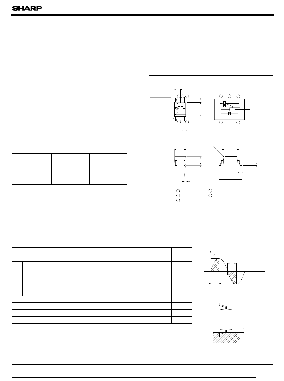
High Density Surface Mount Type
Mini-flat Package
Phototriac Coupler
7.0
5.3
±
+0.2
-
0.3
0.7
(
Unit : mm
456
❈
Zero-cross
circuit
+ 0.4
0.5
-
0.2
± 0.05
0.2
■ Outline Dimensions
±
0.25
1.27
Model No.
S
Anode
mark
13
±
0.3
3.6
6˚
1 Anode
3 Cathode
4 Anode/
cathode
❈ Zero-cross circuit for S21MS4
456
0.4
±
0.1
C0.4
Input side
MAX.
0.6
0.2
±
4.4
0.2
±
2.6
0.1
±
0.1
Internal connection
diagram
13
No external connection
5
6 Anode/
cathode
)
■ Absolute Maximum Ratings
Parameter Symbol
Forward current I
Input
Reverse voltage V
∗1
RMS ON-state current I
∗2
Peak one cycle surge current I 0.6 A
Output
Repetitive peak OFF-state voltage
∗3
Isolation voltage V
Operating temperature T
Storage temperatrue T
∗4
Soldering temperature T
∗1 The definition of conduction angle θ of effective ON current IT should be as shown
in the right drawing.
∗2 50Hz sine wave
∗3 40 to 60%RH, AC for 1 minute
∗4 For 10 seconds,
“ In the absence of confirmation by device specification sheets, SHARP takes no responsibility for any defects that occur in equipment using any of SHARP's devices, shown in catalogs,
data books, etc. Contact SHARP in order to obtain the latest version of the device specification sheets before using any SHARP's device.”
F
R
T
surge
V
DRM
iso
opr
stg
sol
Rating
S11MS3 S21MS3/S21MS4
50 mA
0.05 A
400 600 V
3 750
- 30 to +100 ˚C
- 40 to +125 ˚C
260 ˚C
(
Ta = 25˚C
6V
Unit
V
)
θ
T
θ
180˚
1
2
, θ2<=90˚
360˚90˚
0.2mm or more
2 • I
I
T
(A)
rms
rms
0
θ
1
Soldering area
θ
Page 2
S11MS3/S21MS3/S21MS4
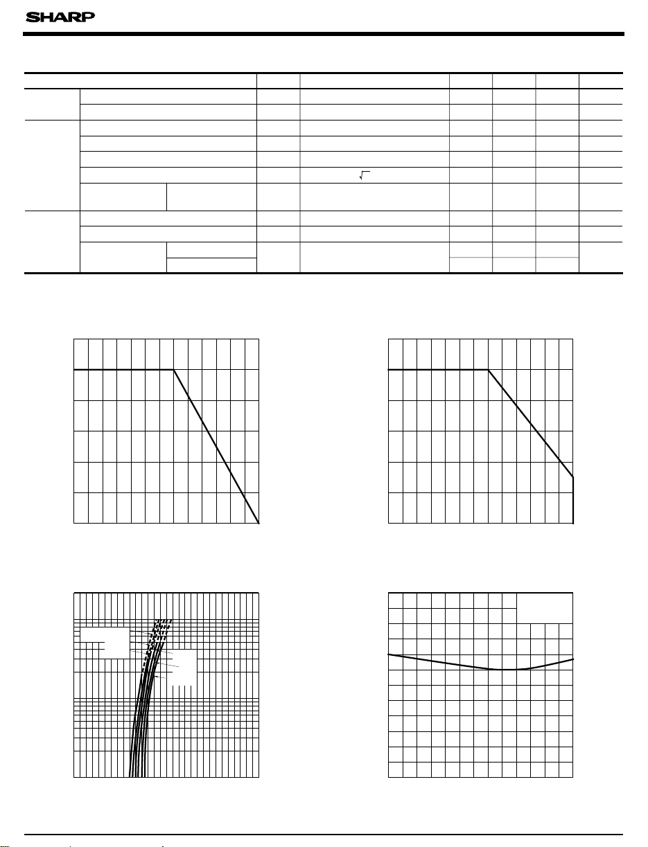
■ Electro-optical Characteristics
Parameter
Input
Output
Transfer
charac-
teristics
Fig. 1 RMS ON-state Current vs.
Ambient Temperature
)
mA
(
RMS ON-state current I
Forward voltage
Reverse current
Repetitive peak OFF-state current
ON-state voltage
Holding current
Critical rate of rise of OFF-state voltage
Zero-cross
voltage
Minimum trigger current
Isolation resistance
S11MS3/S21MS3
rms
T
Turn-on time
60
50
40
30
20
10
S21MS4
S21MS4
(
Ta= 25˚C
Symbol MIN. TYP. MAX. Unit
V
F
I
R
I
DRM
V
T
I
H
dV/dt
V
OX
I
FT
R
ISO
t
on
Conditions
= 20mA
I
F
=3V
V
R
= Rated
V
DRM
= 0.05A
I
T
=6V
V
D
= 1/ • Rated
DRM
2
V
IF= 15mA, Resistance load
= 6V, RL= 100Ω
V
D
DC500V, 40 to 60%RH
= 6V, RL= 100Ω ,
V
D
I
= 20mA
F
- 1.2 1.4 V
--10µA
--1µA
- - 2.5 V
0.1 - 3.5 mA
1 000
100 - V/µs
- - 35 V
- - 10 mA
5x101010
- - 100
--50
11
- Ω
µs
Fig. 2 Forward Current vs.
Ambient Temperature
60
50
)
mA
40
(
F
30
20
Forward current I
10
)
0
-
30 0 50 100
Ambient temperature Ta (˚C
Fig. 3 Forward Current vs.
Forward Voltage
200
100
T
= 100˚C
)
mA
(
F
Forward current I
a
50
20
10
75˚C
50˚C
5
2
1
0 0.5 1.0 1.5 2.5 3.02.0
Forward voltage VF (V
25˚C
0˚C
-30˚C
0
-
30
)
0 50 100
Ambient temperature Ta (˚C
)
Fig. 4-a Minimum Trigger Current vs.
Ambient Temperature
12
10
)
mA
(
8
FT
6
4
2
Minimum trigger current I
0
-
)
30
(S11MS3/S21MS3
V
R
Ambient temperature Ta (˚C
=6V
D
= 100Ω
L
)
)
100806040200
Page 3

S11MS3/S21MS3/S21MS4
Fig. 4-b Minimum Trigger Current vs.
Ambient Temperature
14
12
)
mA
(
10
FT
8
6
4
Minimum trigger current I
2
0
-
30
Ambient temperature Ta (˚C
(
S21MS4
VD=6V
= 100Ω
R
L
)
)
100806040200
Fig. 5-b Relative Repetitive Peak OFF-state
Voltage vs. Ambient Temperature
1.3
)
1.2
= 25˚C
j
1.1
T
(
DRM
1.0
/V
)
a
=T
0.9
j
T
(
0.8
DRM
Relative repetitive peak OFF-state voltage
V
0.7
- 30 020406080100
Ambient temperature Ta (˚C
(
S21MS4
)
)
Fig. 5-a Relative Repetitive Peak OFF-state
Voltage vs. Ambient Temperature
1.3
)
1.2
= 25˚C
i
1.1
T
(
DRM
1.0
/V
)
a
0.9
j
T=T
(
0.8
DRM
Relative repetitive peak OFF-state voltage
V
0.7
-
30
Ambient temperature T
(
S11MS3/S21MS3
0 20406080100
a
(˚C
)
)
Fig. 6 ON-state Voltage vs.
Ambient Temperature
2.0
1.8
)
V
(
1.6
T
1.4
1.2
ON-state voltage V
1.0
0.8
-
30 0 20 100
Ambient temperature Ta (˚C
S21MS4
I
= 50mA
T
S11MS3
S21MS3
40 60 80
)
Fig. 7-a Holding Current vs. Ambient Tem- Fig. 7-b Holding Current vs. Ambient Tem-
perature
10
5
)
mA
(
2
H
1
0.5
Holding current I
(
S11MS3/S21MS3
=6V
V
D
)
perature
10
)
5
mA
(
H
2
1
0.5
Holding current I
(
S21MS4
VD=6V
)
0.2
0.1
-
30 0 20406080100
Ambient temperature Ta (˚C
)
0.2
0.1
-
30
Ambient temperature T
a
(˚C
100
806040200
)
Page 4

S11MS3/S21MS3/S21MS4
Fig. 8-a Repetitive Peak OFF-state Current Fig. 8-b Repetitive Peak OFF-state Current
vs. OFF-state Voltage
2
)
A
(
-9
10
DRM
5
2
S11MS3
-10
10
Repetitive peak OFF-state current I
5
100 200 300 400 500 600
OFF-state voltage V
(
S11MS3
T
(V
D
)
= 25˚C
a
Fig. 9 Relative Repetitive Peak OFF-state
Current vs. Ambient Temperature
2
10
V
= 400V
DRM
)
1
10
= 25˚C
j
T
(
0
10
RM
/I
)
a
=T
j
T
-1
(
10
DRM
Relative repetitive peak OFF-state current
I
-2
10
-
30 0 10020 40 60 80
Ambient temperature T
a
(˚C
)
Fig.11 ON-state Current vs.
ON-state Voltage
100
= 20mA
I
F
90
T
= 25˚C
a
80
)
70
mA
(
60
T
50
40
30
ON-state current I
20
10
0
0 0.2 0.4 0.6 0.8 1.0 1.2 1.4 1.6 1.8 2.0
S11MS3
S21MS3
ON-state voltage V
S21MS4
)
(V
T
)
+V
vs. OFF-state Voltage
2
)
A
(
-9
10
DRM
5
2
-10
10
Repetitive peak OFF-state current I
5
100 200 300 400 500 600
(
S21MS3/S21MS4
S21MS4
S21MS3
OFF-state voltage V
T
)
(V
D
Fig.10 Zero-cross Voltage vs. Ambient
Temperature
30
)
V
(
25
OX
20
Zero-cross voltage V
15
-
30
Ambient temperature T
(
S21MS4
R load
= 15mA
I
F
)
(˚C
a
■Basic Operation Circuit
S11MS3/
S21MS3/S21MS4
CC
V
IN
16
3
Zerocross
Circuit
●
Please refer to the chapter
4
Zero-cross Circuit
(
S21MS4
AC100V
(
AC200V
(
“ Precautions for Use.”(Page 78 to 93).
)
= 25˚C
a
)
100806040200
Load
)
S11MS3
S21MS3/S21MS4
)
)
 Loading...