

Page 1
6-pin DIP Type SSR for Low
S11MA01/S21MA01
Power Control
S11MA01/S21MA01
■ Features
1. Low operating current type
(MAX 60mA
)
rms
2. Compact 5-pin dual-in-line package type
3. Recognized by UL file No. E94758
■ Applications
1. Electrical dampers for refrigerator
2. Turntable controllers for microwave oven
3. Ignitions circuit for oil fan heater
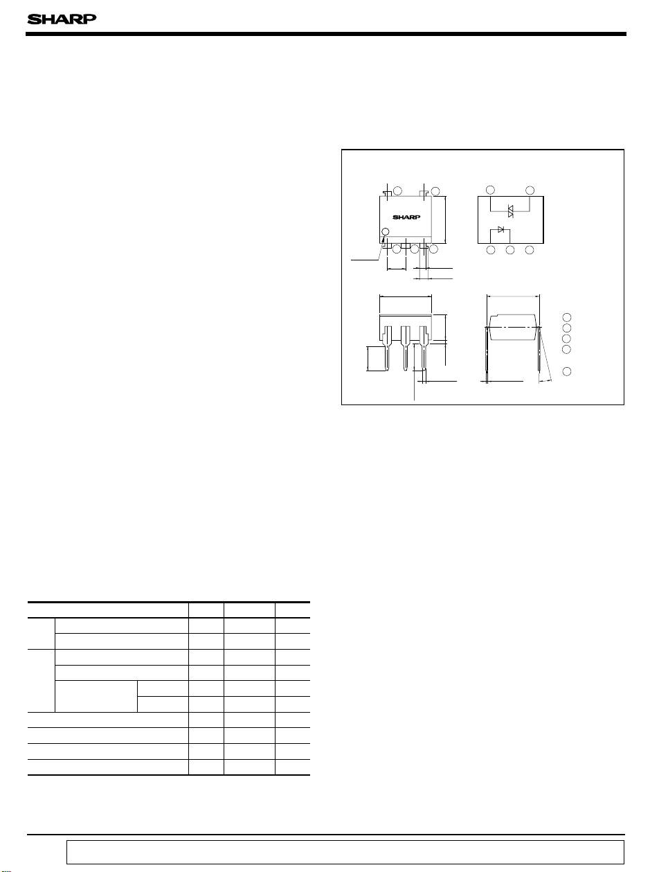
■ Outline Dimensions
S11MA01
Internal conection diagram
6
4
Anode
mark
0.5
±
3.35
S11MA01
12
±
0.25
2.54
7.12
±
0.5
±
3.7
0.5
±
6.5
3
±
0.2
0.9
±
0.3
1.2
0.5
0.5
±
3.5
TYP.
0.5
±
0.1
0.5
6
12
±
0.3
7.62
±
0.1
0.26
θ : 0 to 13 ˚
4
3
θ
(
Unit : mm
1 Anode
2 Cathode
3 NC
4 Anode,
Cathode
6 Anode,
Cathode
)
■ Absolute Maximum Ratings
Parameter
Forward current I
Input
Reverse voltage V
RMS ON-state current I
*1
Peak one cycle surge current
Output
Repetitive peak
OFF-state voltage
*2
Isolation voltage V
Operating temperature T
Storage temperature T
*3
Soldering temperature T
S11MA01
S21MA01
Symbol
F
R
T
I
surge
V
DRM
V
DRM
iso
opr
stg
sol
(
Ta= 25˚C
Rating Unit
50 mA
6V
100
1.2 A
400 V
600 V
5 000
- 25 to + 80
- 55 to + 125
260 ˚C
mA
V
)
rms
rms
˚C
˚C
*1 50Hz sine wave
*2 AC for 1 minute, 40 to 60%RH, f= 60Hz
*3 For 10 seconds
“ In the absence of confirmation by device specification sheets, SHARP takes no responsibility for any defects that occur in equipment using any of SHARP's devices, shown in catalogs,
data books, etc. Contact SHARP in order to obtain the latest version of the device specification sheets before using any SHARP's device.”
Page 2
S11MA01/S21MA01
■ Electro-optical Characteristics
Parameter
Input
Output
Transfer
charac-
teristics
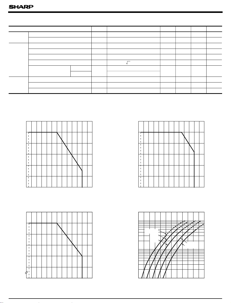
Fig. 1 RMS ON-state Current vs.
Forward voltage
Reverse current
Repetitive peak OFF-state voltage
ON-state voltage
Holding current
Critical rate of rise of OFF-state voltage
Operating current
Mininum trigger current
Isolation resistance
Turn-on time
Ambient Temperature
120
)
100
mArms
(
80
T
60
40
20
RMS ON-state current I
S11MA01
S21MA01
Symbol
I
V
F
F
I
V
R
I
V
DRM
V
I
T
T
I
V
H
V
dV/dt
AC100Vrms, 60Hz, Resistance load
AC200Vrms, 60Hz, Resistance load
V
I
FT
R
DC = 500V, 40 to 60% RH
ISO
t
VD= 6V, RL= 100Ω, IF= 20mA
on
Conditions
= 20mA
=3V
R
= Rated
DRM
= 0.06A
=6V
D
=(1/ )• Rated
DRM
D
2
= 6V, RL= 100 Ω
Fig. 2 Forward Current vs.
Ambient Temperature
)
mA
(
F
Forward current I
(
Ta= 25˚C
MIN.
500
5x10
60
50
40
30
20
10
TYP. MAX. Unit
1.2 1.4 V
-
-
-
-
0.1
-10
-10
- 2.5 V
1.0 3.5 mA
--V/µs
-
-
-
-60
-10mA
10
11
10
- 100 µs
-5
-6
- Ω
mA
)
A
A
rms
0
-30 -30
0 50 100
Ambient temperature Ta (˚C
)
Fig. 3 Operating Current vs.
Ambient Temperature
70
60
)
50
rms
mA
(
40
30
Operating current
20
0
-30
0 50 100
Ambient temperature T
a
(˚C
)
0
0 50 100
Ambient temperature T
Fig. 4 Forward Current vs.
Forward Voltage
100
)
50
T
= 75˚C
mA
(
F
Forward current I
a
50˚C
20
10
5
2
1
0.9 1.0 1.1 1.2 1.3 1.4 1.5
25˚C
Forward voltage V
F
(V
(˚C
a
)
0˚C
- 25˚C
)
Page 3
S11MA01/S21MA01
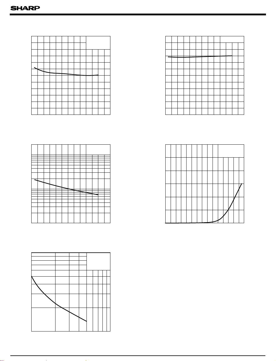
Fig. 5 Minimum Trigger Current vs.
Ambient Temperature
)
mA
(
FT
12
10
8
V
D
R
L
=6V
= 100Ω
6
4
Minimum trigger current I
2
0
- 30 0 20 40 60 80 100
Ambient temperature Ta (˚C
)
Fig. 7 Relative Holding Current vs.
Ambient Temperature
V
a
(˚C
D
)
100%
3
x
10
)
25˚C
(
H
/I
)
t˚C
(
H
2
10
Relative holding current I
1
10
- 30 0 20 40 60 80 100
Ambient temperature T
=6V
Fig. 6 ON-state Voltage vs.
Ambient Temperature
1.6
1.5
)
V
(
1.4
T
1.3
1.2
ON-state voltage V
1.1
1.0
- 30 0 20 40 60 80 100
Ambient temperature T
a
Fig. 8 ON-state Current vs.
ON-state Voltage
120
100
)
mA
80
(
T
60
40
ON-state current I
20
0
0 0.5 1.0 1.5
ON-state voltage V
(V
T
(˚C
I
T
= 0.06A
I
T
)
= 20mA
F
= 25˚C
a
)
Fig. 9 Turn-on Time vs. Forward Current
100
)
50
µ s
(
40
on
30
20
Turn-on time t
10
10
20 30 40 50 100
Forward current I
(mA
F
VD=6V
= 100Ω
R
L
= 20mA
I
F
)
Page 4
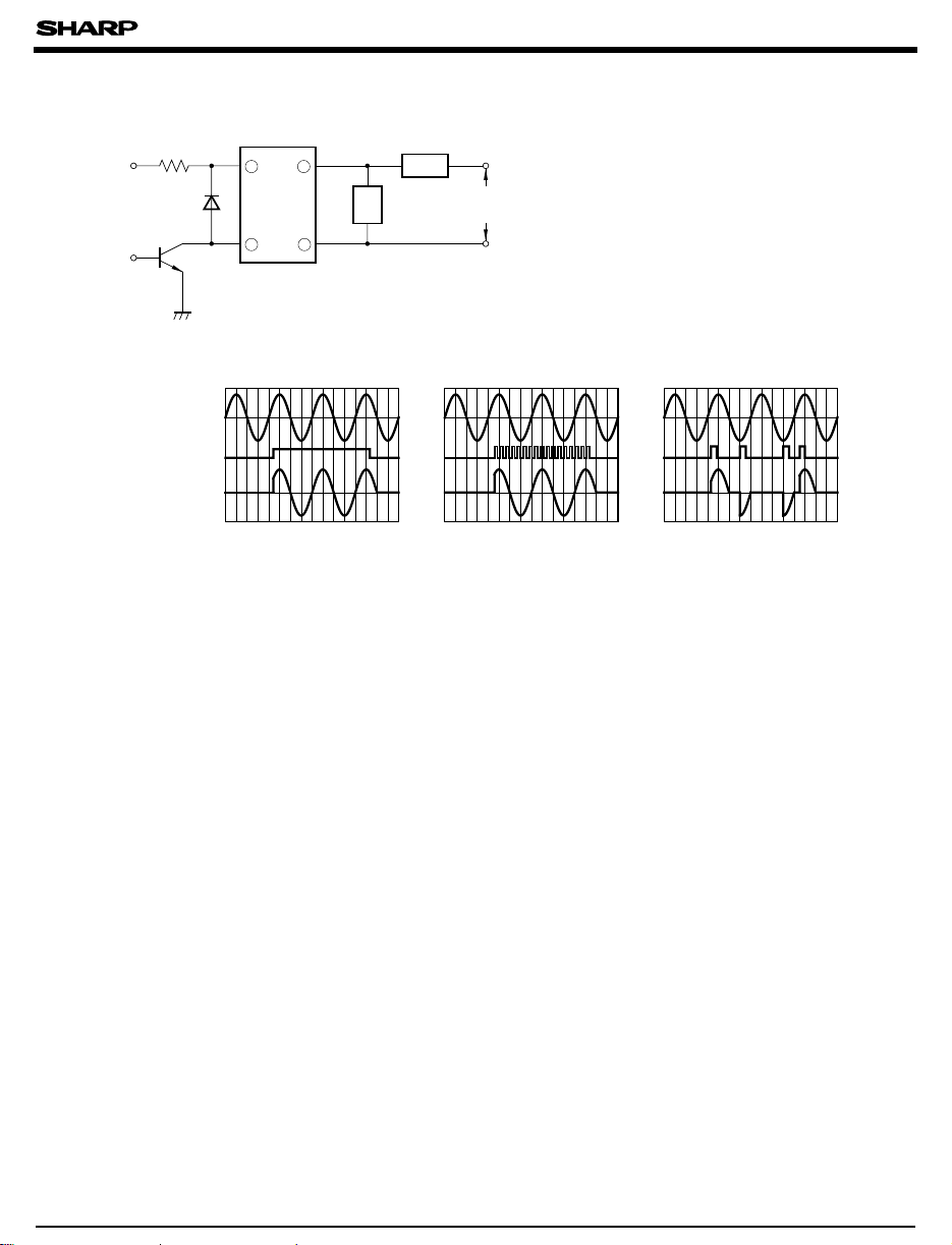
■ Basic Operation Circuit
R
+ V
CC
V
I
1
D
Tr1
1
1
SSR
2
6
4
ZS: Surge absorption circuit
Load
Z
S
AC 100V
AC 200V
S11MA01/S21MA01
(1)
DC Drive
AC supply voltage
Input signal
Load current
(
for resistance load
)
Notes 1) If large amount of surge is loaded onto V
or the driver circuit, add a diode D1 between terminals 1
CC
(2)
Pulse Drive
and 2 to prevent reverse bias from being applied to the infrared LED.
2) Be sure to install a surge absorption circuit.
An appropriate circuit must be chosen according to the load (for CR, choose its constant). This must be
carefully done especially for an inductive load.
3) For phase control, adjust such that the load current immediately after the input signal is applied will
be more than 10mA.
● Please refer to the chapter“ Precautions for Use”
(3)
Phase Control
 Loading...