

Page 1
S101S15V/S101S16V/S201S15V/S201S16V
S101S15V/S101S16V
S201S15V/S201S16V
■ Features
1. High radiation resin mold package
: MAX. 3A
I
T
2. Isolation voltage between input and output
: 3 000 V
V
iso
3. Built-in zero-cross circuit
(S101S16V/ S201S16V
4. Built-in snubber circuit
5. Recognized by UL, file No. E94758
Approved by CSA, file No. LR63705
■ Applications
1. Air conditioners
2. OA equipment
■ Model Line-ups
No built-in
zero-cross circuit
Built-in zero-cross
circuit
■ Absolute Maximum Ratings
Input
*1
Output
*2
*3
rms
rms
)
For 100V lines For 200V lines
S101S15V S201S15V
S101S16V S201S16V
(
Ta = 25˚C
Parameter
Symbol
Forward current I
Reverse current V
RMS ON-state current IT3 (Tc<=100˚C)A
Peak one cycle surge
current
Repetitive peak OFF-
state voltage
Critical rate of rise of
ON-state current
I
V
dIT/dt
Operating frequency f 45 to 65 H
Operating temperature T
Storage temperature T
Isolation voltage V
Soldering temperature T
100V line 200V line
F
R
surge
400 600 V
DRM
- 20 to + 80
opr
- 30 to +100
stg
iso
sol
Ratings
50 mA
6V
30 A
40
3.0
kV
260
Unit
A/µ s
˚C
˚C
˚C
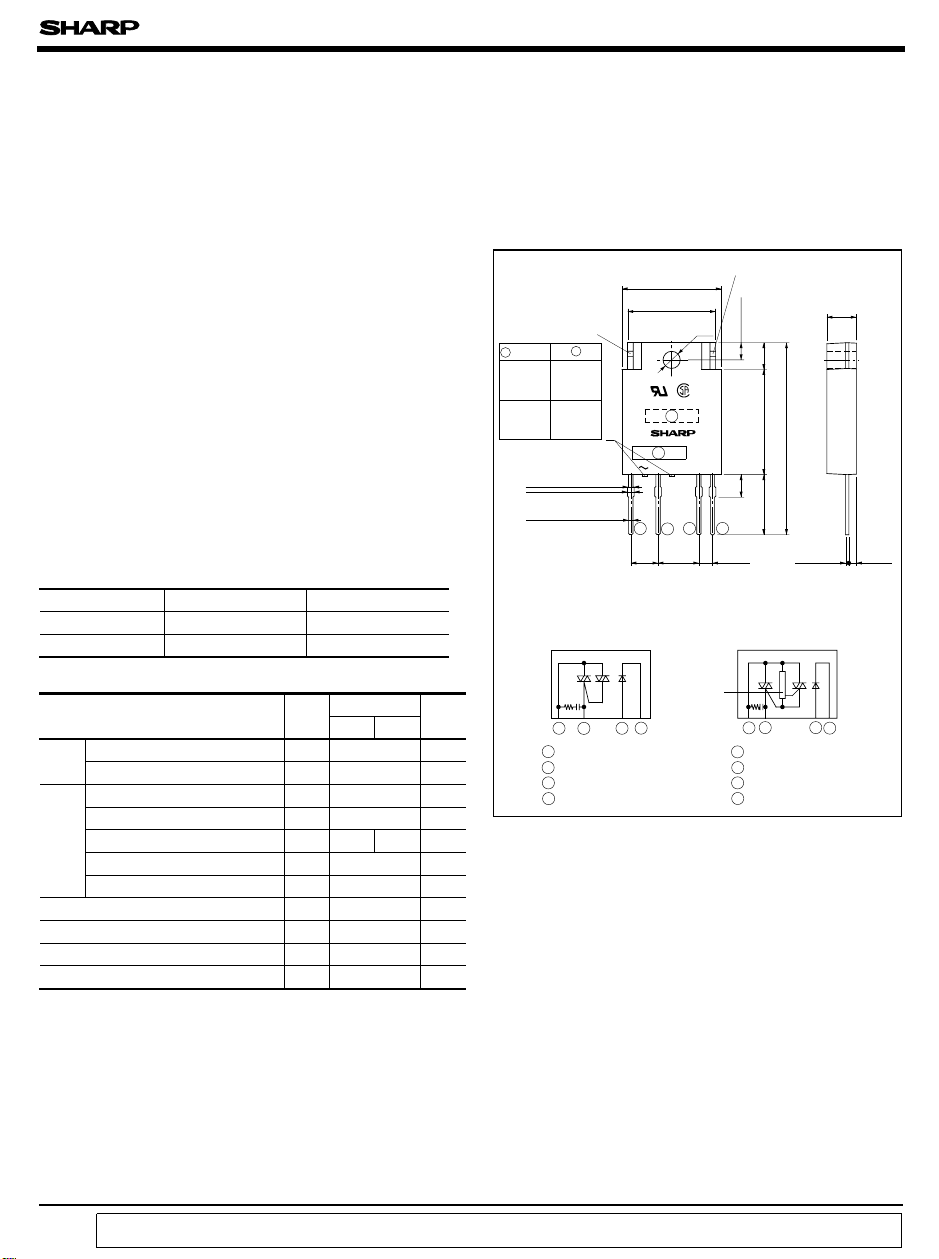
SIP Type SSR with Built-in
Snubber Circuit
■ Outline Dimensions
Common to Pin No.1
A Model No, B
S101S15V
3A125VAC
S101S16V
S201S15V
3A265VAC
S201S16V
±
0.2
4 - 1.1
±
4 - 1.25
±
0.2
4 - 0.8
Internal connection diagram
S101S15V/S201S15V S101S16V/S201S16V
)
1 Output (Triac T2
2 Output (Triac T1
rms
Z
rms
3 Input
4 Input
❈
0.3
(+)
(-)
±
0.2
18.5
±
0.3
16.4
±
0.2
φ 3.2
A
B
+
123 4
(
)
7.62
Zero-cross
circuit
)
)
)(
(
5.08
(
Common to Pin No.1
0.2
±
3.2
0.3
±
5.0
0.2
±
19.6
-
MIN.
MAX.
4.2
11.2
)
2.54
❈ May not be externally
connected
12 3412 34
1 Output (Triac T2
2 Output (Triac T1
(+)
3 Input
(-)
4 Input
Unit : mm
±
0.2
5.5
)
36.0
(
±
0.1
0.6
(
)
)
1.4
)
)
*1 60HZ sine wave, Tj= 25˚C
*2 AC 60Hz for 1 minute, 40 to 60%RH
Isolation voltage measuring method:
(1) Dielectric withstand tester, with zero-cross circuit shall be used.
(2) The waveform of applied voltage shall be sine wave.
(3) It shall be applied voltage between input and output.
(Input and output shall be short-circuited respectively
)
*3 For 10 seconds
“ In the absence of confirmation by device specification sheets, SHARP takes no responsibility for any defects that occur in equipment using any of SHARP's devices, shown in catalogs,
data books, etc. Contact SHARP in order to obtain the latest version of the device specification sheets before using any SHARP's device.”
Page 2
S101S15V/S101S16V/S201S15V/S201S16V
■ Electrical Characteristics
Parameter Symbol Condition MIN. TYP. MAX. Unit
Input
Output
Transfer
characteristics
Forward voltage V
Reverse current I
ON-state voltage V
Minimum oper-
ating current
Open circuit
leak current
S101S15V/16V
S201S15V/16V
S101S15V/16V
S201S15V/16V
Critical rate of rise of OFF-state voltage
Commutation critical rate of rise
of OFF-state voltage
Minimum trig-
ger current
S101S15V/S201S15V
S101S16V/S201S16V
Isolation resistance DC500V, R
Zero-cross
voltage
Turn-on time
S101S16V
S201S16V --35
S101S15V/S201S15V
S101S16V/S201S16V
Turn-off time toff AC50H
Thermal resistance
Thermal resistance
Between junction and case
Between junction and ambient
F
R
T
I
OP
I
leak
dV/dt
(
dV/dt)c
I
FT
R
ISO
V
OXIF
ton AC50H
)
R
th (j-c
)
R
th (j-a
(
Ta= 25˚C
IF= 20mA - 1.2 1.4 V
VR=3V - - 10
Resistance load, IF= 20mA,
IT= 1.5A
V
V
V
V
VD= 2/3V
OUT
OUT
OUT
OUT
rms
= 120V
= 240V
= 120V
= 240V
rms
rms
rms
rms
DRM
Tj= 125˚C, VD= 400V,
dIT/dt= -1.5A/ms
VD= 12V, RL=30Ω
VD= 6V, RL=30Ω
= 40 to 60% 10
H
= 15mA
Z
Z
-
- 45 - ˚C/W
- - 1.5 V
- - 50 mA
--5
--10
30 - -
4--
- - 15 mA
10
--Ω
--35
--1
--10
--10
- 6 - ˚C/W
-
-4
mA
V/µ s
V/µ s
)
A
rms
rms
rms
V
ms
ms
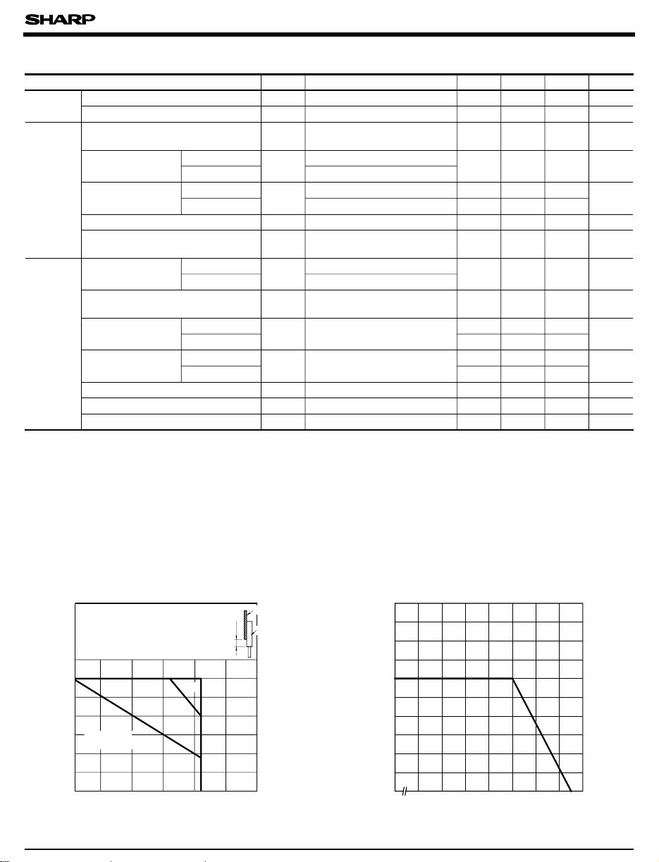
Fig. 1 RMS ON-state Current vs.
Ambient Temperature
(1)
With heat sink(Al 100x100
(2)
With heat sink(Al 50x 50
5
Note) With the Al heat sink set up vertically,
install it as shown in the figure
Torque : 4kg•cm
)
Apply thermal conductive silicone grease
4
on the heat sink mounting plate.forcibly
rms
A
cooling shall not be carried out.
(
T
3
2
Without
heat sink
1
RMS ON-state current I
0
0 25 50 100 125
-20 7580
Ambient temperature Ta (˚C
(2)
t
x
)
2mm
t
x
)
2mm
Al plate
SSR
5mm
(1)
)
Fig. 2 RMS ON-state Current vs.
Case Temperature
5
)
4
rms
A
(
T
3
2
1
RMS ON-state current I
0
60 70 80 90 100 110 120 130
-20
Case temperature T
c
(˚C
125
)
Page 3

S101S15V/S101S16V/S201S15V/S201S16V
Fig. 3 Forward Current vs.
Ambient Temperature
60
50
)
mA
(
40
F
30
20
Forward current I
10
0
-20
05080
Ambient temperature Ta (˚C
)
Fig. 5 Surge Current vs. Power-on cycle
60
50
)
A
(
40
surge
30
20
Surge current I
10
0
1 100
Power-on cycle (times
f= 60H
Tj= 25˚Cstart
10
z
)
Fig. 7-a Minimum Trigger Current vs.
Ambient Temperature (Typical Value
(
S101S15V/S201S15V
= 12V
V
D
R
=30Ω
L
)
mA
(
FT
12
10
8
100
)
Fig. 5 Forward Current vs. Forward Voltage
200
100
50
)
mA
(
F
20
10
Forward current I
= 75˚C
T
a
50˚C
5
2
1
0.5 1.0 1.5 2.0 2.5 3.0
0
Forward voltage VF (V
25˚C
0˚C
)
Fig. 6 Maximum ON-state Power Dissipation vs.
RMS ON-state Current (Typical Value
6
)
W
(
5
4
3
2
1
Maximum ON-state power dissipation
0123456
RMS on-state current IT (A
T
a
rms
)
= 25˚C
)
Fig. 7-b Minimum Trigger Current vs.
)
Ambient Temperature (Typical Value
(
S101S16V/S201S16V
=6V
V
D
R
=30Ω
L
)
mA
(
12
10
FT
8
)
)
6
4
2
Minimum trigger current I
0 25 50 75 100 125
-20
Ambient temperature Ta (˚C
6
4
Minimum trigger current I
2
0 25 50 75 100 125
)
-20
Ambient temperature Ta (˚C
)
Page 4

S101S15V/S101S16V/S201S15V/S201S16V
Fig. 8-a Open Circuit Leak Current vs. Supply
(
V
)
Ta= 25˚C
)
rms
)
Voltage (Typical Value
)
5
rms
mA
(
4
leak
3
2
1
Open circuit leak current I
0
0 100 160
(
S101S15V, S101S16V
Supply voltage
● Please refer to the chapter “ Precautions for Use.”
Fig. 8-b Open Circuit Leak Current vs. Supply
Voltage (Typical Value
(S201S15V, S201S16V
)
rms
5
mA
(
leak
4
3
2
Open circuit leak current I
1
0
0 200 320
Supply voltage (V
)
)
= 25˚C
T
a
)
rms
 Loading...