

Datasheet RV5VE001A-E1, RV5VE001A-E2, RV5VE001B-E1, RV5VE001B-E2, RV5VE001C-E1 Datasheet (RICOH)
...Page 1

MULTI-POWER SUPPLY
RV5VE0××× SERIES
APPLICATION MANUAL
NO.EA-021-0006
Page 2
MULTI-POWER SUPPLY
1
RV5VE0
×××
SERIES
OUTLINE
The RV5VE0×××series are multi-power supply ICs with high accuracy output voltage and detector threshold
and with ultra low supply current by CMOS process. Each of these ICs consists of four voltage regulators,two voltage detectors and control switches.These ICs can achieve the construction of an ideal power supply system in
accordance with the user's mask option.
Output Voltage and Detector Threshold can be independently set within each IC by laser trim. The package
are of 16pin SSOP(0.8mm pitch) and 16pin SSOP(0.65mm pitch).
•
Ultra-Low Supply Current
•
Broad Operating Voltage Range
.....................
1.5V to 10.0V
•
High Accuracy Output Voltage and Detector Threshold
.....................................................
±
2.5%
•
Output Voltage and Detector Threshold
........
Stepwise setting with a step of 0.1V is possible
(refer to Selection Guide)
•
Low Temperature-Drift Coefficients of Output Voltage and Detector Threshold
.............
TYP. ±100ppm/˚C
•
Small Dropout Voltage
.....................................
50mV when IOUT is 80mA (Regulators 1, 2)
•
Small Package
..................................................
16pin SSOP (0.8mm pitch)
16pin SSOP (0.65mm pitch)
•
Direct connection to CPU is possible by an internal Level Shift Circuit.
FEATURES
APPLICATIONS
•
Power source system for hand-held communication equipment such as cellular phones and cordless telephones.
•
Power source system for battery-powered appliances.
PIN CONFIGURATION
•
RV5VE001
×
VSEN2
CD
RESET
D
OUT
IBC1
GND
V
DD
CSW3
ROUT2
IBC2
ROUT1
2
V
SEN1
CSW2
CSW1
R
OUT4 1
3
4
6
8
5
7
9
10
11
16
15
13
14
12
R
OUT3
Page 3
2
Part Number is designated as follows :
RV5VE0
×××– ××
← Part Number
↑↑↑↑↑
abcde
SELECTION GUIDE
In the RV5VE0×××series, Standard ICs and Customized ICs by mask option (hereinafter Optional Mask
Version ICs) are available at the user's request. Voltage settings for six circuits, four for Regulators and two for
Detectors, can be designated.
}
Code Contents
a
Designation of Package Type:
V : 16pin SSOP (0.65mm pitch)
b Serial Number for Multi-Power Supply IC (RV5VE) series:
Serial Number for Mask Version:
c
×1 for Standard ICs. Other numbers for Optional Mask Version ICs.
d
Serial Number for Voltage Setting:
A to Z are assigned in alphabetical order. (except I,O,Q,X)
Designation of Taping Type:
e
Ex. E1, E2
(refer to Taping Specifications)
RV5VE0×××
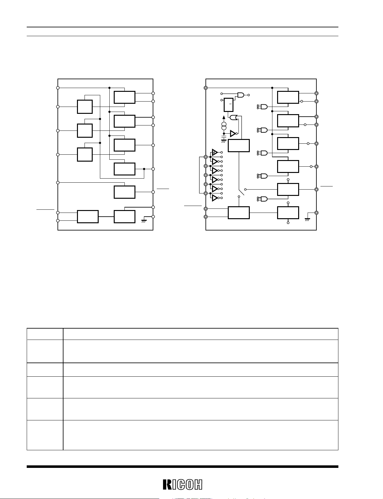
BLOCK DIAGRAMS
CSW1
V
SEN1
RESET
C
D
GND
V
SEN2
Level
Shift
ROUT1
IBC1
Regulator
2
CSW2
CSW3
I
BC2
ROUT2
ROUT3
ROUT4
DOUT
Level
Shift
Level
Shift
Regulator
1
Regulator
3
Detector
2
Detector
1
Delay
Generator
VDD
Regulator
4
•
RV5VE001
×
VDD
Detector
2
CD
GND
D
OUT
Regulator
1
ROUT1
IBC1
RESET
R
OUT2
IBC2
ROUT3
ROUT4
Regulator
2
Regulator
3
Regulator
4
Detector
1
Delay
Generator
T
Q
Q
R
One Shot
Pulse
Generator
to be named by uesr
•
RV5VE0
×××
(Optional Mask Version)
}
Page 4
3
PIN DESCRIPTION
Pin No. Symbol
1ROUT4
2VSEN2
3CD
4 RESET
5DOUT
6ROUT1
7IBC1
8 GND
9IBC2
10 ROUT2
11 CSW1
12 CSW2
13 CSW3
14 VSEN1
15 ROUT3
16 VDD
Description
Output Pin for Voltage Regulator 4.
Sense Pin for Voltage Detector 2.
Pin for External Capacitor for Delay Time Setting of Voltage Detector 2.
Output Pin of Voltage Detector 2. Nch Open Drain Output. “L” Outputat Detection.
Output Pin of Voltage Detector 1. Nch Open Drain Output. “L” Output at Detection.
Output Pin of Voltage Regulator 1. Connected to Collector of PNP Transistor.
Connected to Base of External PNP Transistor for Voltage Regulator 1 and controls Base Current.
Ground Pin.
Connected to Base of External PNP Transistor for Voltage Regulator 2 and controls Base Current.
Output Pin of Voltage Regulator 2. Connected to Collector of PNP Transistor.
Control Switch Input Pin for turning Voltage Regulator 1 ON/OFF.
Input level for this Input Pin is Active “H” .
Control Switch Input Pin for turning Voltage Regulator 2 ON/OFF.
Input level for this Input Pin is Active “H”
Control Switch Input Pin for turning Voltage Regulator 3 ON/OFF.
Input level for this Input Pin is Active “H” .
Sense Pin of Voltage Detector 1.
Output Pin of Voltage Regulator 3.
V
DD Pin.
• RV5VE001×(Standard ICs)
• RV5VE0×××(Optional Mask Version ICs)
Pin No. Symbol
2
11
12
13
14
Description
5 Pins Nos. 2, 11, 12, 13 and 14 can be designated as Input Pins by User's
choice. Refer to Optional Mask Version Guide.
Pins other than the above 5 Pins can be selected from the same pins as those
used in R
×5VE001×(Standard ICs)
To be
named
by User
RV5VE0×××
Page 5
4
OPTIONAL MASK VERSION GUIDE
User can designate an optional mask version in accordance with the following Optional Mask Version Guide:
•
Functions of Input Pins by User' Choice
Pin No. Symbol
2
11
12
13
14
Functions
Control Switch of Each Circuit, Sense Pin of Voltage Detector 1 or 2.
Control Switch of Each Circuit, Schmitt trigger input possible.
Control Switch of Each Circuit only.
Control Switch of Each Circuit only.
Control Switch of Each Circuit, Sense Pin of Voltage Detector 1 or 2.
To be
named
by User
Item
Sense Pins of Voltage
Detectors 1, 2
ON/OFF Control of
Regulators and
Detectors
ON/OFF Control by
Toggle Input
(only Pin 11)
Pins by User's Choice
Output of Voltage
Detectors 1, 2
Description
•
sense Pins of Voltage Detectors 1, 2 can be connected to Output ROUT1, ROUT2,
R
OUT
3
, ROUT4of Voltage Regulators, or VDD.
•
ON/OFF Control of Voltage Regulators 1 to 4 and Voltage Detector 1 can be per-
formed by 3 INPUT AND Gate.
•
ON/OFF Control of Voltage Detector 2 can be directly performed.
•
ON/OFF Control of 4 Voltage Regulators and 2 Voltage Detectors can be per-
formed by AND Gate of Toggle Input and Level Input.
•
Edge Trigger Flip-Flop (Rise Edge Operation) is reset and Initialized at the rise
of power source or at the detection operation of Voltage Detector 1 or 2.
•
Flip-Flop can be reset by one shot pulse at the detection of Voltage Detector 1 or
2, or the reset state can be maintained during the detection operation.
•
Five Input Pins are available as User's Pins as shown in the TABLE shown below.
•
ON/OFF Control Input Pins for Regulators and detectors.
•
Sense Pins of Voltage Detectors 1,2.
•
Active “H” Input or Active “L” Input can be selected.
•
RESET Output and DOUT Output, which are output from Voltage Detectors 1, 2,
can be set at “L” or “H” at the time of the detection.
•
RESET Output and DOUT Output, which are output from Voltage Detectors 1,
2,can be set at “L” or “H” at the time of OFF by ON/OFF Control.
•
Output Signals of Voltage Detectors 1, 2 can perform ON/OFF control of Voltage
Regulators 1 to 4.
RV5VE0×××
Page 6

5
RV5VE0×××
DESCRIPTION OF EACH CIRCUIT
1. Voltage Regulators 1,2
•
Voltage Regulators 1, 2 are linear regulators which can be constructed of external PNP Transistor, and are capa-
ble of obtaining a large output current by a small Dropout Voltage.
•
Output Voltage of each of Voltage Regulators 1, 2 can be set stepwise with a step of 0.1V in the range of 3V to 6V
by laser trim.
•
Voltage Regulators 1, 2 can be turned ON/OFF by Control Pins.
•
Use External PNP Transistor of a low saturation type, with an hFE of 100 or more.
•
Use Voltage Regulators 1, 2 with the attachment of a Capacitor with a capacitance of 10µF or more to the Output
Pins.
2. Voltage Regulators 3,4
• Voltage Regulators 3, 4 are CMOS type linear regulators and have the same structure as those of Voltage
Regulators R
×5RL and R×5RE series.
• Output Voltage of each of Voltage Regulators 3, 4 can be set stepwise with a step of 0.1V in the range of 2V to 6V
by laser trim.
• Voltage Regulators 3, 4 can be turned ON/OFF by Control Pins.
3. Voltage Detector 1
• When Voltage Detector 1 detects the lowering of VSEN1, the level of the output of Voltage Detector 1 becomes “L”
level. The output of Voltage Detector 1 is Nch Open Drain Output.
• Voltage Detector 1 can be set as follows by optional mask:
1. ON/OFF Control of Voltage Detector 1.
2. Output of Voltage Detector 1 at the detection can be set at “L” level or “H” level.
3. Output of Voltage Detector 1 at OFF can be set at “L” level or “H” level.
4. Sense Pins of Voltage Detectors 1, 2 can be connected to Output R
OUT1, ROUT2, ROUT3, ROUT4 of Voltage
Regulators or V
DD within the IC.
4. Voltage Detector 2
•
When Voltage Detector 2 detects the lowering of VSEN2, the level of the output of Voltage Detector 2 becomes “L”
level. The output of Voltage Detector 2 is Nch Open Drain Output.
•
Voltage Detector 2 can set Reset Delay Time. Delay Time can be set in accordance with the capacitance CD of
External Capacitor as shown on the following pages.
•
Voltage detector 2 can be set as follows by optional mask:
1. ON/OFF Control of Voltage Detector 2.
2. Output of Voltage Detector 2 at the detection can be set at “L” level or “H” level.
3. Output of Voltage Detector 2 at OFF can be set at “L” level or “H” level.
4. Sense Pins of Voltage Detectors 2 can be connected to Output R
OUT1, ROUT2, ROUT3, ROUT4 of Voltage
Regulators or V
DD within the IC.
Page 7
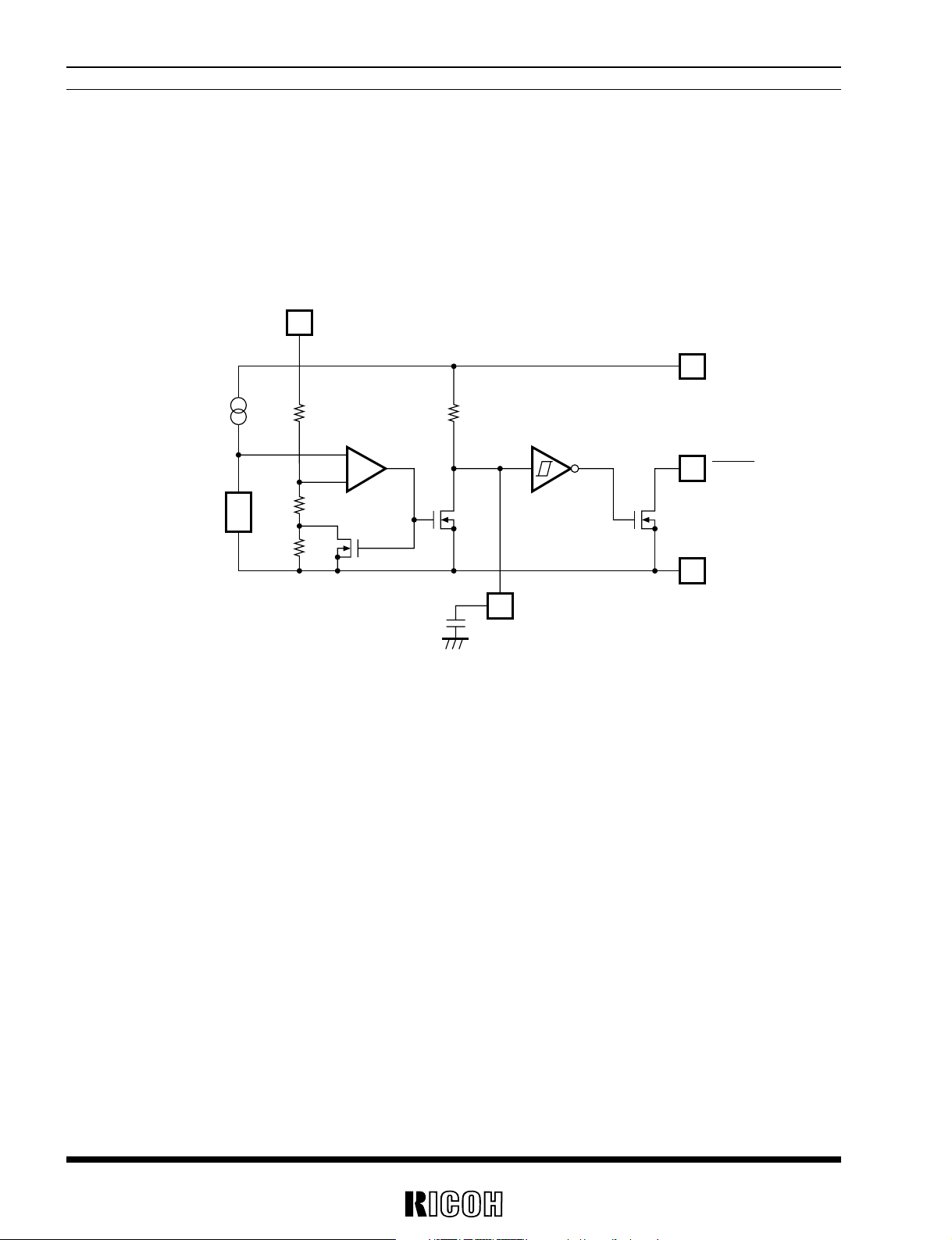
6
Current Source
Extermal Capacitor
R
D
GND
V
DD
RESET
V
SEN2
CD
Vref
+
–
5. Main Power Source Control (in the case of Optional Mask Version)
• This IC includes built-in Edge Trigger Flip-Flop (Rising Edge Operation) and AND Gate, so that Main Power
Source of any instruments can be turned ON/OFF by “AND” of Toggle Input and Level Input.
• Edge Trigger Flip-Flop is reset by One Shot Pulse Generator when Voltage Detector 1 or 2 detects the lowering
of the voltage. This Flip-Flop can be continuously reset during the detection.
RV5VE0×××
• Formula for calculating Reset Delay Time is
tD = 0.69 ×RD ×CD
wherein RD is the resistance of a built-in resistor and can be set at 1MΩ in IC, so that the above formula is:
tD = 0.69 ×10
6
×CD
Voltage Detector with Delay Circuit is constructed as shown below.
• Block Diagram of Voltage Detector with delay Circuit.
Page 8
7
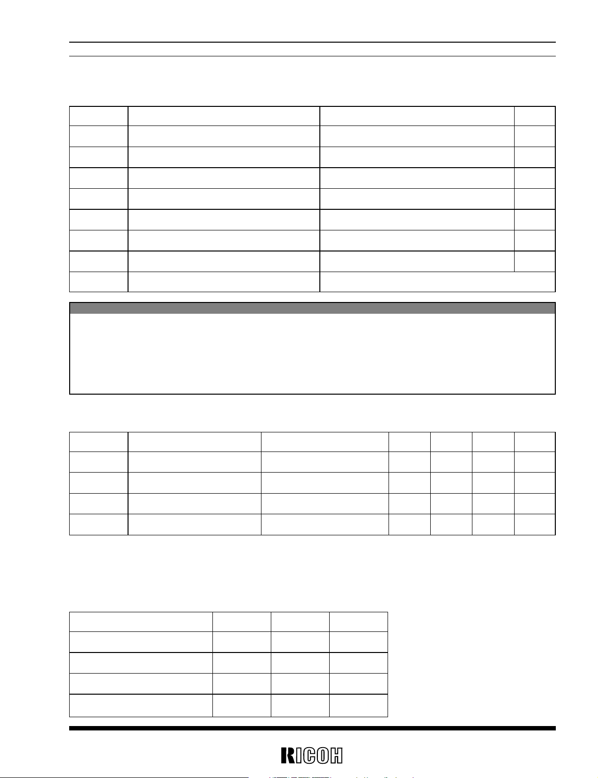
• Electrical Characteristics of R×5VE001×
Symbol Item
VIN Input Voltage
VOUT Output Voltage
IOUT Output Current
PD1
Power Dissipation1 (16pin SSOP (0.8mm pitch))
PD2
Power Dissipation2 (16pin SSOP (0.65mm pitch))
Topt Operating Temperature Range
Tstg Storage Temperature Range
Tsolder Lead Temperature(Soldering)
Rating Unit
+12 V
–0.3 to VIN+0.3 V
300 mA
500 mW
470 mW
–30 to +80 ˚C
–40 to +125 ˚C
260˚C 10s
ABSOLUTE MAXIMUM RATINGS
OVERALL CHARACTERISTICS
Symbol Item
VDD Operationg Voltage Range
ROUT1,2
Output Voltage Setting Range 1
ROUT3,4
Output Voltage Setting Range 2
–VDET
Detector Threshold Setting Range
Conditions MIN. TYP. MAX. Unit
1.5 10.0 V
Step of 0.1V 3.0 6.0 V
Step of 0.1V 2.0 6.0 V
Step of 0.1V 2.0 6.0 V
The following three types of ICs are available as Standard ICs.The details of these ICs are shown in the section
of Electrical Characteristics on the following pages:
•
List of Standard Voltage Settings
Type Number R×5VE001A R×5VE001B R×5VE001C
Output Voltage of Regulator 1 to 4 5.0V 4.0V 3.0V
Threshold Voltage of Detector 1 5.4V 4.4V 3.4V
Threshold Voltage of Detector 2 4.5V 3.5V 2.5V
Conditions for Input Voltage 6.0V 4.8V 3.6V
RV5VE0×××
Absolute Maximum ratings are threshold limit values that must not be exceeded even for an instant under any
conditions. Moreover, such values for any two items must not be reached simultaneously. Operation above
these absolute maximum ratings may cause degradation or permanent damage to the device. These are stress
ratings only and do not necessarily imply functional operation below these limits.
ABSOLUTE MAXIMUM RATINGS
Page 9
8
• RV5VE001A
(Note 1) Unless otherwise provided, VDD = 6.0V, IOUT = 50mA, Co = 10µF, Rbe = 100kΩ.
(Note 2) Use External Transistor with h
FE ≥ 100.
(Note 3) Quiescent Current = Operating Current of Regulators 1, 2 + 0.6/Rbe.
(Note 4) Supply Current = Quiescent (No Load) Current + Load Current/h
FE.
Symbol Item
ROUT1,2 Output Voltage
ISS1,2 Quiescent Current
Iopr1,2 Supply Current
VDIF1,2 Dropout Voltage
∆V
OUT
Load Regulation
∆IOUT
∆VOUT
Line Regulation
∆VIN
RR Ripple Rejection
I
lim1,2 Current Limit
∆VOUT Output Voltage
∆Topt Temperature Coefficient
Conditions MIN. TYP. MAX. Unit
4.875 5.000 5.125 V
IOUT=0mA 100 µA
IOUT=80mA 1 mA
ROUT1,2=5.0V,IOUT=80mA 0.05 0.3 V
R
OUT1,2=5.0V
1mA≤IOUT≤80mA
50 mV
R
OUT1,2+0.3V≤VIN≤10.0V 0.05 0.3 %/V
f=120HZ,Ripple 0.5Vrms 40 60 dB
Base Current of I
B1,2of
310mA
PNP Transistor
±100 ppm/˚C
Topt=25˚C
Voltage Regulator 3 [RV5VE001A]
Symbol Item
ROUT
3
Output Voltage
ISS3 Supply Current
VDIF3 Dropout Voltage
∆V
OUT
Load Regulation
∆IOUT
∆VOUT
Line Regulation
∆VIN
Ilim3 Current Limit
∆V
OUT
Output Voltage
∆Topt
Temperature Coefficient
Conditions MIN. TYP. MAX. Unit
4.875 5.000 5.125 V
5.0 10.0 µA
ROUT3=5.0V,IOUT=50mA 0.3 V
R
OUT
3
=5.0V
1mA≤IOUT≤50mA
50 mV
R
OUT3+0.5V≤VIN≤10.0V 0.05 0.3 %/V
100 300 mA
±100 ppm/˚C
Topt=25˚C
Voltage Regulators 1, 2 [ RV5VE001A]
(Note) Unless otherwise provided, VDD = 6.0V, IOUT = 30mA
RV5VE0×××
Page 10
9
RV5VE0×××
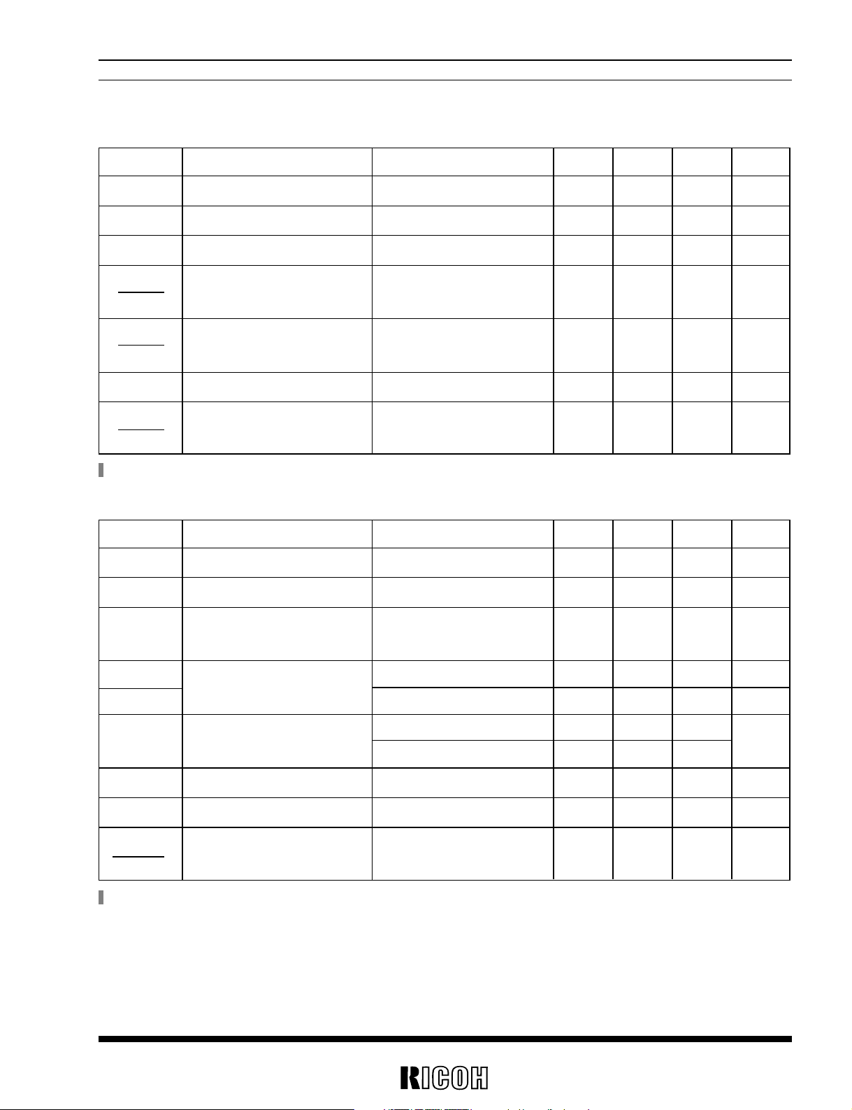
Voltage Regulator 4 [RV5VE001A]
Topt=25˚C
(Note) Unless otherwise provided, VDD = 6.0V, IOUT = 10mA
Voltage Detectors 1,2 [RV5VE001A]
Symbol Item
–VDET1 Detector Threshold 1
–VDET2 Detector Threshold 2
V
HYS Detector Threshold Hysteresis
ISS5
ISS6
Supply Current
I
OUT Output Current
RD Output Delay Resistor
ISEN Sense Pin Input Current
∆V
DET Detector Threshold
∆Topt Temperature Coefficient
Conditions MIN. TYP. MAX. Unit
Voltage Detector 1 5.265 5.400 5.535 V
Voltage Detector 2 4.388 4.500 4.612 V
(–V
DET)
×
0.05
V
Voltage Detector 1,VDD=6.0V 1.3 3.9 µA
Voltage Detector 2,VDD=6.0V 1.5 4.5 µA
V
DS=0.5V, VDD=1.5V 1.5
mA
VDS=0.5V, VDD=6.0V 11.6
Voltage Detector 2 only 0.5 1.0 2.0 MΩ
VSEN=6.0V 0.5 2 µA
±100 ppm/˚C
Topt=25˚C
(Note) Unless otherwise provided, VDD = 6.0V.
Symbol Item
ROUT4 Output Voltage
ISS4 Supply Current
VDIF4 Dropout Voltage
∆V
OUT
Load Regulation
∆IOUT
∆VOUT
Line Regulation
∆VIN
Ilim4 Current Limit
∆V
OUT
Output Voltage
∆Topt
Temperature Coefficient
Conditions MIN. TYP. MAX. Unit
4.875 5.000 5.125 V
1.3 3.9 µA
ROUT4=5.0V,IOUT=20mA 0.3 V
R
OUT
4
=5.0V
1mA≤IOUT
≤
20mA
50 mV
R
OUT4+0.5V≤VIN≤10.0V 0.05 0.3 %/V
100 300 mA
±100 ppm/˚C
Page 11
10
Input Pins [RV5VE001A]
Symbol Item
Ileak Input Leakage Current
V
IL
Control Switch
Low Level Input Voltage
V
IH
Control Switch
High Level Input Voltage
V
SIL
Schmitt Trigger
Low Level Input Voltage
V
SIH
Schmitt Trigger
High Level Input Voltage
V
HYS
Schmitt Trigger
Hysteresis Voltage
Conditions MIN. TYP. MAX. Unit
–1 1 µA
CSW1 to 4 0 0.8 V
CSW1 to 4 2.4 VDD V
Optional V
Optional V
Optional V
Topt=25˚C
(Note) Unless otherwise provided, VDD = 6.0V.
RV5VE0×××
Page 12
11
• RV5VE001B
(Note 1) Unless otherwise provided, VDD = 4.8V, IOUT = 50mA, Co = 10µF, Rbe = 100kΩ.
(Note 2) Use External Transistor with h
FE ≥ 100.
(Note 3) Quiescent Current = Operating Current of Regulators 1, 2 + 0.6/Rbe.
(Note 4) Supply Current = Quiescent (No Load) Current + Load Current/h
FE.
Voltage Regulator 3 [RV5VE001B]
Voltage Regulators 1, 2 [RV5VE001B]
(Note) Unless otherwiseprovided, VDD = 4.8V, IOUT = 30mA.
Topt=25˚C
Topt=25˚C
RV5VE0×××
Symbol Item
ROUT1,2 Output Voltage
ISS1,2 Quiescent Current
Iopr1,2 Supply Current
VDIF1,2 Dropout Voltage
∆V
OUT
Load Regulation
∆IOUT
∆VOUT
Line Regulation
∆VIN
RR Ripple Rejection
I
lim1,2 Current Limit
∆VOUT Output Voltage
∆Topt Temperature Coefficient
Conditions MIN. TYP. MAX. Unit
3.900 4.000 4.100 V
IOUT=0mA 100 µA
IOUT=80mA 1 mA
ROUT1,2=4.0V,IOUT=80mA 0.05 0.3 V
R
OUT
1,2
=4.0V
1mA≤IOUT≤80mA
50 mV
R
OUT1,2+0.3V≤VIN≤10.0V 0.05 0.3 %/V
f=120HZ,Ripple 0.5Vrms 40 60 dB
Base Current of I
B1,2of
310mA
PNP Transistor
±100 ppm/˚C
Symbol Item
ROUT
3
Output Voltage
ISS
3
Supply Current
VDIF3 Dropout Voltage
∆V
OUT
Load Regulation
∆IOUT
∆VOUT
Line Regulation
∆VIN
Ilim3 Current Limit
∆V
OUT
Output Voltage
∆Topt
Temperature Coefficient
Conditions MIN. TYP. MAX. Unit
3.900 4.000 4.100 V
5.0 10.0 µA
ROUT3=4.0V,IOUT=43mA 0.3 V
R
OUT
3
=4.0V
1mA≤IOUT≤43mA
50 mV
R
OUT3+0.5V≤VIN≤10.0V 0.05 0.3 % /V
100 300 mA
±100 ppm/˚C
Page 13
12
Voltage Regulator 4 [RV5VE001B]
Topt=25˚C
(Note) Unless otherwise provided, VDD = 4.8V, IOUT = 10mA
Voltage Detectors 1,2 [RV5VE001B]
Topt=25˚C
(Note) Unless otherwise provided, VDD = 4.8V.
RV5VE0×××
Symbol Item
ROUT4 Output Voltage
ISS4 Supply Current
VDIF4 Dropout Voltage
∆V
OUT
Load Regulation
∆IOUT
∆VOUT
Line Regulation
∆VIN
Ilim4 Current Limit
∆V
OUT
Output Voltage
∆Topt
Temperature Coefficient
Conditions MIN. TYP. MAX. Unit
3.900 4.000 4.100 V
1.3 3.9 µA
ROUT4=4.0V,IOUT=17.5mA 0.3 V
R
OUT
4
=4.0V
1mA≤IOUT
≤
17.5mA
50 mV
R
OUT4+0.5V≤VIN≤10.0V 0.05 0.3 %/V
100 300 mA
±100 ppm/˚C
Symbol Item
–VDET1 Detector Threshold 1
–VDET2 Detector Threshold 2
V
HYS Detector Threshold Hysteresis
ISS5
ISS6
Supply Current
I
OUT Output Current
RD Output Delay Resistor
ISEN Sense Pin Input Current
∆V
DET Detector Threshold
∆Topt Temperature Coefficient
Conditions MIN. TYP. MAX. Unit
Voltage Detector 1 4.290 4.400 4.510 V
Voltage Detector 2 3.413 3.500 3.587 V
(–V
DET)
×
0.05
V
Voltage Detector 1,VDD=4.8V 1.2 3.6 µA
Voltage Detector 2,VDD=4.8V 1.4 4.2 µA
V
DS=0.5V, VDD=1.5V 1.5
mA
VDS=0.5V, VDD=4.8V 9.0
Voltage Detector 2 only 0.5 1.0 2.0 MΩ
VSEN=4.8V 0.4 1.6 µA
±100 ppm/˚C
Page 14
13
Input Pins [RV5VE001B]
Topt=25˚C
(Note) Unless otherwise provided, VDD = 4.8V.
RV5VE0×××
Symbol Item
Ileak Input Leakage Current
V
IL
Control Switch
Low Level Input Voltage
V
IH
Control Switch
High Level Input Voltage
V
SIL
Schmitt Trigger
Low Level Input Voltage
V
SIH
Schmitt Trigger
High Level Input Voltage
V
HYS
Schmitt Trigger
Hysteresis Voltage
Conditions MIN. TYP. MAX. Unit
–1 1 µA
CSW1 to 4 0 0.8 V
CSW1 to 4 2.0 VDD V
Optional V
Optional V
Optional V
Page 15
14
• RV5VE001C
(Note 1) Unless otherwise provided, VDD = 3.6V, IOUT = 50mA, Co = 10µF, Rbe = 100kΩ.
(Note 2) Use External Transistor with h
FE ≥ 100.
(Note 3) Quiescent Current = Operating Current of Regulators 1, 2 + 0.6/Rbe.
(Note 4) Supply Current = Quiescent (No Load) Current + Load Current/h
FE.
Voltage Regulator 3 [RV5VE001C]
Voltage Regulators 1, 2 [RV5VE001C]
(Note) Unless otherwise provided, VDD = 3.6V, IOUT = 30mA
Topt=25˚C
Topt=25˚C
RV5VE0×××
Symbol Item
ROUT1,2 Output Voltage
ISS1,2 Quiescent Current
Iopr1,2 Supply Current
VDIF1,2 Dropout Voltage
∆V
OUT
Load Regulation
∆IOUT
∆VOUT
Line Regulation
∆VIN
RR Ripple Rejection
I
lim1,2 Current Limit
∆VOUT Output Voltage
∆Topt Temperature Coefficient
Conditions MIN. TYP. MAX. Unit
2.925 3.000 3.075 V
IOUT=0mA 100 µA
IOUT=80mA 1 mA
ROUT1,2=3.0V,IOUT=80mA 0.05 0.3 V
R
OUT1,2=3.0V
1mA≤IOUT≤80mA
50 mV
R
OUT1,2+0.3V≤VIN≤10.0V 0.05 0.3 % /V
f=120HZ,Ripple 0.5Vrms 40 60 dB
Base Current of I
B1,2of
310mA
PNPTransistor
±100 ppm/˚C
Symbol Item
ROUT
3
Output Voltage
ISS3 Supply Current
VDIF3 Dropout Voltage
∆V
OUT
Load Regulation
∆IOUT
∆VOUT
Line Regulation
∆VIN
Ilim3 Current Limit
∆V
OUT
Output Voltage
∆Topt
Temperature Coefficient
Conditions MIN. TYP. MAX. Unit
2.925 3.000 3.075 V
5.0 10.0 µA
ROUT3=3.0V,IOUT=35mA 0.3 V
R
OUT
3
=3.0V
1mA≤IOUT≤35mA
50 mV
R
OUT3+0.5V≤VIN≤10.0V 0.05 0.3 % /V
100 300 mA
±100 ppm/˚C
Page 16

15
Voltage Regulator 4 [RV5VE001C]
Topt=25˚C
(Note) Unless otherwise provided, VDD = 3.6V, IOUT = 10mA
Voltage Detectors 1,2 [RV5VE001C]
Topt=25˚C
(Note) Unless otherwise provided, VDD = 6.0V.
RV5VE0×××
Symbol Item
ROUT4 Output Voltage
ISS4 Supply Current
VDIF4 Dropout Voltage
∆V
OUT
Load Regulation
∆IOUT
∆VOUT
Line Regulation
∆VIN
Ilim4 Current Limit
∆V
OUT
Output Voltage
∆Topt
Temperature Coefficient
Conditions MIN. TYP. MAX. Unit
2.925 3.000 3.075 V
1.1 3.3 µA
ROUT4=3.0V,IOUT=15mA 0.3 V
R
OUT
4
=3.0V
1mA≤IOUT≤15mA
50 mV
R
OUT4+0.5V≤VIN≤10.0V 0.05 0.3 % /V
100 300 mA
±
100 ppm/˚C
Symbol Item
–VDET1 Detector Threshold 1
–VDET2 Detector Threshold 2
V
HYS Detector Threshold Hysteresis
ISS5
ISS6
Supply Current
I
OUT Output Current
RD Output Delay Resistor
ISEN Sense Pin Input Current
∆V
DET Detector Threshold
∆Topt Temperature Coefficient
Conditions MIN. TYP. MAX. Unit
Voltage Detector 1 3.315 3.400 3.485 V
Voltage Detector 2 2.438 2.500 2.562 V
(–V
DET)
×
0.05
V
Voltage Detector 1,VDD=3.6V 1.1 3.3 µA
Voltage Detector 2,VDD=3.6V 1.3 3.9 µA
V
DS=0.5V, VDD=1.5V 1.5
mA
VDS=0.5V, VDD=3.6V 6.5
Voltage Detector 2 only 0.5 1.0 2.0 MΩ
VSEN=3.6V 0.3 1.2 µA
±100 ppm/˚C
Page 17

16
Input Pins [RV5VE001C]
Topt=25˚C
(Note) Unless otherwise provided, VDD = 3.6V.
RV5VE0×××
Symbol Item
Ileak Input Leakage Current
V
IL
Control Switch
Low Level Input Voltage
V
IH
Control Switch
High Level Input Voltage
V
SIL
Schmitt Trigger
Low Level Input Voltage
V
SIH
Schmitt Trigger
High Level Input Voltage
V
HYS
Schmitt Trigger
Hysteresis Voltage
Conditions MIN. TYP. MAX. Unit
–1 1 µA
CSW1 to 4 0 0.6 V
CSW1 to 4 1.6 VDD V
Optional V
Optional V
Optional V
Page 18

17
•
Regulators 1,2
OPERATION
ROUT4
IBC1,2
VDD
R2
R1
GND
CSW1,2
Level
Shift
R
OUT1,2
Current
Limit
Circuit
Vref
+
–
C1,2
Each of Regulators 1 and 2 is operating with an external PNP transistor as shown in the above figure.
Regulators 1 and 2 divide Output Voltage V
OUT by Feed-back Registers R1 and R2, and the divided voltage at the
node between Registers R1 and R2 is compared with the reference voltage by Error Amplifier, so that the base current of the PNP transistor is adjusted, and a constant voltage is output. The output current from each of
Regulators 1 and 2 is monitored by Current Limitter, and when the output current exceeds a limit current,
Current Limitter limits the base current of the PNP transistor to the specified limit current.
The level of input signals to CSW 1, 2 is set at the same level as the output voltage level of R
OUT4 by built-in
level shift circuit.
Phase compensation is made externally with C
1,2.
•
Regulators 3,4
Vref
CSW3
R
OUT4
VDD
R2
R1
GND
A
R
OUT3,4
Current
Limit
Circuit
Level
Shift
+
–
Regulators 3 and 4 divide Output Voltage VOUT by feed-back Registers R1 and R2, and the divided voltage at
the node between Registers R1 and R2 is compared with the reference voltage by Error Amplifier, so that a constant voltage is output. The output current from each of Regulators 3 and 4 is monitored by Current Limitter, and
when the output current exceeds a limit current, Current Limitter limits the output current to the limit current.
Regulator 4 is connected at Point to the GND in the above figure, so that Regulator 4 is always in operation.
The level of input signals to CSW1, 2 is set at the same level as the output voltage level of R
OUT4 by built-in lev-
el shift circuits.
RV5VE0×××
Page 19

18
•
Detector 1
VDD
Current Source
Ra
Rb
Rc
Tr.1
Output Tr.
V
SEN1
DOUT
GND
Nch
Vref
+
–
Operation Diagram
A
B
Released Voltage +V
DET
Detected Voltage –V
DET
Minimum Operating Voltage
GND
Step
GND
Output Voltage
1
2 3
4 5
Detector Threshold Hysteresis
Step Step 1 Step 2 Step 3 Step 4 Step 5
Comparator(+)Pin
Input Voltage
III II III
Comparator Output
HL L LH
Tr. 1 OFF ON ON ON OFF
Output Tr.
Nch OFF ON
Indefinite
ON OFF
I
.
Rb + Rc
Ra + Rb + Rc
· V
DD
II
.
Rb
Ra + Rb
· V
DD
Step 1. Output Voltage is equal to Pull-up Voltage.
Step 2. When Input Voltage (V
SEN1)reaches the state of Vref ≥ VSEN1 · (Rb+Rc)/(Ra+Rb+Rc)at Point A (Detected Voltage –VDET), the output of Comparator
is reversed, so that Output Voltage becomes GND.
Step 3. Output Voltage becomes indefinite when Power Source Voltage (V
DD) is smaller than Minimum Operating Voltage. When the output is pulled-
up,V
DD is output.
Step 4. Output Voltage becomes equal to GND.
Step 5. When Input Voltage to (V
SEN1) reaches the state of Vref ≤VSEN1 · Rb/(Ra + Rb) at Point B (Released Voltage+VDET), the output of Comparator is reversed,
so that Output Voltage becomes equal to Pulled-up Voltage.
Step of Operation
The following descriptions deal with V
DD pin and VSEN1 pin as connected each other, but Detector 1 can be detect-
ed the different voltage from V
DD through VSEN1 pin.
RV5VE0×××
Page 20

19
•
Detector 2
CD
Current Source
Vref
Ra
Rb
Rc
Tr.1
Tr.2
Rb
Output Capacitor
GND
V
DD
RESET
V
SEN2
+
–
Operation Diagram
A
B
Minimum Operating Voltage
GND
GND
Output Voltage
Step
1
2
3 4
5
Delay Time
Detector Threshold Hysteresis
Released Voltage +VDET
Detected Voltage –V
DET
I
.
Rb + Rc
Ra + Rb + Rc
· V
DD
II
.
Rb
Ra + Rb
· V
DD
Step 1. Output Voltage is equal to Pull-up Voltage.
Step 2. When Input Voltage (V
SEN2) reaches the state of Vref ≥ VSEN2 · (Rb+Rc)/(Ra+Rb+Rc)at Point A (Detected Voltage –VDET), the output of Compara-
tor is reversed, so that Output Voltage becomes GND. Discharging is performed from C
D pin connected to External Capacitor. No delay time is
generated.
Step 3. Output Voltage becomes indefinite when Power Source Voltage (V
DD) is smaller than Minimum Operating Voltage. When the output is pulled-
up,V
DD is output.
Step 4. Output Voltage becomes equal to GND.
Step 5. When Input Voltage (V
SEN2) reaches the state of Vref≤VSEN2 · Rb/(Ra +Rb) at Point B (Released Voltage +VDET), the output of Comparator is reversed, and
the External Capacitor is charged through C
D pin,so that Output Voltage becomes equal to Pulled-up Voltage after a delay timeTD (= 0.69 ×10
6
×CD).
Step of Operation
The following descriptions deal with V
DD pin and VSEN2 pin as connected each other, but Detector 2 can be detect-
ed the different voltage from V
DD through VSEN2 pin.
RV5VE0×××
Step Step 1 Step 2 Step 3 Step 4 Step 5
Comparato (+) Pin
Input Voltage
III II III
Comparator Output
HL L LH
Tr. 1 OFF ON ON ON OFF
Output Tr.
Nch OFF ON
Indefinite
ON OFF
Page 21

20
•
Test Circuit 1
100kΩ
100kΩ
1
16
Tr.
100kΩ
C
D
H/L
0.1
µF
10
µF
10µF
0.1
µF
10
µF
V
DD
Tr.
8
9
100kΩ
H/L
H/L
Tr : 2SB804
(h
FE=150)
I
SS
CSW1 CSW2 CSW3
Regulator 1 H L L
Regulator 2 L H L
Regulator 3 L L H
Regulator 4 L L L
Detector 1 L L L
Detector 2 L L L
TEST CIRCUITS (RV5VE001A,B,C)
· Output Voltage · Current Limit (Regulator 3, 4)
· Quiescent Current · Output Voltage Temperature Coefficient
· Dropout Voltage · Detector Threshold
· Load Regulation · Detector Threshold Hysteresis
· Line Regulation · Output Voltage Transient Response
•
Test Circuit 2
8
9
1
16
H/L
H/L
open
10µF
100kΩ
Tr.
10µF
100kΩ
Tr
open
open
V
DD
Tr : 2SB804
(h
FE=150)
CSW1 CSW2
Regulator 1 H L
Regulator 2 L H
· Ripple Rejection (Regulator 1, 2)
RV5VE0×××
Page 22

21
•
Test Circuit 3
open
open
open
H/L
H/L
I
lim1
1
16
8
9
I
lim2
VDD
A
A
CSW1 CSW2
Regulator 1 H L
Regulator 2 L H
· Current Limit (Regulator 1, 2)
•
Test Circuit 4
open
open
open
0.5V
V
DD
1
16
8
9
0.5V
IOUT2
IOUT1
A
A
· Output Current (Detector 1, 2)
RV5VE0×××
Page 23

22
TYPICAL CHARACTERISTICS (RV5VE001A)
1) Output Voltage vs. Input Voltage
Regulator 1,2 (5V)
1
Output Voltage VOUT(V)
2
3
4
5
6
024681012
Input Voltage V
IN(V)
I
OUT=50mA
–30˚C
25˚C
80˚C
Input Voltage VIN(V)
1
Output Voltage VOUT(V)
2
3
4
5
6
024681012
I
OUT=30mA
–30˚C
25˚C
80˚C
1
Output Voltage VOUT(V)
2
3
4
5
6
024681012
Input Voltage V
IN(V)
I
OUT=10mA
–30˚C
25˚C
80˚C
IOUT=50mA
Output Voltage VOUT(V)
4.8
4.9
5.0
5.1
4.8 5.0 5.2 5.4 5.5
25˚C
80˚C
Input Voltage V
IN(V)
–30˚C
IOUT=10mA
Output Voltage VOUT(V)
4.8
4.9
5.0
5.1
4.8 5.0 5.2 5.4 5.6
Input Voltage VIN(V)
–30˚C
80˚C
25˚C
•
Regulator Section
Regulator 3 (5V)
(zoomed) Regulator 1,2 (5V)
IOUT=30mA
Output Voltage VOUT(V)
4.8
4.9
5.0
5.1
4.8 5.0 5.2 5.4 5.6
Input Voltage VIN(V)
–30˚C
80˚C
25˚C
(zoomed) Regulator 3 (5V)
(zoomed) Regulator 4 (5V)
Regulator 4 (5V)
RV5VE0×××
Page 24

23
2) Output Voltage vs. Output Current
3) Dropout Voltage vs. Output Curret
Output Voltage VOUT(V)
VDD=6.0V
4.8
4.9
5.0
5.1
0 100 200 300
Output Current I
OUT(mA)
80˚C
25˚C
–30˚C
Output Voltage VOUT(V)
4.0
Output Current IOUT(mA)
0
4.2
4.6
4.4
4.8
5.0
5.2
50 100 150 200
V
DD=6.0V
–30˚C
25˚C
80˚C
Output Current IOUT(mA)
0 100 200 300
Dropout Voltage VDIF(V)
0.0
0.1
0.2
0.3
25˚C
80˚C
–30˚C
VDD=6.0V
Output Voltage VOUT(V)
Output Current IOUT(mA)
0 100 200 300
4.0
4.2
4.4
4.6
4.8
5.0
5.2
–30˚C
80˚C
25˚C
Output Current IOUT(mA)
0 100 200 300
Dropout Voltage VDIF(V)
0.0
0.5
1.0
1.5
2.0
–30˚C
80˚C
25˚C
Regulator 1,2 (5V) Regulator 3 (5V)
Regulator 4 (5V)
Regulator 1,2 (5V) Regulator 3 (5V)
RV5VE0×××
Page 25

24
4) Output Voltage vs.Temperature
Dropout Voltage VDIF(V)
Output Current IOUT(mA)
0
0.0
50 100 100 100
0.5
1.0
1.5
2.0
80˚C
25˚C
–30˚C
Temperature Topt(˚C)
Output Voltage VOUT(V)
–40
4.96
–20 0 20 60 80
4.98
5.00
5.02
5.04
(5V)
40
Regulator 2
VDD=6.0V
Regulator 1: I
OUT=50mA
Regulator 2: I
OUT=50mA
Regulator 3: I
OUT=30mA
Regulator 4: I
OUT=10mA
Regulator 3
100
Regulator 1
Regulator 4
IOUT=1mA
C
OUT=4.7µF
0
012
0
1
2
3
4
5
6
7
8
345
Time t(ms)
Input Voltage/Output Voltage VIN/VOUT(V)
Input Voltage
Output Voltage
VDD = 6.0V 0.5Vrms
Regulator 1,2: I
OUT=50mA C = 4.7 µF
Regulator 3 : I
OUT=30mA C = 0.1µF
Regulator 4 : I
OUT=10mA C = 0.1µF
10 100 1000 10000
0
10
20
30
40
50
60
70
Frequency f(Hz)
Ripple Rejection(dB)
Regulator 1,2
Regulator 4
Regulator 3
Regulator 4 (5V)
5) Ripple Rejection vs. Frequency
6) Line Transient Response 1
Regulator 1,2 (5V)
IOUT=1mA
C
OUT=0.1µF
0
12345
Time t(ms)
0
1
2
3
4
5
6
7
8
Input Voltage/Output Voltage VIN/VOUT(V)
Input Voltage
Output Voltage
Regulator 3 (5V)
RV5VE0×××
Page 26

25
7) Line Transient Response 2
IOUT=1mA
C
OUT=0.1µF
Input Voltage/Output Voltage VIN/VOUT(V)
0
1
2
3
4
5
6
7
8
0
012345
Time t(ms)
Input Voltage
Output Voltage
0
012345
Time t(ms)
I
OUT=10mA
C
OUT=4.7µF
Input Voltage/Output Voltage VIN/VOUT(V)
0
1
2
3
4
5
6
7
8
Input Voltage
Output Voltage
IOUT=10mA
C
OUT=0.1µF
0
012345
Time t(ms)
Input Voltage/Output Voltage VIN/VOUT(V)
0
1
2
3
4
5
6
7
8
Input Voltage
Output Voltage
0
012345
Time t(ms)
I
OUT=10mA
C
OUT=0.1µF
Input Voltage/Output Voltage VIN/VOUT(V)
0
1
2
3
4
5
6
7
8
Input Voltage
Output Voltage
Regulator 4 (5V)
Regulator 4 (5V)
Regulator 1,2 (5V) Regulator 3 (5V)
RV5VE0×××
Page 27

26
8) Supply Current vs. Input Voltage
9) Supply Current vs. Temperature
Input Voltage VDD(V)
0
2
46
810
12
Supply Current ISS(µA)
0
2
4
6
8
10
Input Voltage VDD(V)
0
2
46
810
12
Supply Current ISS(µA)
0
1
2
3
4
5
Supply Current ISS(µA)
0
2
4
6
8
10
Temperature Topt(˚C)
100
604020 800
–20
–40
V
DD=6.0V
Input Voltage VDD(V)
0
2
46
810
12
Supply Current ISS(µA)
0
2
4
6
8
10
Supply Current ISS(µA)
0
2
4
6
8
10
V
DD=6.0V
Temperature Topt(˚C)
100
604020 800
–20
–40
Regulator 1,2 (5V) Regulator 3 (5V)
Regulator 4 (5V)
Regulator 1,2 (5V) Regulator 3 (5V)
RV5VE0×××
Page 28

27
10) Output Voltage Transient Response for “CSW” Input Voltage Step
VDD=6.0V
Temperature Topt(˚C)
100
604020 80
–20
–40
0
Supply Current ISS(µA)
0
1
2
3
4
5
VDD=6.0V
I
OUT=50mA
C
OUT=10µF
0
Output Voltage VOUT(V)
1
2
7
6
5
4
3
Time t(µs)
0
100
200
300
VDD=6.0V
I
OUT=10mA
C
OUT=0.1µF
0
Output Voltage VOUT(V)
1
2
7
6
5
4
3
Time t(µs)
0
400
800
1200
VDD=6.0V
I
OUT=30mA
C
OUT=0.1µF
0
Output Voltage VOUT(V)
1
2
7
6
5
4
3
Time t(µs)
0
200
400
600
Regulator 4 (5V)
Regulator 4 (5V)
Regulator 1,2 (5V) Regulator 3 (5V)
RV5VE0×××
(Note) 0µs point is synchronous with being “H” state of Control Switch.
Page 29

28
1) Output Voltage vs. Input Voltage
Detector 1,2
80˚C
25˚C
0.0 0.5
1.0 1.5
2.0 2.5 3.0
0.0
0.5
1.0
1.5
2.0
2.5
3.0
4.0
3.5
Input Voltage V
DD(V)
Output Voltage VOUT(V)
–VDET1,2=2.0V
–30˚C
25˚C
Input Voltage V
DD(V)
0
246
810
12
0
2
4
1
3
Supply Current ISS(µA)
80˚C
–30˚C
5.7
5.6
5.5
5.4
5.3
Temperature Topt(˚C)
100
60
4020
80
0–20
–40
Detected/Released Voltage VDET(V)
–VDET1
+VDET1
80˚C
25˚C
–30˚C
V
DS=0.5V
0
0
4
8
12
16
20
24
1
2
3
456
7
Output Current IOUT(V)
Input Voltage VDD(V)
4.8
4.7
4.6
4.5
4.4
Temperature Topt(˚C)
100
60
4020
80
0–20
–40
Detected/Released Voltage VDET(V)
–VDET2
+VDET2
•
Detectors
Detector 1
Detector 1,2
0
4
10
2
6
Supply Current ISS(µA)
Input Voltage VDD(V)
0
246
810
12
8
80˚C
25˚C
–30˚C
Detector 2
3) Supply Current vs. Input Voltage
2) Output Current vs. Input Voltage
4) Detected/Released Voltage vs. Temperature
Detector 1
Detector 2
RV5VE0×××
Page 30

29
5) Output Delay Time (falling edge) vs.
Load Capacitance
Detector 1,2
Topt = 25˚C
Detector 2
Load Capacitance C
OUT(F)
Output Delay Time tPHL(s)
10
-3
10
-7
10
-9
10
-8
10
-6
10
-4
10
-5
10
-6
Detector 2
Detector 1
without C
D
VDD = 3.0V
Topt = 25˚C
without C
OUT
CD Pin External Capacitance CD(F)
Output Delay Time tPHL(s)
10
-5
10
-6
10
-9
10
-8
10
-7
10
-6
Topt = 25˚C
without C
OUT
and CD
Input Voltage VDD(V)
Output Delay Time tPLH(s)
02
4
10
8
6
10
-3
10
-4
10
-5
Detector 2
Detector 1
Detector 1
Detector 1,2
Topt = 25˚C
Output Delay Time tPLH(s)
CD Pin External Capacitance CD(F)
10
-0
10
-1
10
-2
10
-3
10
-9
10
-8
10
-7
10
-6
Detector 2
7) Output Delay Time (falling edge) vs.
C
D Pin External Capacitance
6) Output Delay Time (rising edge) vs.
Input Voltage
8) Output Delay Time (rising edge) vs.
C
D Pin External Capacitance
RV5VE0×××
Page 31

30
TYPICAL CHARACTERISTICS (RV5VE001B)
1) Output Voltage vs. Input Voltage
Regulator 1,2 (4V)
1
Output Voltage VOUT(V)
2
3
4
5
0
2
4
6
8
10
12
Input Voltage V
IN(V)
I
OUT=50mA
–30˚C
80˚C
25˚C
IOUT=30mA
0
2
4
6
8
10
12
Input Voltage V
IN(V)
1
Output Voltage VOUT(V)
2
3
4
5
–30˚C
80˚C
25˚C
IOUT=10mA
1
Output Voltage VOUT(V)
2
3
4
5
0
2
4
6
8
10
12
Input Voltage V
IN(V)
–30˚C
25˚C
80˚C
3.8
4.0 4.2
4.4 4.6
Input Voltage V
IN(V)
3.8
4.0
3.9
4.1
Output Voltage VOUT(V)
IOUT=50mA
–30˚C
25˚C
80˚C
IOUT=10mA
3.8
4.0
3.9
4.1
Output Voltage VOUT(V)
3.8
4.0 4.2
4.4 4.6
Input Voltage V
IN(V)
4
–30˚C
25˚C
80˚C
•
Regulators
Regulator 3 (4V)
(zoomed) Regulator 1,2 (4V)
IOUT=30mA
3.8
4.0
3.9
4.1
Output Voltage VOUT(V)
3.8
4.0 4.2
4.4 4.6
Input Voltage V
IN(V)
–30˚C
80˚C
25˚C
(zoomed) Regulator 3 (4V)
(zoomed) Regulator 4 (4V)
Regulator 4 (4V)
RV5VE0×××
Page 32

31
2) Output Voltage vs. Output Current
3) Dropout Voltage vs. Output Curret
VDD=4.8V
Output Voltage VOUT(V)
3.8
3.9
4.0
4.1
0
100
200
300
Output Current I
OUT(mA)
–30˚C 25˚C
80˚C
VDD=4.8V
Output Voltage VOUT(V)
Output Current IOUT(mA)
0 50 100 150
3.0
3.2
3.4
3.6
3.8
4.0
4.2
–30˚C
25˚C
80˚C
Output Current IOUT(mA)
0 100 200 300
Dropout Voltage VDIF(V)
0.0
0.1
0.2
0.3
80˚C
25˚C
–30˚C
VDD=4.8V
Output Voltage VOUT(V)
Output Current IOUT(mA)
0 100 200 300
3.0
3.2
3.4
3.6
3.8
4.0
4.2
–30˚C
25˚C
80˚C
Output Current IOUT(mA)
0 100 200 300
Dropout Voltage VDIF(V)
0.0
0.2
0.8
1.4
2.0
1.8
1.6
1.2
1.0
0.6
0.4
80˚C
25˚C
–30˚C
Regulator 1,2 (4V) Regulator 3 (4V)
Regulator 4 (4V)
Regulator 1,2 (4V)
Regulator 3 (4V)
RV5VE0×××
Page 33

32
4) Output Voltage vs.Temperature
Output Current IOUT(mA)
0
20
40
60
100
Dropout Voltage VDIF(V)
0.0
0.5
1.0
1.5
2.0
80
25˚C
80˚C
–30˚C
(4V)
Output Voltage VOUT(V)
3.96
3.98
4.00
4.02
4.04
–40
Temperature Topt(˚C)
–20 0 20 60 8040100
VDD=4.8V
Regulator 1: I
OUT=50mA
Regulator 2: I
OUT=50mA
Regulator 3: I
OUT=30mA
Regulator 4: I
OUT=10mA
Regulator 2
Regulator 1
Regulator 3
Regulator 4
0
012345
Time t(ms)
0
1
2
3
4
5
6
7
8
Input Voltage/Output Voltage VIN/VOUT(V)
IOUT=1mA
C
OUT=4.7µF
Input Voltage
Output Voltage
VDD = 4.8V 0.5Vrms
Regulator 1,2: I
OUT=50mA C = 4.7µF
Regulator 3 : I
OUT=30mA C = 0.1 µF
Regulator 4 : I
OUT=10mA C = 0.1 µF
10
100
1000
10000
Frequency f(Hz)
0
10
20
30
40
50
60
70
Ripple Rejection(dB)
Regulator 3
Regulator 4
Regulator 1,2
Regulator 4 (4V)
5) Ripple Rejection vs. Frequency
6) Line Transient Response 1
Regulator 1,2 (4V)
IOUT=1mA
C
OUT=0.1µF
0
012345
Time t(ms)
0
1
2
3
4
5
6
7
8
Input Voltage/Output Voltage VIN/VOUT(V)
Input Voltage
Output Voltage
Regulator 3 (4V)
RV5VE0×××
Page 34

33
7) Line Transient Response 2
IOUT=1mA
C
OUT=0.1µF
0
012345
Time t(ms)
Input Voltage/Output Voltage VIN/VOUT(V)
0
1
2
3
4
5
6
7
8
Input Voltage
Output Voltage
0
012345
Time t(ms)
Input Voltage/Output Voltage VIN/VOUT(V)
0
1
2
3
4
5
6
7
8
I
OUT=10mA
C
OUT=4.7µF
Input Voltage
Output Voltage
0
0
1
23
4
5
Time t(ms)
Input Voltage/Output Voltage VIN/VOUT(V)
0
1
2
3
4
5
6
7
8
I
OUT=10mA
C
OUT=0.1µF
Input Voltage
Output Voltage
0
012345
Time t(ms)
Input Voltage/Output Voltage VIN/VOUT(V)
0
1
2
3
4
5
6
7
8
I
OUT=10mA
C
OUT=0.1µF
Input Voltage
Output Voltage
Regulator 4 (4V)
Regulator 4 (4V)
Regulator 1,2 (4V) Regulator 3 (4V)
RV5VE0×××
Page 35

34
8) Supply Current vs. Input Voltage
9) Supply Current vs. Temperature
Supply Current ISS(µA)
0
2
4
6
8
10
Input Voltage V
DD(V)
0
2
4
6
810
12
Input Voltage VDD(V)
0
2
4
6
810
12
Supply Current ISS(µA)
0
1
2
3
4
5
VDD=4.8V
Temperature Topt(˚C)
100604020
80
0
–20
–40
Supply Current ISS(µA)
0
2
4
6
8
10
Input Voltage VDD(V)
0
2
4
6
810
12
Supply Current ISS(µA)
0
2
4
6
8
10
VDD=4.8V
Temperature Topt(˚C)
100604020
80
0
–20
–40
Supply Current ISS(µA)
0
2
4
6
8
10
Regulator 1,2 (4V) Regulator 3 (4V)
Regulator 4 (4V)
Regulator 1,2 (4V) Regulator 3 (4V)
RV5VE0×××
Page 36

35
10) Output Voltage Transient Response for “CSW” Input Voltage Step
VDD=4.8V
Temperature Topt(˚C)
100604020
80
0
–20
–40
Supply Current ISS(µA)
0
1
2
3
4
5
VDD=4.8V
I
OUT=50mA
C
OUT=10µF
0
Output Voltage VOUT(V)
1
2
7
6
5
4
3
Time t(µs)
0
100
200
300
VDD=4.8V
I
OUT=10mA
C
OUT=0.1µF
Time t(µs)
0
400
800
1200
0
Output Voltage VOUT(V)
1
2
7
6
5
4
3
VDD=4.8V
I
OUT=30mA
C
OUT=0.1µF
Time t(µs)
0
200
400
600
0
Output Voltage VOUT[V]
1
2
7
6
5
4
3
Regulator 4 (4V)
Regulator 4 (4V)
Regulator 1,2 (4V)
Regulator 3 (4V)
RV5VE0×××
(Note) 0µs point is synchronous with being “H” state of Control Switch.
Page 37

36
1) Output Voltage vs. Input Voltage
Detector 1,2
–VDET1,2=2.0V
80˚C
25˚C
–30˚C
0.0
4.0
0.5
1.0
1.5
2.0
2.5
3.0
3.5
Output Voltage VOUT(V)
0.0 0.5
1.0 1.5
2.0 2.5 3.0
Input Voltage V
DD(V)
80˚C
25˚C
–30˚C
0
2
4
1
3
Supply Current ISS(µA)
Input Voltage VDD(V)
0
246
8
10
12
Temperature Topt(˚C)
100
60
4020
80
0–20
–40
4.7
4.6
4.5
4.4
4.3
Detected/Released Voltage VDET(V)
–VDET1
+VDET1
VDS=0.5V
–30˚C
0
12
3
4
5
6
7
Input Voltage V
DD(V)
0
4
8
12
16
20
24
Output Voltage VOUT(V)
25˚C
80˚C
Temperature Topt(˚C)
100
60
4020
80
0–20
–40
3.8
3.7
3.6
3.5
3.4
Detected/Released Voltage VDET(V)
–VDET2
+VDET2
•
Detectors
Detector 1
Detector 1,2
80˚C
25˚C
–30˚C
0
4
10
2
6
Supply Current ISS(µA)
8
Input Voltage V
DD(V)
0
246
8
10
12
Detector 2
3) Supply Current vs. Input Voltage
2) Output Current vs. Input Voltage
4) Detected/Released Voltage vs. Temperature
Detector 1
Detector 2
RV5VE0×××
Page 38

37
Detector 1,2
Topt = 25˚C
Detector 2
Output Delay Time tPHL(s)
10
-3
Load Capacitance COUT(F)
Detector 1
Detector 2
10
-6
10
-7
10
-9
10
-8
10
-5
10
-6
10
-4
without C
D
VDD = 3.0V
Topt = 25˚C
without C
OUT
Output Delay Time tPHL(s)
10
-9
10
-8
10
-7
10
-6
10
-5
10
-6
CD Pin External Capacitance CD(F)
Topt = 25˚C
without C
OUT
and CD
Input Voltage VDD(V)
02
4
10
8
6
Detector 2
Detector 1
10
-3
10
-4
10
-5
Output Delay Time tPLH(s)
Detector 2
Detector 1,2
Topt = 25˚C
Output Delay Time tPLH(s)
10
-1
10
-0
10
-2
10
-3
10
-9
10
-8
10
-6
10
-7
CD Pin External Capacitance CD(F)
Detector 2
RV5VE0×××
5) Output Delay Time (falling edge) vs.
Load Capacitance
7) Output Delay Time (falling edge) vs.
C
D Pin External Capacitance
6) Output Delay Time (rising edge) vs.
Input Voltage
8) Output Delay Time (rising edge) vs.
C
D Pin External Capacitance
Page 39

38
TYPICAL CHARACTERISTICS (RV5VE001C)
1) Output Voltage vs. Input Voltage
Regulator 1,2 (3V)
024681012
Input Voltage V
IN(V)
I
OUT=50mA
2.2
Output Voltage VOUT(V)
2.4
2.6
2.8
3.0
2.0
1.8
3.2
80˚C
25˚C
–30˚C
1.5
Output Voltage VOUT(V)
2.0
2.5
3.0
3.5
024681012
Input Voltage V
IN(V)
I
OUT=30mA
–30˚C
80˚C
25˚C
Output Voltage VOUT(V)
1.5
2.0
2.5
3.0
I
OUT=10mA
–30˚C
25˚C
80˚C
024681012
Input Voltage V
IN(V)
80˚C
I
OUT=50mA
2.8
3.0 3.2
3.4 3.6
Input Voltage V
IN(V)
2.6
2.8
3.0
2.9
3.1
Output Voltage VOUT(V)
–30˚C
25˚C
–30˚C
25˚C
80˚C
I
OUT=10mA
2.8
3.0
2.9
3.1
Output Voltage VOUT(V)
2.8
3.0
3.2
3.4 3.6
Input Voltage V
IN(V)
•
Regulator Section
Regulator 3 (3V)
(zoomed) Regulator 1,2 (3V)
–30˚C
25˚C
80˚C
2.8
3.0 3.2
3.4 3.6
Input Voltage V
IN(V)
2.8
3.0
2.9
3.1
Output Voltage VOUT(V)
IOUT=30mA
(zoomed) Regulator 3 (3V)
(zoomed) Regulator 4 (3V)
Regulator 4 (3V)
RV5VE0×××
Page 40

39
2) Output Voltage vs. Output Current
3) Dropout Voltage vs. Output Current
VDD=3.6V
Output Voltage VOUT(V)
2.8
2.9
3.0
3.1
0 100 200 300
Output Current I
OUT(mA)
80˚C
–30˚C
25˚C
Output Current IOUT(mA)
0 50 100 150
V
DD=3.6V
25˚C
Output Voltage VOUT(V)
2.0
2.2
2.4
2.6
2.8
3.0
3.2
80˚C
–30˚C
25˚C
80˚C
–30˚C
0 100 200 300
Output Current IOUT(mA)
Dropout Voltage VOUT(V)
0.0
0.1
0.2
0.3
Output Voltage VOUT(V)
2.0
2.2
2.6
2.4
2.8
3.0
VDD=3.6V
–30˚C
25˚C
80˚C
0 100 200 300
Output Current I
OUT(mA)
Output Current IOUT(mA)
0 100 200 300
Dropout Voltage VDIF(V)
0.0
0.5
1.0
1.5
2.0
80˚C
–30˚C
25˚C
Regulator 1,2 (3V)
Regulator 3 (3V)
Regulator 4 (3V)
Regulator 1,2 (3V)
Regulator 3 (3V)
RV5VE0×××
Page 41

40
4) Output Voltage vs.Temperature
Dropout Voltage VDIF(V)
0.0
0.5
1.0
1.5
2.0
80˚C
25˚C
–30˚C
Output Current I
OUT(mA)
0 20 40 60 100
80
Temperature Topt(˚C)
–40
–20 0 20 40 60 80 100
2.96
Output Voltage VOUT(V)
2.97
2.98
2.99
3.00
3.01
3.02
VDD=3.6V
Regulator 1: I
OUT=50mA
Regulator 2: I
OUT=50mA
Regulator 3: I
OUT=30mA
Regulator 4: I
OUT=10mA
Regulator 3
Regulator 1
Regulator 4
Regulator 2
0
1
23
4
5
Time t(ms)
0
1
2
3
4
5
6
7
8
Input Voltage/Output Voltage VIN/VOUT(V)
IOUT=1mA
C
OUT=4.7µF
Input Voltage
Output Voltage
10 100 1000 10000
Frequency f(Hz)
0
10
20
30
40
50
60
70
Ripple Rejection(dB)
Regulator 1,2
Regulator 3
Regulator 4
VDD = 3.6V 0.5Vrms
Regulator 1,2: I
OUT=50mA C = 4.7 µF
Regulator 3 : I
OUT=30mA C = 0.1 µF
Regulator 4 : I
OUT=10mA C = 0.1 µF
Regulator 4 (3V)
5) Ripple Rejection vs. Frequency
6) Line Transient Response 1
Regulator 1,2 (3V)
IOUT=1mA
C
OUT=0.1µF
0
1
23
4
5
Time t(ms)
0
1
2
3
4
5
6
7
8
Input Voltage/Output Voltage VIN/VOUT(V)
Input Voltage
Output Voltage
Regulator 3 (3V)
RV5VE0×××
Page 42

41
7) Line Transient Response 2
IOUT=1mA
C
OUT=0.1µF
Input Voltage/Output Voltage VIN/VOUT(V)
0
1
2
3
4
5
6
7
8
0
012345
Time t(ms)
Input Voltage
Output Voltage
IOUT=10mA
C
OUT=4.7µF
Input Voltage/Output Voltage VIN/VOUT(V)
0
1
2
3
4
5
6
7
8
0
012345
Time t(ms)
Input Voltage
Output Voltage
IOUT=10mA
C
OUT=0.1µF
0
012345
Time t(ms)
Input Voltage/Output Voltage VIN/VOUT(V)
0
1
2
3
4
5
6
7
8
Input Voltage
Output Voltage
IOUT=10mA
C
OUT=0.1µF
0
012345
Time t(ms)
Input Voltage/Output Voltage VIN/VOUT(V)
0
1
2
3
4
5
6
7
8
Input Voltage
Output Voltage
Regulator 4 (3V)
Regulator 4 (3V)
Regulator 1,2 (3V) Regulator 3 (3V)
RV5VE0×××
Page 43

42
8) Supply Current vs. Input Voltage
9) Supply Current vs. Temperature
Supply Current ISS(µA)
0
2
4
6
8
10
Input Voltage V
DD(V)
0
2
46
810
12
Supply Current ISS(µA)
0
1
2
3
4
5
Input Voltage V
DD(V)
0
2
46
810
12
VDD=3.6V
Temperature Topt(˚C)
100
604020 800
–20
–40
Supply Current ISS(µA)
0
2
4
6
8
10
Supply Current ISS(µA)
0
2
4
6
8
10
Input Voltage V
DD(V)
0
2
46
810
12
VDD=3.6V
Temperature Topt(˚C)
100
604020 800
–20
–40
Supply Current ISS(µA)
0
2
4
6
8
10
Regulator 1,2 (3V) Regulator 3 (3V)
Regulator 4 (3V)
Regulator 1,2 (3V) Regulator 3 (3V)
RV5VE0×××
Page 44

43
10) Output Voltage Transient Response for “CSW” Input Voltage Step
Supply Current ISS(µA)
0
1
2
3
4
5
Temperature Topt(˚C)
100604020 80
–20
–40
0
V
DD=3.6V
VDD=3.6V
I
OUT=50mA
C
OUT=10µF
Time t(µs)
0
100
200
300
0
Output Voltage VOUT(V)
1
2
7
6
5
4
3
VDD=3.6V
I
OUT=10mA
C
OUT=0.1µF
Time t(µs)
0
400
800
1200
0
Output Voltage VOUT(V)
1
2
7
6
5
4
3
Time t(µs)
0
200
400
600
0
Output Voltage VOUT(V)
1
2
7
6
5
4
3
V
DD=3.6V
I
OUT=30mA
C
OUT=0.1µF
Regulator 4 (3V)
Regulator 4 (3V)
Regulator 1,2 (3V)
Regulator 3 (3V)
RV5VE0×××
(Note) Control Switch becomes ON ( “H” ) at 0µs.
Page 45

44
1) Output Voltage vs. Input Voltage
Detector 1,2
–VDET1,2=2.0V
80˚C
25˚C
–30˚C
0.0
0.5
1.0
1.5
2.0
2.5
3.0
4.0
3.5
Output Voltage VOUT(V)
0.0 0.5
1.0 1.5
2.0 2.5 3.0
Input Voltage V
DD(V)
0
2
4
1
3
Supply Current ISS(µA)
Input Voltage VDD(V)
0
246
810
12
25˚C 80˚C
–30˚C
3.7
3.6
3.5
3.4
3.3
Detected/Released Voltage VDET(V)
Temperature Topt(˚C)
100
60
4020
80
0–20
–40
+VDET1
–VDET1
0
1
2
3
456
7
Input Voltage V
DD(V)
25˚C
80˚C
–30˚C
VSD=0.5V
0
4
8
12
16
20
24
Output Current IOUT(mA)
2.8
2.7
2.6
2.5
2.4
Detected/Released Voltage VDET(V)
Temperature Topt(˚C)
100
60
4020
80
0–20
–40
+VDET2
–VDET2
•
Detectors
Detector 1
Detector 1,2
0
4
10
2
6
Supply Current ISS(µA)
8
Input Voltage V
DD(V)
0
246
810
12
80˚C
25˚C
–30˚C
Detector 2
3) Supply Current vs. Input Voltage
2) Output Current vs. Input Voltage
4) Detected/Released Voltage vs. Temperature
Detector 1 Detector 2
RV5VE0×××
Page 46

45
Detector 1,2
10
-6
Detector 1
Detector 2
Load Capacitance C
OUT(F)
Output Delay Time tPHL(s)
10
-3
10
-5
10
-6
10
-7
10
-9
10
-8
10
-4
Topt = 25˚C
Detector 2
without C
D
VDD = 3.0V
Topt = 25˚C
without C
D
CD Pin External Capacitance CD(F)
Output Delay Time tPHL(s)
10
-9
10
-8
10
-5
10
-6
10
-6
10
-7
Topt = 25˚C
without C
OUT
and CD
Input Voltage VDD(V)
Output Delay Time tPLH(s)
02
4
10
8
6
10
-3
10
-4
10
-5
Detector 2
Detector 1
Detector 2
Detector 1,2
Output Delay Time tPLH(s)
10
-1
10
-0
10
-2
10
-3
CD Pin External Capacitance CD(F)
10
-9
10
-8
10
-6
10
-7
Topt = 25˚C
Detector 2
RV5VE0×××
5) Output Delay Time (falling edge) vs.
Load Capacitance
7) Output Delay Time (falling edge) vs.
C
D Pin External Capacitance
6) Output Delay Time (rising edge) vs.
Input Voltage
8) Output Delay Time (rising edge) vs.
C
D Pin External Capacitance
Page 47

46
TYPICAL APPLICATION
• RV5VE001×
RV5VE0×××
In this example of the circuit, the output of Regulator 4 is used as the power source for CPU. The voltage input
to CSW 1, 2, 3 pins is subject to level shift within the IC so as to have the same level as that of the voltage of CPU.
Therefore CSW 1, 2, 3 pins can be directly connected to CPU. Detector 1 monitors the voltage of the battery and
Detector 2 monitors the voltage of the power source for CPU.
Application for Cellular Phones (RV5VE001
×)
VCC
C5
C1
C2
C4
C3
C
D
Tr
R1
R2
R3
R4
Tr
VDD
ROUT4
VSEN2
CD
RESET
DOUT
ROUT1
IBC1
GND
R
OUT3
VSEN1
CSW3
CSW1
R
OUT2
IBC2
I/O
Logic
Unit
CPU
INT
RESET
Memory
Unit
Transmitter
Unit
Receiver/Audio
Unit
SBD
CSW2
I/O
I/O
R×5VE001×
C1,2,5=10µF / C3,4=0.1µF / CD=0.1µF
R1,2,3,4=100kΩ
Tr: 2SB799(NEC PNP type,h
FE=100 to 200)
SBD: MA717(Panasonic)
APPLICATION HINTS
When using these ICs, be sure to take care of the following points :
•
Minimize the impedance of VDD and GND wiring. In particular, with respect to the VDD wiring, the output current of Regulators flows thereinto, so that when the wiring impedance is high, the operation of the IC tends to be
unstable and is vulnerable to noise.
•
Provide a capacitor with a capacitance of about 10µF between VDD pin and GND pin with a minimum wiring
length.
•
Rush current flows into the capacitor connected to the output of Regulators at the start of the operation of the
Regulators. In particular, Regulators 1, 2 are equipped with External PNP Transistor and accordingly have
excellent drive performance. Therefore, when Regulators 1, 2 start to operate, for example, under the conditions
that h
FE of External PNP Transistor is 100 and the base current of the limiter is 5mA, a rush current of 500mA
flows into the regulators. When the wiring impedance is high, the Power Source Voltage applied to IC tends to
be varied by the rush current, so that the operation of IC may be adversely affected by the variation of the Power
Source Voltage.
•
In these ICs phase compensation is made for securing stable operation even when the load current is varied.
Select the capacitors C1 to C4 conecting the Pin R
OUT
1
to ROUT4with good frequency characteristics and small
ESR.
•
Be sure to connect a resistor with a resistance of about 100kΩ between the base and the emitter for preventing
the oscillation.
•
Set external parts as close as possible to the IC and minimize the connection between the parts and the IC.
•
When using a capacitor connected to CDpin, use a Schottky Barrier Diode (SBD) to discharge CDcapacitor at
the time of abrupt fluctuation of power source voltage.
Page 48

47
APPLICATION FOR CELLULAR PHONES
(RV5VE0
×××:Optional Mask Version)
This Optional Mask Version's application operates as follows.
Regulator 1, 2 : Regulator 1 and 2 can be enabled and disabled through Toggle Input and CPU signal CSW1.
Regulator 3 : Regulator 3 can be enabled and disabled through Toggle Input and CPU signal CSW2.
Regulator 4 : Regulator 4 is always enabled by dry cells (when the V
DD voltage is maintained higher than
minimum operating voltage). The output of Regulator 4 is not only the power source for
CPU but also the level shift voltage of CSW 1, 2 pins. Therefor CSW1, 2 pins can be directly connected to CPU.
Detector 1, 2 : Detector 1 and 2 monitor the V
DD level and the output of Regulator 4 respectively.
Furthermore Detector 2 can generate the output-delay time (time delay to output rising
edge) by connecting a capacitor to C
D pin.
TFF : TFF can be reset by the output of power-on-reset and Detector 2 (through one shot pulse
generator), while TFF is in the reset state Regulator 1, Regulator 2 and Regulator 3 are disabled.
one shot pulse generator operation
Input
100µs
Output
RV5VE0×××
Page 49

48
Application for Cellular Phones (RV5VE0
×××)
2
Level
Shift
IBC1
VDD
Mechanical
Switch
R5
Q
C6
CSW1
SBD
C
D
GND
R
T
I Shot
Pulse
Generator
R
egulator
2
R
egulator
3
R
egulator
4
Detector
2
Detector
1
Toggle Input
ROUT1
IBC2
ROUT4
VSEN1
DOUT
VSEN2
RESET
R6
R1
C1
C2
C3
R2
Tr
Tr
R4
R3
Memory/Logic
Unit
Transmitter
Unit
Receiver/Audio
Unit
CPU
RESET
Vcc
I/O
I/O
INT
1
3
10
9
8
7
6
4
5
11
12
13
14
15
16
CSW2
C
D
ROUT3
ROUT2
C4
C5
Level
Shift
R
egulator
2
C1,2,5=10µF/C3,4=0.1µF/C6=1µF/CD=0.1µF
R1,2,3,4=100kΩ/R5=10kΩ/R6=47Ω
Tr: 2SB799(NEC PNP type,h
FE=100 to 200)
SBD: MA717(Panasonic)
RV5VE0×××
 Loading...