

Page 1
www.fairchildsemi.com
RV4145A
Low Power Ground Fault Interrupter
Features
• No potentiomenter required
• Direct interface to SCR
• Supply voltage derived from AC line – 26V shunt
• Adjustable sensitivity
Description
The RV4145A is a low power controller for AC outlet
ground fault interrupters. These devices detect hazardous
grounding conditions, such as equipment (connected to
opposite phases of the AC line) in contact with a pool of
water and open circuits the line before a harmful or lethal
shock occurs.
• Grounded neutral fault detection
• Meets U.L. 943 standards
• 450µA quiescent current
• Ideal for 120V or 220V systems
Contained internally are a 26V zener shunt regulator, an op
amp, and an SCR driver. WIth the addition of two sense
transformers, a bridge rectifier, an SCR, a relay, and a few
additional components, the RV4145A will detect and protect
against both hot wire to ground and neutral wire to ground
faults. The simple layout and conventional design ensure
ease of application and long-term reliability.
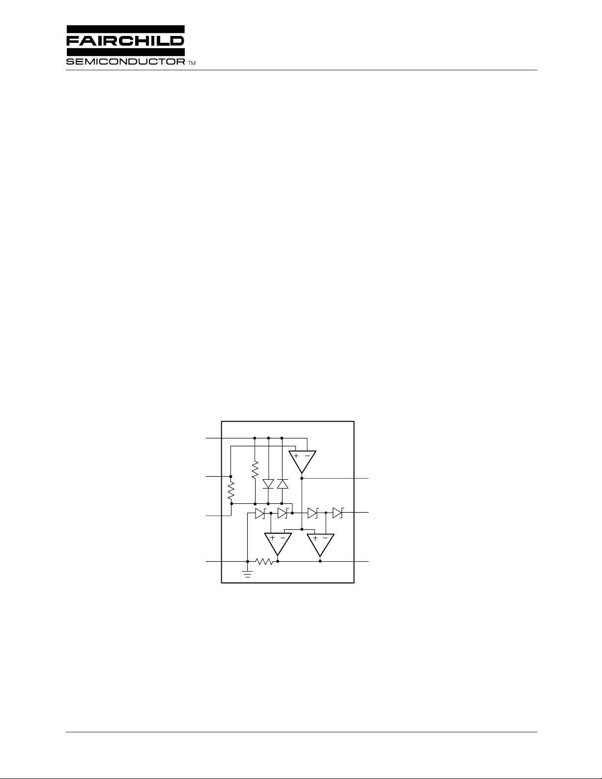
Block Diagram
V
FB
+Input
V
REF
(+13V)
Ground
RV4145A
R1
10K
R2
10K
6.5V
4.7K
R3
6.5V
6.5V
6.5V
65-4145A-01
Op Amp Output
+V
S
(+26V)
SCR Trigger
REV. 1.0.3 3/6/02
Page 2
PRODUCT SPECIFICATION RV4145A
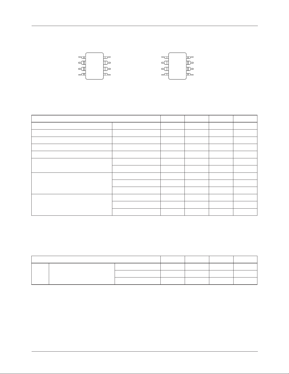
Pin Assignments
8-Pin PDIP
V
FB
+Input
V
REF
GND
8-Pin SOIC
8
1
7
2
6
3
5
4
NC
Op Amp Output
+V
S
SCR Trigger
+Input
V
GND
NC
REF
8-Pin MSOP
8
1
7
2
6
3
5
4
V
FB
Op Amp Output
+V
S
SCR Trigger
65-4145A-02
Absolute Maximum Ratings
(beyond which the device may be damaged)
Parameter Min Typ Max Units
Supply Current 18 mA
Internal Power Dissipation 500 mW
Storage Temperature Range -65 +150 °C
Operating Temperature Range -35 +85 °C
Junction Temperature 125°C
Lead Soldering Temperature 60 Sec, DIP 300 °C
T
< 50°C SOIC 300 mW
P
D
A
For T
> 50°C Derate at SOIC 4 mW/°C
A
Notes:
1. Functional operation under any of these conditions is NOT implied. Performance and reliability are guaranteed only if
Operating Conditions are not exceeded.
1
10 Sec, SOIC, MSOP 260 °C
PDIP 450 mW
MSOP 350 mW
PDIP 6 mW/°C
MSOP 4.7 mW/°C
Operating Conditions
Parameter Min Typ Max Units
θ
JA
2
Thermal resistance SOIC 240 °C/W
PDIP 160 °C/W
MSOP 206 °C/W
REV. 1.0.3 3/6/02
Page 3
≤
RV4145A PRODUCT SPECIFICATION
Electrical Characteristics
Parameters Test Conditions Min Typ Max Units
Detector Reference Voltage Pin 7 to Pin 3 6.8 7.2 8.1 ±V
Shunt Regulator
Zener Voltage (+V
Reference Voltage (V
Quiescent Current (I
Operational Amplifier
Offset Voltage Pin 2 to Pin 3 -3.0 0.5 +3.0 mV
+Output Voltage Swing Pin 7 to Pin 3 6.8 7.2 8.1 V
–Output Voltage Swing Pin 7 to Pin 3 -9.5 -11.2 -13.5 V
+Output Source Current Pin 7 to Pin 3 650 µA
–Output Source Current Pin 7 to Pin 3 1.0 mA
Gain Bandwidth Product F = 50KHz 1.0 1.8 MHz
Resistors I
R1 Pin 1 to Pin 3 10 k Ω
R2 Pin 2 to Pin 3 10 k Ω
R3 Pin 5 to Pin 4 3.5 4.7 5.9 k Ω
SCR Trigger Voltage Pin 5 to Pin 4
Detector On 1.5 2.8 V
Detector Off 0 1 10 mV
) Pin 6 to Pin 4 25 26 29.2 V
S
) Pin 3 to Pin 4 12.5 13 14.6 V
REF
)+V
S
(I
= 1.5mA and T
S
= 24V 450 750 µA
S
= 0mA
S
= +25°C)
A
Electrical Characteristics
Parameters Test Conditions Min Typ Max Units
Detector Reference Voltage Pin 7 to Pin 3 6.5 7.2 8.3 ±V
Shunt Regulator
Zener Voltage (+V
Reference Voltage (V
Quiescent Current (I
Operational Amplifier
Offset Voltage Pin 2 to Pin 3 -5.0 0.5 +5.0 mV
+Output Voltage Swing Pin 7 to Pin 3 6.5 7.2 8.3 V
–Output Voltage Swing Pin 7 to Pin 3 -9 -11.2 -14 V
Gain Bandwidth Product F = 50KHz 1.8 MHz
Resistors I
R1 Pin 1 to Pin 3 10 k Ω
R2 Pin 2 to Pin 3 10 k Ω
R3 Pin 5 to Pin 4 3.5 4.7 5.9 k Ω
SCR Trigger Voltage Pin 5 to Pin 4
Detector On 1.3 2.8 V
Detector Off 0 3 50 mV
) Pin 6 to Pin 4 24 26 30 V
S
) Pin 3 to Pin 4 12 13 15 V
REF
)+V
S
(I
= 1.5mA and -35°C ≤ T
S
= 23V 500 µA
S
= 0mA
S
A
+85°C)
REV. 1.0.3 3/6/02
3
Page 4

×
PRODUCT SPECIFICATION RV4145A
Principles of Operation
The 26V shunt regulator voltage generated by the string of
zener diodes is divided into three reference voltages: 3/4 V
1/2 V
, and 1/4 V
S
ence to create an artifical ground of +13V at the op amp noninverting input.
Figure 1 shows a three-wire 120V AC outlet GFI application
using an RV4145A. Fault signals from the sense transformer
are AC coupled into the input and are amplified according to
the following equation:
V
= R
7
Where V
R
SENSE
pin 7 to pin 1, I
N is the turns ratio of the transformer. When V
or minus 7.2V relative to pin 3 the SCR Trigger output will
go high and fire the external SCR.
The formula for V
include the sense transformer characteristics.
Grounded neutral fault detection is accomplished when a
short or fault closes a magnetic path between the sense transformer and the grounded neutral transformer. The resultant
AC coupling closes a positive feedback path around the op
amp, and therefore the op amp oscillates. When the peaks of
the oscillation voltage exceed the SCR trigger comparator
thresholds, the SCR output will go high.
is the RMS voltage at pin 7 relative to pin 3,
7
is the value of the feedback resistor connected from
Shunt Regulator
R
limits the current into the shunt regulator; 220V
LINE
applications will require substituting a 47k Ω 2W resistor. In
addition to supplying power to the IC, the shunt regulator
creates internal reference voltages (see above).
Operational Amplifier
R
sensitivity to normal faults. To adjust R
procedure: apply the desired fault current (a difference in
current of 5mA is the UL 943 standard). Adjust R
upward until the SCR activates. A fixed resistor can be used
for R
will meet UL’s 943 4-6mA specification window.
is a feedback resistor that sets gain and therefore
SENSE
SENSE
. V
S
SENSE
SENSE
, since the resultant ±15% variation in sensitivity
is at 1/2VS and is used as a refer-
REF
I
is approximate because it does not
7
/N
SENSE
is the fault current in amps RMS and
exceeds plus
7
, follow this
SENSE
SENSE
The roll-off frequency is greater than the grounded neutral
fault oscillation frequency, in order to preserve loop gain for
oscillation (which is determined by the inductance of the
,
S
200:1 transformer and C4).
The senstivity to grounded neutral faults is adjusted by
changing the frequency of oscillation. Increasing the frequency reduces the sensitivity by reducing the loop gain of
the positive feedback circuit. As frequency increases, the
signal becomes attenuated and the loop gain decreases. With
the values shown the circuit will detect a grounded neutral
fault having resistance of 2 Ω or less.
The input to the op amp are protected from overvoltage by
back-toback diodes.
SCR Driver
The SCR used must have a high dV/dt rating to ensure that
line noise (generated by noisy appliances such as a drill
motor) does not falsely trigger the SCR. Also, the SCR must
have a gate drive requirement of less than 200µA. C
noise filter capacitor that prevents narrow pulses from firing
the SCR.
The relay solenoid used should have a 3ms or less response
time in order to meet the UL 943 timing requirement.
is a
F
Sense Transformers and Cores
The sense and grounded neutral transformer cores are usually fabricated using high permeability laminated steel rings.
Their single turn primary is created by passing the line and
neutral wires through the center of its core. The secondary is
usually from 200 to 1500 turns.
Magnetic Metals Corporation, Camden, NJ 08101,
(609) 964-7842, and Magnetics, 900 E. Butler Road,
P.O. Box 391, Butler, PA 16003, (412) 282-8282 are full line
suppliers of ring cores and transformers designed specifically for GFI applications.
Two-Wire Application Circuit
Figure 2 shows the diagram of a 2-wire 120V AC outlet GFI
circuit using an RV4145A. This circuit is not designed to
detect grounded neutral faults. Thus, the grounded neutral
transformer and capacitors C3 and C4 of Figure 1 are not
used.
4
REV. 1.0.3 3/6/02
Page 5

RV4145A PRODUCT SPECIFICATION
Press
R
TEST
To Test
Line
Mov
Sense Transformer
1000:1
C1
10µF
15K
Hot
Neutral
V
V
GND
FB
REF
R
SENSE
1M *
RV4145
Op Amp Output
(+13V)
+V
SCR Trigger
Ground Neutral
Transformer
200:1
C3
0.01 µF
C4
S
R
LINE
24K
C
F
2.2 µF
0.03 µF
Q1 ON Semi
MCR100-6
C2
0.01µF
Latching
Contacts
K1
Load
Solenoid
DB1
1N4004 (4)
* Value depends on transformer characteristics.
Figure 1. GFI Application Circuit (Three-Wire Outlet)
65-4145A-03
REV. 1.0.3 3/6/02
5
Page 6

PRODUCT SPECIFICATION RV4145A
Press
R
SENSE
1M *
To Test
Latching
Contacts
K1
Load
Line
Mov
Sense Transformer
1000:1
R
TEST
15K
Hot
Neutral
C1
10µF
V
V
GND
FB
REF
RV4145
Op Amp Output
(+13V)
SCR Trigger
+V
Solenoid
S
R
LINE
24K
Q1 Tag
X0103DA
DB1
1N4004 (4)
C2
0.01µF
65-4145A-04
* Value depends on transformer characteristics.
Figure 2. GFI Application Circuit (Two-Wire Outlet)
C
F
2.2 µF
6
REV. 1.0.3 3/6/02
Page 7

RV4145A PRODUCT SPECIFICATION
Schematic Diagram
(6)
S
+V (+26V)
Q20
6.5V
R7
250K
Q13
Q11
Q19
Q12
6.5V
(3)
Q15
Q23
REF
V
(+13V)
Q18
R14
6.5V
1.3K
R13
30K
R6
Q17
450
6.5V
Q16
Q14
R12
Z1
7.2K
5.6V
Q10
R9
Q9
R3
39K
4.7K
(4)
Ground
Substrate
(5)
(7)
65-4145A-05
SCR Trigger
Op Amp Output
R2
R10
6K
10K
R1
10K
Q3
Q22
Q21
(1)
(+)
(-)
Q1
Q2
C1
4 pF
Q8
Q7
R5
50K
Q5
R4
Q6
C2
FB
(2)
V
+Input
50K
Q4
10 pF
REV. 1.0.3 3/6/02
7
Page 8

PRODUCT SPECIFICATION RV4145A
Mechanical Dimensions
8-Lead Plastic DIP Package
Symbol
A — .210 — 5.33
A1 .015 — .38 —
A2 .115 .195 2.93 4.95
B .014 .36
B1 .045 .070 1.14 1.78
C .008 .015 .20 .38
D .348 .430 8.84 10.92
D1
E
E1
e
eB
L
N
E1
Inches
Min. Max. Min. Max.
.022 .56
.005 — .13 —
.300 .325 7.62 8.26
.240 .280 6.10 7.11
.100 BSC 2.54 BSC
— .430 — 10.92
.115 .160 2.92 4.06
8° 8° 5
D
4
1
Millimeters
Notes
4
2
2
Notes:
1.
Dimensioning and tolerancing per ANSI Y14.5M-1982.
2.
"D" and "E1" do not include mold flashing. Mold flash or protrusions
shall not exceed .010 inch (0.25mm).
3.
Terminal numbers are for reference only.
4.
"C" dimension does not include solder finish thickness.
5.
Symbol "N" is the maximum number of terminals.
5
D1
A
A1
B1
8
e
A2
L
B
E
C
eB
8
REV. 1.0.3 3/6/02
Page 9

RV4145A PRODUCT SPECIFICATION
Mechanical Dimensions
(continued)
8-Lead SOIC Package
Symbol
A .053 .069 1.35 1.75
A1 .004 .010 0.10 0.25
B .013 0.33
C .008 .010 0.20 0.25
D .189 .197 4.80 5.00
E .150 .158 3.81 4.01
e
H
h
L .016 .050 0.40 1.27
N8 8
α
ccc .004 0.10——
85
Inches
Min. Max. Min. Max.
.020 0.51
.050 BSC 1.27 BSC
.228 .244 5.79 6.20
.010 .020 0.25 0.50
0° 8° 0° 8°
EH
Millimeters
Notes
5
2
2
3
6
Notes:
1.
Dimensioning and tolerancing per ANSI Y14.5M-1982.
2.
"D" and "E" do not include mold flash. Mold flash or
protrusions shall not exceed .010 inch (0.25mm).
3.
"L" is the length of terminal for soldering to a substrate.
4.
Terminal numbers are shown for reference only.
5.
"C" dimension does not include solder finish thickness.
6.
Symbol "N" is the maximum number of terminals.
14
D
A
e
B
A1
SEATING
PLANE
– C –
LEAD COPLANARITY
ccc C
h x 45°
C
α
L
REV. 1.0.3 3/6/02
9
Page 10

PRODUCT SPECIFICATION RV4145A
Mechanical Dimensions
8-Lead MSOP Package
Package MA08D
0.118 - 0.004
[3 ± 0.1]
–A–
85
SYMM
C
0.193 ± 0.004
[4.9 ± 0.1]
PIN 1
IDENT
14
0.030 - 0.037
[0.78 - 0.94]
–C–
0.002 [0.05]
0.002 - 0.006
[0.06 - 0.15]
TYP
C
0.012 ± 0.002
[0.3 ± 0.05]
0.002 [0.05]
TYP
MSA
0.118 ± 0.004
(0.0256)
[0.65]
(0.033)
[0.84]
SB
[3 ± 0.1]
–B–
TYP
(0.040)
TYP
[1.02]
(0.016)
TYP
[0.41]
LAND PATTERN RECOMMENDATION
0.005
TYP
R
[0.13]
0.005
TYP
R
[0.13]
0.021 ± 0.005
0.0375
[0.953]
0.007 ± 0.002
[0.18 ± 0.05]
[0.53 ± 0.12]
TYP
(0.189)
[4.8]
(0.0256)
TYP
[0.65]
0°–6° TYP
SEATING PLANE
GAGE
PLANE
(0.010)
[0.23]
8-Lead Molded Small Outline Package (MSOP), JEDEC MO-187, 3.0mm Wide
Package Number MA08
D
10 REV. 1.0.3 3/6/02
Page 11

PRODUCT SPECIFICATION RV4145A
Ordering Information
Part Number Package Operating Temperature Range
RV4145AN 8-Lead Plastic DIP -35°C to +85°C
RV4145AM 8-Lead Plastic SOIC -35°C to +85°C
RV4145AMU 8-Lead Plastic MSOP -35°C to +85°C
DISCLAIMER
FAIRCHILD SEMICONDUCTOR RESERVES THE RIGHT TO MAKE CHANGES WITHOUT FURTHER NOTICE TO ANY
PRODUCTS HEREIN TO IMPROVE RELIABILITY, FUNCTION OR DESIGN. FAIRCHILD DOES NOT ASSUME ANY
LIABILITY ARISING OUT OF THE APPLICATION OR USE OF ANY PRODUCT OR CIRCUIT DESCRIBED HEREIN; NEITHER
DOES IT CONVEY ANY LICENSE UNDER ITS PATENT RIGHTS, NOR THE RIGHTS OF OTHERS.
LIFE SUPPORT POLICY
FAIRCHILD’S PRODUCTS ARE NOT AUTHORIZED FOR USE AS CRITICAL COMPONENTS IN LIFE SUPPORT DEVICES
OR SYSTEMS WITHOUT THE EXPRESS WRITTEN APPROVAL OF THE PRESIDENT OF FAIRCHILD SEMICONDUCTOR
CORPORATION. As used herein:
1. Life support devices or systems are devices or systems
which, (a) are intended for surgical implant into the body,
or (b) support or sustain life, and (c) whose failure to
perform when properly used in accordance with
instructions for use provided in the labeling, can be
reasonably expected to result in a significant injury of the
user.
2. A critical component in any component of a life support
device or system whose failure to perform can be
reasonably expected to cause the failure of the life support
device or system, or to affect its safety or effectiveness.
www.fairchildsemi.com
3/6/02 0.0m 001
2002 Fairchild Semiconductor Corporation
Stock#DS2004145A
 Loading...