

Page 1
RV4140A
Low Power Two-Wire Ground Fault
Interrupter Controller
www.fairchildsemi.com
Features
• Powered from the AC line
• Built-in bridge rectifier
• Direct interface to SCR
• 350 mA quiescent current
• Adjustable trip current
• Adjustable time delay
• Minimum external components
• Meets UL 943 requirements
• Specifically for two-wire systems
• For use with 110V or 220V systems
Description
The RV4140A is a low power controller for AC outlet
appliance leakage circuit interrupters. These devices detect
hazardous current paths to ground such as an appliance
falling into water. The interrupter then open circuits the line
before a harmful or lethal shock occurs.
Internally, the RV4140A has a diode bridge rectifier, zener
shunt regulator, op amp, current reference, time delay circuit,
latch and SCR driver.
An external sense transformer, SCR, relay, two resistors
and three capacitors complete the design of the circuit
interrupter. The simple layout and minimum component
count ensure ease of application and long term reliability.
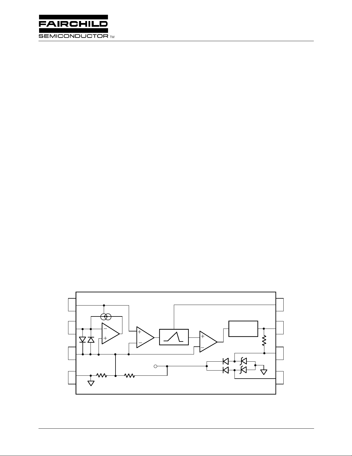
Block Diagram
1
2
3
4
RV4140A
8
Latch
4.7K
Delay
V
cc
7
6
5
65-4140A-01
Rev. 1.0.0
Page 2

RV4140A PRODUCT SPECIFICATION
Functional Description
(Refer to Block Diagram and Figure 1 )
The shunt regulator generated by a 6.5V zener diode is
built into the internal bridge rectifier. It is divided to create
an internal reference voltage of 2.9V connected to pin 3.
The secondary of the sense transformer is AC coupled to the
inverting input of the sense amplifier at pin 2; the non-inverting input is referenced to pin 3. A current feedback loop
around the sense amplifier ensures a virtual ground will be
presented to the secondary of the sense transformer. In this
manner it acts as a current transformer instead of a voltage
transformer. In this mode, the transformer’s characteristics
are very predictable and circuit adjustments are not necessary in production.
The sense transformer has a toroidal core made of laminated
steel rings or solid ferrite material. The secondary of the
transformer is 500 to 1000 turns of #40 wire wound through
the toroid. The primary’s one turn made by passing the
AC hot and neutral wires through the center of the toroid.
When a ground fault exists, a difference exists between the
current flowing in hot and neutral wires. The difference
primary current, divided by the number of secondary turns,
flows through the secondary wire of the transformer.
The AC coupled transformer secondary current then flows
through the sense amplifier’s feedback loop, creating a full
wave rectified version of the secondary fault current. This
current passes through R
equal to R
sense transformer turns ratio. This voltage is compared with
the reference voltage at pin 3.
If the voltage at pin 1 is greater than pin 3, a comparator will
charge C2 through a 29 mA current source at pin 8. If the
voltage at pin 1 exceeds pin 3 for longer than the delay time,
a 400 mA current will pulse between pins 7 and 6 which will
trigger the gate of the SCR.
If the voltage at pin 1 exceeds pin 3 for less than the delay
time, the SCR will not trigger.
The fault current at which the controller triggers the SCR
is dependent on the value of R
determined by C2.
times the peak fault current divided by the
SET
at pin 1, generating a voltage
SET
and the time delay
SET
Supply Current Requirements
The RV4140A has a built-in diode bridge rectifier that
provides power to the chip independent of the polarity of
the A C line. This eliminates the external rectifier required for
previous GFCI controllers.
R
limits the shunt regulator current to 2 mA. The rec-
LlNE
ommended value is 47K to 91K for 110V systems and 91K
to 150K for 220V systems. The recommended maximum
peak line current through R
DO NOT connect a filter capacitor between pins 5 and 6 in
an attempt to filter the supply voltage at the RV4140A.
Proper operaton of the R V4140A requires the internal supply
voltage to be unfiltered.
LlNE
is 7 mA.
SCR Driver
The SCR must have a high dV/dt rating to ensure that line
noise (generated by electrically noisy appliances) does not
falsely trigger the SCR. Also, the SCR must ha ve a gate dri ve
requirement less than 200 mA. C3 is a noise filter that
prevents high frequency line pulses from triggering the SCR.
The relay solenoid used should have a 3 ms or less response
time to meet the UL 943 timing requirement.
Supplier of Sense Transformers and Cores
Magnetic Metals Corporation, Camden, NJ 08101,
(609) 964-7842, supplies a full line of ring cores and transformers designed specifically for GFCI and related applications.
Determining the Values of RSET and C2
Determine the ground fault trip current requirement. This
will be typically 5 mA in North America (117 VAC) and
10 mA in the UK and Europe.
Determine the minimum amount of time delay required to
prevent nuisance tripping. This will typically be 1 to 2 ms.
The value of C2 required to provide the desired delay time
is:
C2 = 10 x T
where C2 is in nF, and T is the desired delay time in ms.
UL 943 requires the circuit interrupter trip when the ground
fault exceeds 6 mA and not trip when the fault current is less
than 4 mA.
2
Page 3
PRODUCT SPECIFICATION RV4140A
The value of R
to meet nominal ground fault tip current
SET
specification is:
R
SET
---------------------------------------------------------------=
I
FAULT
2.05 N´
COS 180´ TP¤()
Where:
•R
SET
is in kW
• T is the time delay in ms
• P is the period of the line frequency in ms
•I
is the desired ground fault trip current in mA
FAULT
RMS.
• N is the number of sense transformer secondary turns.
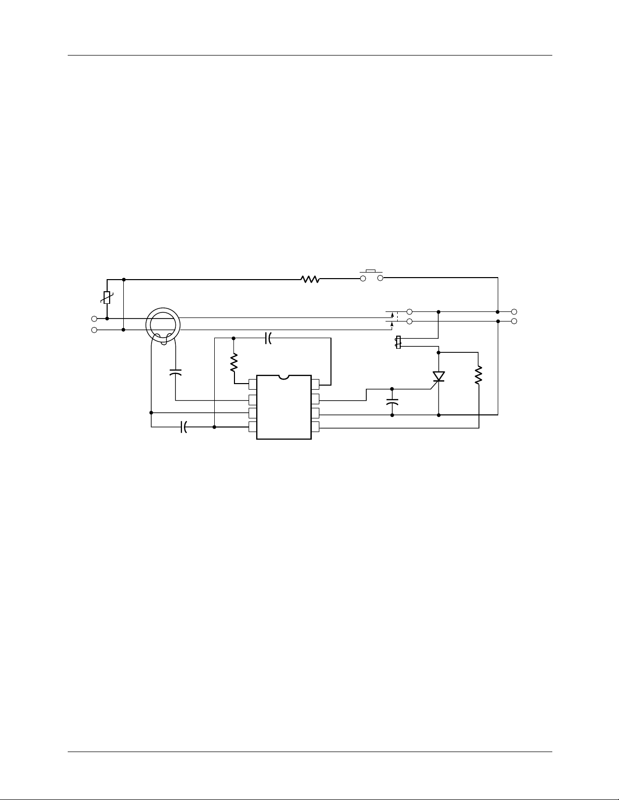
Sense Transformer
Mov
Line
1:500 Turns Ratio
3 Ring Steel Core
10 F
C1
m
C4
m
0.1 F
Hot
Neutral
R
SET
191K
1
2
3
4
C2
0.02 F
RV4140A
This formula assumes an ideal sense transformer is used.
The calculated value of R
may have to be changed up to
SET
30% when using a non-ideal transformer.
R
TEST
15K
m
8
7
6
5
Press to Test
Normally
Latching
Solinoid
Closed
Contacts
Q1
Tag
X0103DA
C3
10 nF
R
LINE
91K
Load
65-4140A-02
Figure 1. Appliance Leakage Detector Circuit Application
3
Page 4
RV4140A PRODUCT SPECIFICATION
Pin Assignments
PDIP
(Top View)
SOIC
(Top View)
1
R
SET
VFB
2
2.9V
3
Ground 5
4
8
C Delay
7
SCR Trigger
6
Neutral
Line
R
1
SET
2
VFB
3
2.9V
Ground 5
4
65-4140A-03
8
C Delay
7
SCR Trigger
6
Neutral
Line
Absolute Maximum Ratings
Parameter Min. Typ. Max. Units
Supply Current 7mA
Internal Power Dissipation 500 mW
Storage Temperature Range -65 +150 °C
Operating Temperature Range -35 +80 °C
Lead Soldering Temperature 60 Seconds, DIP +300 °C
10 Seconds, SOIC +260 °C
Thermal Characteristics
Parameter 8 Lead Plastic SOIC 8 Lead Plastic DIP
Maximum Junction Temperature +125°C +125°C
Maximum P
Thermal Resistance, q
For TA > 50°C Derate at 4.1 mW/°C 6.25 mW/°C
<50°C 300 mW 468 mW
DTA
JA
240°C/W 160°C/W
4
Page 5

PRODUCT SPECIFICATION RV4140A
Electrical Characteristics
I
= 1.2mA and TA = +25°C, R
LINE
Parameters Test Conditions Min. Typ. Max. Units
Shunt Regulator (Pins 5 to 4)
Regulated Voltage I
Regulated Voltage I
Sense Amplifier (Pins 2 to 3)
Offset Voltage Design Value -3.0 0 3.0 mV
Gain Bandwidth Design Value 2.0 MHz
Input Bias Current Design Value 30 100 nA
SCR Trigger (Pins 7 to 6)
Output Resistance V
Output Voltage I
Output Voltage I
Output Current V
Reference Voltage (Pins 3 to 4)
Reference Voltage I
Delay Timer (Pins 8 to 4)
Delay Time
1
Delay Current I
Note:
1. Delay time is defined as starting when the instantaneous sense current (I
trigger voltage V
goes high.
7-6
SET
= 290kW
C
= 11mA 6.8 7.2 7.6 V
2-3
= 700 mA, I
LINE
= open, I
5-6
= 9mA 0 0.1 10 mV
2-3
= 11mA 1.4 2.0 2.6 V
2-3
= 0V, I
7-6
LINE
8-4
= 11mA 232935mA
2-3
2-3
= 700 mA 2.6 2.9 3.2 V
= 20nF — 2.0 — ms
= 9mA 6.8 7.2 7.6 V
2-3
= 0mA 4.0 4.7 5.4 kW
2-3
= 11mA 300 420 600 mA
) exceeds 2.9V/R
2-3
and ending when the SCR
SET
5
Page 6

RV4140A PRODUCT SPECIFICATION
Schematic Diagram
(6)
Neutral
Q38
Q25
R10
Q32
Q24
SCR
Q26
4.7K
Q39
(7)
(8)
Cap
Q50
Q49
Q41
R9
83K
Sub
Sub
Q42
Q40
Q31
Q30
Q29
Q28
65-4653
Sub
(5)
Line
Q48
Q47
Q46
Q45
Q44
Q43
Q37
Q36
Q34
Q33
Q27
Q35
Sub
Q22
Q15
Q14Q12
Q13
Q23
Q21
Q18
R7
23K
Q16
R3
8.5K
Q5
V
Q3
FB
Q44
Q17
C1
R2
10K
CC
V
R1
10K
Q2
(2)
(3)
Common
Q19
6.5 pF
Q20
Q9
Q7
Q11
R8
23K
(1)
SET
2.5K
50K
(4)
Ground
R
Q8
Q6
Q10
R6
R5
50K
R4
6
Page 7

PRODUCT SPECIFICATION RV4140A
Notes:
7
Page 8

RV4140A PRODUCT SPECIFICATION
Notes:
8
Page 9

PRODUCT SPECIFICATION RV4140A
Notes:
9
Page 10

RV4140A PRODUCT SPECIFICATION
Mechanical Dimensions
8-Lead Plastic DIP Package
Symbol
A — .210 — 5.33
A1 .015 — .38 —
A2 .115 .195 2.93 4.95
B .014 .36
B1 .045 .070 1.14 1.78
C .008 .015 .20 .38
D .348 .430 8.84 10.92
D1
E
E1
e
eB
L
N
E1
Inches
Min. Max. Min. Max.
.022 .56
.005 — .13 —
.300 .325 7.62 8.26
.240 .280 6.10 7.11
.100 BSC 2.54 BSC
— .430 — 10.92
.115 .160 2.92 4.06
8¡ 8¡ 5
D
4
1
Millimeters
Notes
4
2
2
Notes:
1.
Dimensioning and tolerancing per ANSI Y14.5M-1982.
2.
"D" and "E1" do not include mold flashing. Mold flash or protrusions
shall not exceed .010 inch (0.25mm).
3.
Terminal numbers are for reference only.
4.
"C" dimension does not include solder finish thickness.
5.
Symbol "N" is the maximum number of terminals.
5
D1
A
A1
B1
8
e
A2
L
B
E
C
eB
10
Page 11

PRODUCT SPECIFICATION RV4140A
Mechanical Dimensions (continued)
8-Lead SOIC Package
Symbol
A .053 .069 1.35 1.75
A1 .004 .010 0.10 0.25
B .013 0.33
C .008 .010 0.20 0.25
D .189 .197 4.80 5.00
E .150 .158 3.81 4.01
e
H
h
L .016 .050 0.40 1.27
N8 8
a
ccc .004 0.10——
85
14
Inches
Min. Max. Min. Max.
.020 0.51
.050 BSC 1.27 BSC
.228 .244 5.79 6.20
.010 .020 0.25 0.50
0¡ 8¡ 0¡ 8¡
EH
Millimeters
Notes
Notes:
1.
Dimensioning and tolerancing per ANSI Y14.5M-1982.
2.
"D" and "E" do not include mold flash. Mold flash or
protrusions shall not exceed .010 inch (0.25mm).
3.
"L" is the length of terminal for soldering to a substrate.
4.
5
2
2
3
6
Terminal numbers are shown for reference only.
5.
"C" dimension does not include solder finish thickness.
6.
Symbol "N" is the maximum number of terminals.
D
A
e
B
A1
SEATING
PLANE
– C –
LEAD COPLANARITY
ccc C
a
h x 45¡
C
L
11
Page 12

RV4140A PRODUCT SPECIFICATION
Ordering Information
Part Number Package Operating Temperature Range
RV4140AN 8-Lead Plastic DIP -35°C to +80°C
RV4140AM 8-Lead Plastic SOIC -35°C to +80°C
LIFE SUPPORT POLICY
FAIRCHILD’S PRODUCTS ARE NOT AUTHORIZED FOR USE AS CRITICAL COMPONENTS IN LIFE SUPPORT DEVICES
OR SYSTEMS WITHOUT THE EXPRESS WRITTEN APPROVAL OF THE PRESIDENT OF FAIRCHILD SEMICONDUCTOR
CORPORATION. As used herein:
1. Life support devices or systems are devices or systems
which, (a) are intended for surgical implant into the body,
or (b) support or sustain life, and (c) whose failure to
perform when properly used in accordance with
instructions for use provided in the labeling, can be
reasonably expected to result in a significant injury of the
user.
2. A critical component in any component of a life support
device or system whose failure to perform can be
reasonably expected to cause the failure of the life support
device or system, or to affect its safety or effectiveness.
www.fairchildsemi.com
7/27/98 0.0m 002
Ó 1998 Fairchild Semiconductor Corporation
Stock#DS20004140A
 Loading...