

Page 1

RTL8181 Wireless LAN Access Point/Gateway Controller
DATA SHEET
ISSUE 4: June 10, 2003
Page 2

Issue
and function
Victor/David
Revision History
RTL8181
Revision
Issue 1
0.1
Issue 2 0.2
Issue 3 0.3
Issue 4 1.0
Details of Change Originator Issue Date
First Release David Hsu 11/29/2002
1. Add a section about system configuration.
2. Add some descriptions about register usages.
1. Add Pin number
2. Add System config register
David Hsu 12/9/2002
Victor Hsu 03/03/2003
1. Add a memory map.
2. Modify some register definitions
descriptions.
3. Add package information.
2003/06/10
4. Remove 32 bits flash interface support
5. Add pin definitions for Maxim RF interface
CONFIDENTIAL v1.0
2
Page 3

RTL8181
Table of Contents
1. OVERVIEW................................................................................................................................... 4
2. PIN DESCRIPTION................................................................................................................. 5
3. ADDRESS MAPPING...........................................................................................................12
4. REGISTER MAPPING......................................................................................................... 13
5. SYSTEM CONFIGURATION.......................................................................................... 16
6. INTERRUPT CONTROLLER........................................................................................17
7. MEMORY CONTROLLER............................................................................................... 18
8. ETHERNET CONTROLLER.......................................................................................... 21
9. UART CONTROLLER......................................................................................................... 30
10. TIMER & WATCHDOG...................................................................................................33
11. GPIO CONTROL...................................................................................................................35
12. 802.11B WLAN CONTROLLER.................................................................................37
13. PACKAGE INFORMATION ......................................................................................... 48
CONFIDENTIAL v1.0
3
Page 4
RTL8181
EJTAG
1. Overview
RTL8181 is a highly integrated SoC, embedded with a high-performance 32-bit RISC microcontroller, Ethernet and WLAN
controller. It is a cost-effective and high-performance solution for the system of wireless LAN Access Point, wireless SOHO
router, wireless Internet gateway, etc.
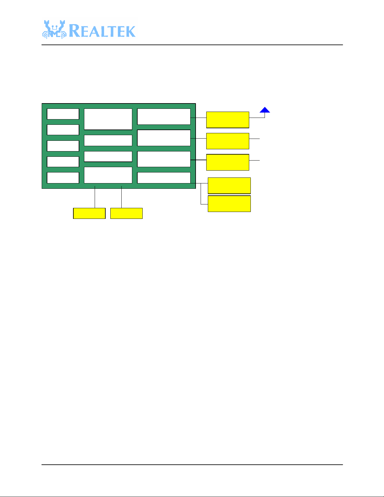
System block diagram:
Timer
Watchdog
UART
GPIO
The embedded processor of RTL8181 is Lexra LX5280 32bit RISC CPU, with 8K separate instruction and data caches. A
protection unit (MMU) allows the memory be segmented and protected, and this unit is required in the modern operation
system (e.g., Linux).
The processor pipeline is a dual-issues and 6 stage architecture. The dual- issue CPU fetches two instructions per cycle, and
which could allow two instructions are executed concurrently in two pipes via some instructions. Thus, its performance will
achieve up to 30% improvement over uni-scalar architecture.
Besides, it includes two fast Ethernet MACs, one could be used for LAN interface and the other one could connect to WAN
port. An IEEE 802.11b WLAN MAC+Baseband processor is embedded as well. By this build-in wireless controller, it could
save a lot of costs and space comparing with the system designed with an external 802.11b adapter.
The RTL8181 also integrates with memory controller, which allows customers use external SDRAM and Flash memory in
glueless.
A PCI interface is supported as well, which enables customers to plug in a PCI device seamlessly. For example, an IEEE
802.11a device could be connected through this PCI interface to provide the WLAN dual mode service.
Features
Core Processor
? LX5280 32-bit RISC architecture.
? Superscalar architecture, containing 2 execution pipelines with better performance
? Embedded with 8K I-Cache, 8K D-Cache and 4K D-RAM.
? MMU supported
? Up to 200MHZ operating frequency
WLAN Controller
? Integrated IEEE 802.11b complied MAC and DSSS Baseband processor
? Support Tx data rate in 11M, 5.5M, 2M and 1M
? Support long and short preamble
? Support antenna diversity and AGC.
? Embedded with encryption/decryption engine for 64 bits and 1 28 bits WEP
CONFIDENTIAL v1.0
Microprocessor 802.11b MAC/BB
Cache buffer
MMU
Memory controller
Flash SDRAM
Ethernet MAC0
Ethernet MAC1
PCI Bridge
RF transceiver
MII
Ethernet PHY
MII
Ethernet PHY
PCI device
PCI device
4
LAN
WAN
Page 5
RTL8181
Fast Ethernet Controller
? Fully compliant with IEEE 802.3/802.3u
? Support MII interface with full and half duplex capability
? Support descriptor-based buffer management with scatter-gather capability
? Support IP, TCP and UDP checksum offload
? Support IEEE 802.1Q VLAN tagging and 802.1P priority queue.
? Support full duplex flow control (IEEE 802.3X)
UART
? 16550 compatible
? 16 bytes FIFO size
? Auto CTS/RTS flow control
Memory Controller
? Support external 16/32-bit SDRAM with 2 banks access, up to 32M bytes
? Support external 16-bit Flash memory, up to 16M bytes
PCI Bridge
? Support two external PCI devices, complied with PCI 2.2
? Support PCI master/slave mode
? 3.3 and 5V I/O tolerance
GPIO
? 16 programmable I/O ports and more 16 port when memory interface is 16 bit mode.
? Individually configurable to input, output and edge transition
Watchdog/Timer/Counter
? A hardware watchdog timer, used to reset processor when system hangs up
? 4 sets of general timers/counters
EJTAG
? Standard P1149.1 JTAG interface for testing and debugging
2. Pin Description
Symbol Type Pin No(208) Pin No(292) Description
Memory Interface
MD[31-0] I/O 198,197,195
,194,193,19
2,191,190,1
88,187,185,
184,182,181
,180,179,17
7,176,174,1
73,171,170,
169,168,166
,165,163,16
2,161,160,1
59,158
MA[21-0]/
DQM[3-0]
CONFIDENTIAL v1.0
O 115,116,118
,119,121,12
2,124,125,1
27,128,130,
131,133,134
,135,136,13
P1,P2,N3,N
2,N1,M3,M
2,M1,L2,L3,
L1,K2,K3,K
1,J2,J1,H2,
H1,G2,F1,G
3,F2,E1,F3,
E2,D1,D2,E
3,A1,B1,B2,
C3
B14,A15,D1
4,C14,A14,
C13,B13,C1
2,A12,C11,
B11,C10,A1
1,B10,A10,
Data for SDRAM, Flash.
Address for SDRAM, Flash.
MA[15-18] mapping to DQM[3-0] for SDRAM
5
Page 6

RTL8181
8,139,141,1
42,144
M_CLK O 152 A5 SDRAM clock
MCS0B O 150 C5 Bank 0 chip select FLASH chip select
MCS1B O 149 B5, Bank 1 chip select FLASH chip select
RASB/OEB O 157 D4 Raw address strobe for SDRAM;
CASB O 156 A2 Column address strobe
MWENB O 154 B4 Write enable for SDRAM and Flash
MCKE O 153 A4 SDRAM Clock enable
MCS2B O 147 D5 Bank 0 chip select for SDRAM
MCS3B O 146 B6 Bank 1 chip select for SDRAM
UART Interface
URTSB O 16 Y8 UART Request to send
UCTSB
USIN I 15
USOUT O 17
Power & GND
PP[11-1] P 208,178,164
GP[11-1] P 204,189,167
PD[7:5],PS
[5:3]
GD[7-5],G
S[5-3]
PA[6-1] P 111,104,92,1
GA[6-1],G
A7
PD[4-1] P 120,72,48,28 J4,H4,D10,
GD[4-1] P 117,69,45,25 H13,H12,H
PS[2:1] P 36,7 D6,C6,U4,U
GS[2:1] P 39,10 D8,D7,T4,U
WLAN Traffic LED Control
WLTXRX
LED0B
CONFIDENTIAL v1.0
I 14
,151,137,12
3,83,58,52,3
0,4
,155,140,12
6,80,63,42,2
0,1
P 183,175,132
,196,148,74
P 186,172,129
,199,145,77
13,98,89
P 108,107,95,
114,100,86,
112
O 65 T19 WLAN Tx/Rx traffic indicator or JTAG reset.
C9,A9,B9,A
7,C7,B7,A6
Output enable for Flash
W7 UART Clear to send.
Y7 UART data receive serial input
V8 UART data transmit serial output
K4,G4,F4,E
4,D13,D12,
D11,B18,B1
7,A19,A18,
K17,P4,P17,
R17,U7,U8,
U14,U15
K12,K11,K
10,K9,K8,J1
2,J11,J10,J9
,H11,H10,K
13,L8,L9,L1
0,L11,L12,L
13,M9,M10,
M11,N10,N
11
N17,M4,L4,
N4,U10,U1
1
M8,J13,J8,R
4,R3,J17
D16,D15,C1
5,C17,D20,
G19
G17,F17,E1
7,C16,D19,
G20,A20
D9
9,H8,M12,
M13,N8,N9,
N12,N13
5,U12,L17,
M17
6,U13
I/O power 3.3V (Digital),
I/O 3.3V GND (Digital)
Core logic power 1.8V (Digital)
Core logic 1.8Ground (Digital)
Wireless LAN power 3.3V(Analog)
Wireless LAN Ground (Analog), GA7 VSUB
Core logic 1.8V power(Digital)
Core logic LAN Ground(Digital)
Core logic power 1.8V(Digital)
Core logic 1.8V GND
6
Page 7

RTL8181
WLTXRX
LED1B
RF Interface for Intersil
RIFSCK O 66 R20 3-wire Bus Clock
RIFSD O 67 P19 3-wire Bus Data
RFLE O 68 P18 3-wire Bus Enable
IFLE/AGC
SET
CALEN/
AGCRESE
T
LNA_HL O 73 M19 Drive to the RF AGC Stage Attenuator: CMOS digital.
ANTSELP O 75 M20 Antenna Select +: The antenna selects signal changes state as the receiver
ANTSELN O 76 L18 Antenna Select -: The antenna selects signal changes state as the receiver
TRSWP
TRSWN O O
VCOPDN/
PHITXI
PAPE O 82 K19 Transmit PA Power Enable
PE1/PHIT
XQ
PE2 O 85 J20 Output Pin as PE2: Refer to PE1 description.
RXIP
RXIN
RXQP
RXQN
RSSI AI 105 D17 Analog Input to the Receive Power A/D Converter for AGC Control
TXDET AI 102 D18 Input to the Transmit Power A/D Converter for Transmit AGC Control
VREFI AI 101 C20 Voltage Reference for ADC and DAC
TXIP
TXIN
TXQP
TXQN
TXAGC AO 91 F19 Analog Drive to the Transmit IF Power Control
RXAGC AO 90 G18 Analog Drive to the Receive IF AGC Control
RF Interface for RFMD
RIFSCK O 66 R20 3-wire Bus Clock: The serial clock output, with resistive dividers on board to
RIFSD O 67 P19 3-wire Bus Data: Serial data output, with resistive dividers on board to allow
RFLE O 68 P18 3-wire Bus Enable: Enable serial port output, with resistive dividers on board to
IFLE/AGC
SET
CALEN/
AGCRESE
T
LNA_HL O 73 M19 RF2494 Gain Select: Digital output.
O 64 T18 WLAN Tx/Rx traffic indicator or JTAG CLK
O 70 N18 IF_LE of the Intersil Chipset: PLL Synthesizer Serial Interface Latch Enable
Control. CMOS output.
O 71 P20 CAL_EN of the Intersil Chipset: CMOS output for activation of DC offset adjust
circuit. A rising edge activates the calibration cycle, which completes within a
programmable time and holds the calibration while this pin is held high. In
applications where the synthesizer is not used, this pin needs to be grounded.
switches from antenna to antenna during the acquisition process in the antenna
diversity mode. This is a complement for ANTSELN for differential drive of
ant enna switches.
switches from antenna to antenna during the acquisition process in the antenna
diversity mode. This is a complement for ANTSELP for differential drive of
antenna switches.
78
79
O 81 K20 Output Pin as VCO VCC Power Enable/Disable.
O 84 K18 The combination of PE1 and PE2 are as follows:
AI
110
AI
109
AI
106 C18,C19 Receive (Rx) Quadrature Differential Analog Data
AI
AO
97
AO
96
AO
94
AO
93
X* 70 N18 Not used in the RFMD RF chipset.
X 71 P20 Not used in the RFMD RF chipset.
L19
L20
B19
B20
E19,F18 Transmit (TX) In-phase Differential Analog Data
E20,F20 Trans mit (TX) Quadrature Differential Analog Data
Transmit/Receive Control
00: Power Down State, PLL Registers in Save Mode, Inactive PLL, Active Serial
11: Receive State, Active PLL
10: Transmit State, Active PLL
01: Inactive Transmit and Receive States, Active PLL, Active Serial Interface
Receive (Rx) In-phase Differential Analog Data
allow programming from +5V levels.
programming from +5V levels.
allow programming from +5V levels.
CONFIDENTIAL v1.0
7
Page 8

RTL8181
ANTSELP O 75 M20 Antenna Select +: The antenna selects signal changes state as the receiver
switches from antenna to antenna during the acquisition process in the antenna
diversity mode. This is a complement for ANTSEL- for differential drive of
antenna switches.
ANTSELN X 76 L18 Not used in the RFMD RF chipset.
TRSWP X 78 L19 Not used in the RFMD RF chipset.
TRSWN X 79 L20 Not used in the RFMD RF chipset.
VCOPDN/
PHITXI
PAPE O 82 K19 Power Control Output for RF2189 PA: 0V to +3.3V.
PE1/PHIT
XQ
PE2 O 85 J20 Output pin as RF2948 RX EN/ TX EN, RF2494 OE and CE:
RXIP AI* 110 B19 Receive (Rx) In-phase Analog Data in Single Ended
RXIN X 109 B20 Not used in RFMD RF chipset.
RXQP AI 106 C18 Receive (Rx) Quadrature-phase Analog Data in Single Ended
RXQN X 105 C19 Not used in RFMD RF chipset.
RSSI X 103 D17 Not used in RFMD RF chipset.
TXDET AI 102 D18 To internal ADC which detects transmit power.
VREFI AI 101 C20 Reference voltage for ADC, DAC from VREF1 of RF2948B.
TXIP AO 97 E19
TXIN AO 96 F18
TXQP AO 94 E20
TXQN AO 93 F20
TXAGC AO 91 F19 Transmit gain control output to RF2948.
RXAGC AO 90 G18 RF2948 VGC receiver gain control analog output.
RF Interface for Philip
RIFSCK O 66 R20 3-wire Bus Clock: The pin RIFSCK is the “shift clock” output. If the 3-wire bus
RIFSD O 67 P19 3-wire Bus Data: The pin RIFSD is the output “data” pin. The detail timing is on
RFLE O 68 P18 3-wire Bus Enable: The pin RFLE is an “enable” signal. It is level sensitive: If
IFLE/AGC
SET
CALEN/
AGCRESE
T
LNA_HL X* 73 M19 Not used in Philips RF chipset.
ANTSELP O 75 M20 Antenna Select +: The antenna selects signal changes state as the receiver
ANTSELN O 76 L18 Antenna Select -: The antenna selects signal changes state as the receiver
TRSWP O 78 L19 Transmit and Receive Switch Control: This is a complement for TRSW-.
CONFIDENTIAL v1.0
O/I 81 K20 Output Pin as VCO VCC Power Enable/Disable.
O 84 K18 This pin is the shutdown control output on board regulator when the RF Module
enters either power-saving or standby mode.
Refer to the RF2948 and RF2494 datasheets.
Transmit (TX) In-phase Digital Data: Combining before connecting to TX_I of
RF2948B.
Transmit (TX) Quadrature Digital Data: Combining before connecting to TX_Q
of RF2948B.
is enabled, address or data bits will be clocked out from the RIFSD pin with
rising edges of RIFSCK.
11.3.3.
RFLE is of LOW value, the 3-wire bus interface on the SA2400 is enabled. This
means that each rising edge on the RIFSCK pin will be taken as a shift cycle,
and address/data bits are expected on RIFSD. If RFLE is HIGH, the 3-wire bus
interface is disabled. No register settings will change regardless activity on
RIFSCK and RIFSD.
I 70 N18 AGCSET of the Philips Chipset: On the digital output pin AGCRESET, a 0 => 1
transition clears AGCSET of SA2400 to logic 0 and SA2400 starts the AGC
cycle. At end of AGC cycle, the AGCSET of SA2400 is asserted to logic 1. Then,
AGCRESET will return to logic low.
O 71 P20 AGCRESET of the Philips Chipset: Please refer to the AGCSET description and
Philips SA2400 datasheet.
switches from antenna to antenna during the acquisition process in the antenna
diversity mode. This is a complement for ANTSEL- for differential drive of
antenna switches.
switches from antenna to antenna during the acquisition process in the antenna
diversity mode. This is a complement for ANTSEL+ for differential drive of
antenna switches.
1:TX
0:RX
8
Page 9

RTL8181
TRSWN O 79 L20 Transmit and Receive Switch Control: This is a complement for TRSW+.
1:RX
0:TX
VCOPDN/
PHITXI/
PAPE O 82 K19 Transmit PA Power Enable: Assert high when starting transmission.
PE1/PHIT
XQ
PE2 O 85 J20 Output Pin as TX/RX Control:
RXIP AI* 110 B19 Receive (Rx) In-phase Analog Data: Positive path of differential pair.
RXIN AI 109 B20 Receive (Rx) In-phase Analog Data: Negative path of differential pair.
RXQP AI 106 C18 Receive (Rx) Quadrature-phase Analog Data: Positive path of the differential
RXQN AI 105 C19 Receive (Rx) Quadrature-phase Analog Data: Negative path of the differential
RSSI AI 103 D17 Received Signal Strength Indication: To internal ADC.
TXDET AI 102 D18 Transmit Power Detect: To internal ADC which detects transmit power.
VREFI AI 101 C20 Reference Voltage for ADC & DAC
TXIP AO 97 E19 Transmit (Tx) In-phase Analog Data: Positive path of differential pair. This
TXIN AO 96 F18 Transmit (Tx) In-phase Analog Data: Negative path of differential pair. This
TXQP AO 94 E20 Transmit (Tx) Quadrature-phase Analog Data: Positive path of the differential
TXQN AO 93 F20 Transmit (Tx) Quadrature-phase Analog Data: Negative path of the differential
TXAGC X 91 F19 Not used in Philips RF chipset
RXAGC X 90 G18 Not used in Philips RF chipset
RF Interface for Maxim
RIFSCK O 66 R20 3-wire Bus Clock: The serial clock output
RIFSD O 67 P19 3-wire Bus Data: Serial data output
RFLE O 68 P18 3-wire Bus Enable: Enable serial port output
IFLE/AGC
SET
CALEN/
AGCRESE
T
LNA_HL O 73 M19 LNA Gain Select Logic Output: Logic high for LNA high-gain mode, logic low
ANTSELP O 75 M20 Antenna Select +: The antenna selects signal changes state as the receiver
ANTSELN X 76 L18 Antenna Select -: The antenna selects signal changes state as the receiver
TRSWP X 78 L19 Not used in the Maxim RF chipset.
TRSWN X 79 L20 Not used in the Maxim RF chipset.
VCOPDN/
PHITXI
O/I 81 K20 Output Pin as Transmit (TX) In-phase Digital Data of the Philips Chipset. This
function is valid on Tx digital mode (AnalogPhy = Digital on EEPROM writer
program).
O 84 K18 Transmit (TX) Quadrature Digital Data of Philips Chipset. This function is valid
on Tx digital mode (AnalogPhy = Digital on EEPROM writer program).
1:RX
0:TX
pair.
pair.
function is valid on Tx digital mode (AnalogPhy = Digital on EEPROM writer
program).
function is valid on Tx digital mode (AnalogPhy = Digital on EEPROM writer
program).
pair. This function is valid on Tx digital mode (AnalogPhy = Digital on
EEPROM writer program).
pair. This function is valid on Tx digital mode (AnalogPhy = Digital on
EEPROM writer program).
X* 70 N18 Not used in the Maxim RF chipset.
X 71 P20 Not used in the Maxim RF chipset.
for LNA low-gain mode.
switches from antenna to antenna during the acquisition process in the antenna
diversity mode. This is a complement for ANTSEL- for differential drive of
antenna switches.
switches from antenna to antenna during the acquisition process in the antenna
diversity mode. This is a complement for ANTSEL+ for differential drive of
antenna switches.
O/I 81 K20 Output Pin as VCO VCC Power Enable/Disable.
CONFIDENTIAL v1.0
9
Page 10

RTL8181
ead
PAPE O 82 K19 Transmit PA Power Enable: Assert high when starting transmission.
PE1/PHIT
XQ
PE2 O 85 J20 Not used in the Maxim RF chipset now.
RXIP AI* 110 B19 Receive (Rx) In-phase Analog Data: Positive path of differential pair.
RXIN X 109 B20 Receive (Rx) In-phase Analog Data: Negative path of differential pair.
RXQP AI 106 C18 Receive (Rx) Quadrature-phase Analog Data: Positive path of differential pair.
RXQN X 105 C19 Receive (Rx) Quadrature-phase Analog Data: negative path of differential pair.
RSSI X 103 D17 Not used in Maxim RF chipset.
TXDET AI 102 D18 To in ternal ADC which detects transmit power.
VREFI AI 101 C20 Not used in Maxim RF chipset.
TXIP AO 97 E19
TXIN AO 96 F18
TXQP AO 94 E20
TXQN AO 93 F20
TXAGC AO 91 F19 Transmit gain control output to RF2948.
RXAGC AO 90 G18 Analog Drive to the Receiver AGC Control.
Miscellaneous
R10K I/O 99 E18 This pin must be pulled low by a 10K O resistor.
XO O 87 H18 Crystal Feedback Output: This output is reserved for crystal connection. It should
XI I 88 H19 44 MHz OSC Input
PCI Interface
AD31-0 T/S *X A13,B12,A8
C/BE3-0 T/S *X W20,V19,U
CLK O *X N19 PCI clock: This clock input provides timing for all PCI transactions and is input
DEVSELB S/T/S *X P3 Device Select: As a bus master, the RTL8181 samples this signal to insure that a
FRAMEB S/T/S *X N20 Cycle Frame: As a bus master, this pin indicates the beginning and duration of an
GNTB T/S *X H20 Grant:Grant indicate to the agent that access to the bus has been granted.
REQB T/S *X J18 Request: Request indicates to the arbiter that this agent desires use of the bus.
IDSEL O *X A16 Initialization Device Select: This pin is used as a chip select during configuration
INTAB O/D *X A17 Interrupt A: Used to request an interrupt. It is asserted low when an interrupt
IRDYB S/T/S *X M18 Initiator Ready: This indicates the initiating agent’s ability to complete the
CONFIDENTIAL v1.0
O 84 K18 Not used in the Maxim RF chipset.
Transmit (TX) In-phase Digital Data: Combining before connecting to TX_I of
RF2948B.
Transmit (TX) Quadrature Digital Data: Combining before connecting to TX_Q
of RF2948B.
be left open when XI is driven with an external 44 MHz oscillator.
PCI address and data multiplexed pins. The address phase is the first clock cycle in
,C8,B8,C4,
B3,A3,C2,D
3,C1,G1,H3,
J3,V2,V1,V
3,W2,V4,w
3,Y3,W6,Y
6,V7,Y14,
W14,Y15,Y
19,U16,R18
,T20,R19
17,V20
which FRAMEB is asserted. During the address phase, AD31-0 contains a physical
address (32 bits). For I/O, this is a byte address, and for configuration and memory, it
is a double-word address. Write data is stable and valid when IRDYB is asserted. R
data is stable and valid when TRDYB is asserted. Data I is transferred during those
clocks where both IRDYB and TRDYB are asserted.
PCI bus command and byte enables multiplexed pins. During the address phase
of a transaction, C/BE3-0 define the bus command. During the data phase,
C/BE3-0 are used as Byte Enables. The Byte Enables are valid for the entire data
phase and determine which byte lanes carry meaningful data. C/BE0 applies to
byte 0, and C/BE3 applies to byte 3.
to the PCI device.
PCI target recognizes the destination address for the data transfer.
access. FRAMEB is asserted low to indicate the start of a bus transaction. While
FRAMEB is asserted, data transfer continues. When FRAMEB is deasserted, the
transaction is in the final data phase.
As a target, the device monitors this signal before decoding the address to check
if the current transaction is addressed to it.
read and write transactions..
condition occurs, as defined by the Interrupt Status, Interrupt Mask.
current data phase of the transaction.
As a bus master, this signal will be asserted low when the RTL8181 is ready to
10
Page 11

RTL8181
target, this signal indicates
IRDYB signal. Data
transaction takes place at the rising edge of CLK when both IRDYB and TRDYB
This pin is asserted to indicate that invalid symbol has been detected in 100Mbps
complete the current data phase transaction. This signal is used in conjunction
with the TRDYB signal. Data transaction takes place at the rising edge of CLK
when both IRDYB and TRDYB are asserted low. As a
that the master has put data on the bus.
TRDYB S/T/S *X J19 Target Ready: This indicates the target agent’s ability to complete the current
phase of the transaction.
As a bus master, this signal indicates that the target is ready for the data during
write operations and with the data during read operations. As a target, this signal
will be asserted low when the (slave) device is ready to complete the current data
phase transaction. This signal is used in conjunction with the
are asserted low.
PAR T/S *X R2 Parity: This signal indicates even parity across AD31-0 and C/BE3-0 including
the PAR pin. PAR is stable and valid one clock after each address phase. For data
phase, PAR is stable and valid one clock after either IRDYB is asserted on a
write transaction or TRDYB is asserted on a read transaction. Once PAR is valid,
it remains valid until one clock after the completion of the current data phase. As
a bus master, PAR is asserted during address and write data phases. As a target,
PAR is asserted during read data phases.
STOPB S/T/S *X B16 Stop: Indicates that the current target is requesting the master to stop the current
transaction.
RSTB O *X B15 Reset: Active low signal to reset the PCI device.
MII Interface
LTXC,
WTXC
LTXEN,
WTXEN
LTXD[3-0]
, WTXD
[3-0]
LRXC,
WRXC
LCOL,
WCOL
LRXDV,
WRXDV
LRXD[3-0
],
WRXD[30]
LRXER,
WRXER
LMDC,
WMDC
LMDIO,
WMDIO
GPIO
GPIOB[110]
GPIOB[15
-12]
I 53,31 Y20
W11
O 59,37 T17 Indicates the presence of valid nibble data on TXD[3:0].
O 57,56,55,54
35,34,33,32
I 51,29 W17,V11 This is a continuous clock that is recovered from the incoming data. MRXC is
I 60,38 U18,V13 This signal is asserted high synchronously by the external physical unit upon
I 43,44 W16,W9 Data valid is asserted by an external PHY when receive data is present on the
I 50,49,47,46
27,26,24,23
I 44,22 V14,V9
O 40,18 W15,W8 Management Data Clock: This pin provides a clock synchronous to MDIO,
I/O 41,19 Y16,Y9 Management Data Input/Output: This pin provides the bi-directional signal used
I/O 205,206,207,
2,3,5,6,8,9,1
1,12,13
I/O 200,201,202,
203
V18,V17,W
19,W18
V12,Y13,W
12,Y12
V15,V16,Y
18,Y17,Y11
,W10,V10,
Y10
U1,U2,U3,
W1,Y1,Y2,
W4,V5,Y4,
W5,V6,Y5
R1,T1,T2,T3 General purpose I/O pins group B pin 15 to 12 .
TXC is a continuous clock that provides a timing reference for the transfer of
TXD[3:0], TXE. In MII mode, it uses the 25 MHz or 2.5 MHz supplied by the
external PMD device.
Four parallel transmit data lines which are driven synchronous to the TXC for
transmission by the external physical layer chip.
25MHz in 100Mbps and 2.5Mhz in 10Mbs.
detection of a collision on the medium. It will remain asserted as long as the
collision condition persists.
RXD[3:0] lines, and it is deasserted at the end of the packet. This signal is valid
on the rising of the RXC.
This is a group of 4 data signals aligned on nibble boundaries which are driven
synchronous to the RXC by the external physical unit
MII mode. This signal is synchronized to RXC and can be asserted for a
minimum of one receive clock.
which may be asynchronous to the transmit TXC and receive RXC clocks.
to transfer management information.
General purpose I/O pins group B pins 11 to 0. If ICFG[5-4] power on latch
=[1-0]. GPIO[5-2] mapping to JTAG_TDO(JTAG test data
output),JTAG_TRSTN(JTAG reset),JTAG_TMS(JTAG test mode
select),JTAG_TDI(JTAG test data input).
CONFIDENTIAL v1.0
11
Page 12
RTL8181
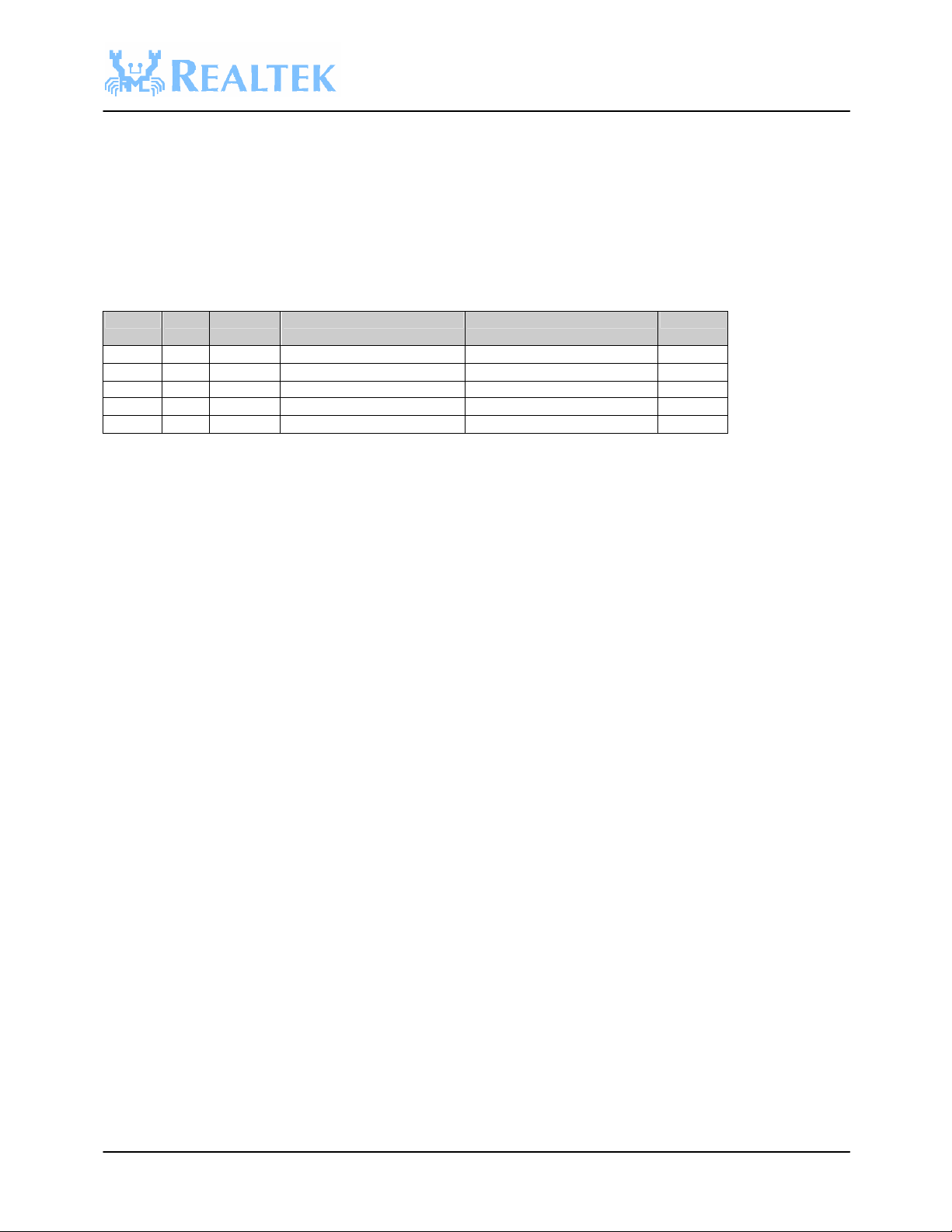
*A=Analog signal
*X=Not used .
3. Address Mapping
The RTL8181 supports up to 4 gigabytes of address space. The memory map of RTL8181 is managed by MMU, which will
translate the virtual address to physical address. The memory is segmented into four regions by its access mode and caching
capability as shown in following table.
Segment Size Caching Virtual address range Physical address range Mode
KUSEG 2048M cacheable 0x0000_0000-0x7fff_ffff set in TLB user/kernel
KSEG0 512M cacheable 0x8000_0000-0x9fff_ffff 0x0000_0000-0x1fff_ffff kernel
KSEG1 512M uncachable 0xa000_0000-0xbfff_ffff 0x0000_0000-0x1fff_ffff kernel
KSEG2 512M cacheable 0xc000_0000-0xfeff_ffff set in TLB kernel
KSEG2 512M cacheable 0xff00_0000-0xffff_ffff 0xff00_0000-0xffff_ffff kernel
The RTL8181 has two memory mapping modes: direct memory mapping and TLB (Translation Look-aside Buffer) address
mapping. When virtual address is located in the regions KSEG0, KSEG1 or higher half of KSEG2 segments, it physical
address will be mapped directly from virtual address with an offset. If virtual address used is in the regions of KUSEG or
lower half of KSEG2 segment, its physical address will be referred from TLB entry. RTL8181 contains 16 TLB entries, each
of which maps to a page, with read/write access, cache-ability and process id.
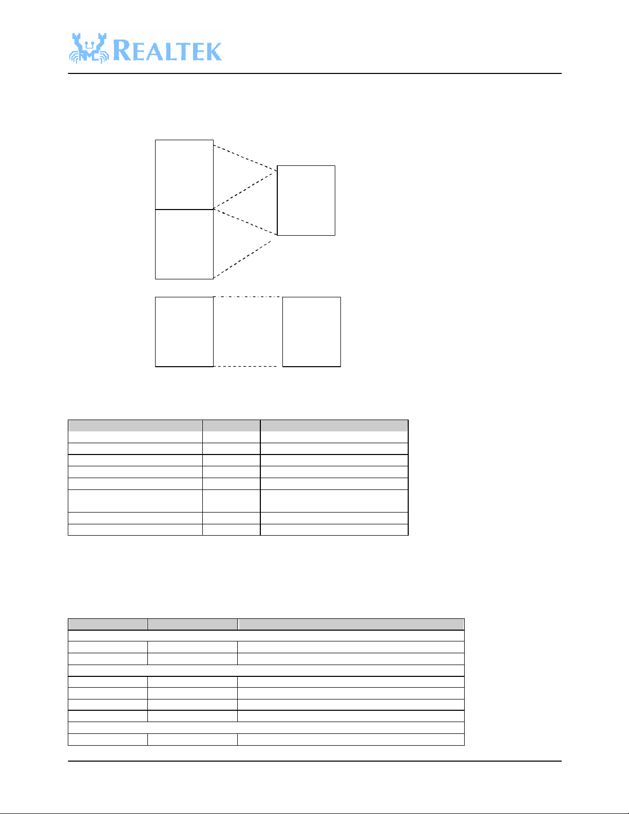
In RTL8181, SDRAM is mapped from physical address 0x0000_0000 to maximum 0x01ff_ffff (32M bytes). After reset,
RTL8181 will start to fetch instructions from physical address 0x1fc0_0000, the starting address of flash memory. The flash
memory is mapped from physical address 0x1fc0_0000 to maximum 0x1fff_ffff (4M bytes).
CONFIDENTIAL v1.0
12
Page 13
RTL8181
Cacheable
None
0x8000_0000
0x81ff_ffff
0xa000_0000
0xa1f
f_ffff
0x0000_0000
0x01ff_ffff
None
0xbfc0_0000
0xbfff_ffff
0x1fc0_0000
0x1fff_ffff
Memory map (without TLB):
Virtual Address
region
SDRAM
(32Mbyte)
cacheable
region
Physical Address
cacheable
region
Flash
(4Mbyte)
The memory map of RTL8181 I/O devices and registers are located in KSEG1 segment (uncacheable region). The following
table illustrates the address map:
Virtual address range Size (bytes) Mapped device
0xBD01_0000 – 0xBD01_0FFF 4K Special function registers (note)
0xBD01_1000 – 0xBD01_1FFF 4K Memory controller registers
0xBD20_0000 – 0xBD2F_FFFF 1M Ethernet0
0xBD30_0000 – 0xBD3F_FFFF 1M Ethernet1
0xBD40_0000 – 0xBD4F_FFFF 1M WLAN controller
0xBD50_0000 – 0xBD5F_FFFF 1M IO map address of PCI device
0xBD60_0000 – 0xBD6F_FFFF 1M Memory map address of PCI device
0xBD70_0000 – 0xBD77_FFFF 512K Configuration space of PCI device0
0xBD78_0000 – 0xBD7F_FFFF 512K Configuration space of PCI device1
NOTE: The special function includes interrupt control, timer, watchdog, UART, and GPIO.
4. Register Mapping
The following table displays the address mapping of the all registers:
Virtual Address Register Symbol Register Name
Interrupt Controller
0xBD01_0000 GIMR Global mask register
0xBD01_0004 GISR Global interrupt status register
GPIO
0xBD01_0040 PABDIR Port A/B direction register
0xBD01_0044 PABDATA Port A/B data register
0xBD01_0048 PBIMR Port B interrupt mask register
0xBD01_004C PBISR Port B interrupt register
Timer
0xBD01_0050 TCCNT Timer/Counter control register
CONFIDENTIAL v1.0
13
Page 14

RTL8181
0xBD01_0054 TCIR Timer/Counter interrupt register
0xBD01_0058 CBDR Clock division base register
0xBD01_005C WDTCNR Watchdog timer control register
0xBD01_0060 TC0DATA Timer/Counter 0 data register
0xBD01_0064 TC1DATA Timer/Counter 1 data register
0xBD01_0068 TC2DATA Timer/Counter 2 data register
0xBD01_006C TC3DATA Timer/Counter 3 data register
0xBD01_0070 TC0CNT Timer/Counter 0 count register
0xBD01_0074 TC1CNT Timer/Counter 1 count register
0xBD01_0078 TC2CNT Timer/Counter 2 count register
0xBD01_007C TC3CNT Timer/Counter 3 count register
UART
0xBD01_00C3 UART_RBR UART receiver buffer register
0xBD01_00C3 UART_THR UART transmitter holding register
0xBD01_00C3 UART_DLL UART divisor latch LSB
0xBD01_00C7 UART_DLM UART divisor latch MSB
0xBD01_00C7 UART_IER UART interrupt enable register
0xBD01_00CB UART_IIR UART interrupt ide ntification register
0xBD01_00CB UART_FCR UART FIFO control register
0xBD01_00CF UART_LCR UART line control register
0xBD01_00D3 UART_MCR UART modem control register
0xBD01_00D7 UART_LSR UART line status register
0xBD01_00DB UART_MSR UART modem status register
0xBD01_00DF UART_SCR UART scratch register
System Config
register
0xBD01_0100 BRIDGE_REG WLAN, Eherernet0, Ethernet1 and PCI bridge
0xBD01_0104 PLLMN_REG DLL M ,N parameter
0xBD01_0108 MEM_REG Memory clock setting
0xBD01_0109 CPU_REG CPU clock setting
Memory controller
0xBD01_1000 MCR Memory configuration register
0xBD01_1004 MTCR0 Memory timing configuration register 0
0xBD01_1008 MTCR1 Memory timing configuration register 1
Ethernet0
0xBD20_0000 ETH0_CNR1 Ethernet0 control register 0
0xBD20_0004 ETH0_ID Ethernet0 ID
0xBD20_000C ETH0_MAR Ethernet0 multicast register
0xBD20_0014 ETH0_TSAD Ethernet0 transmit starting address descriptor
0xBD20_0018 ETH0_RSAD Ethernet0 receive starting address descriptor
0xBD20_0020 ETH0_IMR Ethernet0 interrupt mask register
0xBD20_0024 ETH0_ISR Ethernet0 interrupt status register
0xBD20_0028 ETH0_TMF0 Ethernet 0 Type filter0 register
0xBD20_002C ETH0_TMF1 Ethernet 0 Type filter1 register
0xBD20_0030 ETH0_TMF2 Ethernet 0 Type filter2 register
0xBD20_0034 ETH0_TMF3 Ethernet 0 Type filter3 register
0xBD20_0038 ETH0_MII Ethernet0 MII access register
0xBD20_003C ETH0_CNR2 Ethernet0 control register 2
0xBD20_0040 ETH0_UAR Ethernet0 unicast address register
0xBD20_0080 ETH0_MPC Ethernet0 mismatch packet counter
0xBD20_0083 ETH0_TXCOL Ethernet0 transmit collision counter
0xBD20_0085 ETH0_RXER Ethernet0 receive error count
Ethernet1
0xBD30_0000 ETH1_CNR1 Ethernet1 control register 0
0xBD30_0004 ETH1_ID Ethernet1 ID
0xBD30_000C ETH1_MAR Ethernet1 multicast register
configuration register
CONFIDENTIAL v1.0
14
Page 15

RTL8181
0xBD30_0014 ETH1_TSAD Ethernet1 transmit starting address descriptor
0xBD30_0018 ETH1_RSAD Ethernet1 receive starting address descriptor
0xBD30_0020 ETH1_IMR Ethernet1 interrupt mask register
0xBD30_0024 ETH1_ISR Ethernet1 interrupt status register
0xBD30_0028 ETH1_TMF0 Ethernet1 type match filter 0
0xBD30_002C ETH1_TMF1 Ethernet1 type match filter 1
0xBD30_0030 ETH1_TMF2 Ethernet1 type match filter 2
0xBD30_0034 ETH1_TMF3 Ethernet1 type match filter 3
0xBD30_0038 ETH1_MII Ethernet1 MII access register
0xBD30_003C ETH1_CNR2 Ethernet1 control register 2
0xBD30_0080 ETH1_MPC Ethernet1 mismatch packet counter
0xBD30_0083 ETH1_TXCOL Ethernet1 transmit collision counter
0xBD30_0085 ETH1_RXER Ethernet1 receive error count
WLAN controller
0xBD40_0000 WLAN_ID WLAN ID
0xBD40_0008 WLAN_MAR WLAN multicast register
0xBD40_0018 WLAN_ TSFTR WLAN timing synchronization function timer register
0xBD40_0020 WLAN_ TLPDA WLAN transmit low priority descriptors start address
0xBD40_0024 WLAN_ TNPDA WLAN transmit normal priority descriptors start address
0xBD40_0028 WLAN_ THPDA WLAN transmit high priority descriptors start address
0xBD40_002C WLAN_ BRSR WLAN basic rate set register
0xBD40_002E WLAN_ BSSID WLAN basic service Set ID
0xBD40_0037 WLAN_ CR WLAN command register
0xBD40_003C WLAN_IMR WLAN interrupt mask register
0xBD40_003E WLAN_ISR WLAN interrupt status register
0xBD40_0040 WLAN_TCR WLAN transmit configuration register
0xBD40_0044 WLAN_RCR WLAN receive configuration register
0xBD40_0048 WLAN_TINT WLAN timer interrupt register
0xBD40_004C WLAN_ TBDA WLAN transmit beacon descriptor start address
0xBD40_0050 WLAN_CR WLAN command register
0xBD40_0051 WLAN_CONFIG0 WLAN configuration register 0
0xBD40_0053 WLAN_CONFIG2 WLAN configuration register 2
0xBD40_0054 WLAN_ANAPARM WLAN analog parameter
0xBD40_0058 WLAN_MSR WLAN media status register
0xBD40_0059 WLAN_CONFIG3 WLAN configuration register 3
0xBD40_005A WLAN_CONFIG4 WLAN configuration register 4
0xBD40_005B WLAN_TESTR WLAN test mode register
0xBD40_005F WLAN_SCR WLAN security configuration register
0xBD40_0070 WLAN_BCNITV WLAN beacon interval register
0xBD40_0072 WLAN_ATIMWND WLAN ATIM window register
0xBD40_0074 WLAN_BINTRITV WLAN beacon interrupt interval register
0xBD40_0076 WLAN_ATIMTRITV WLAN ATIM interrupt interval register
0xBD40_0078 WLAN_PHYDELAY WLAN PHY delay register
0xBD40_007A WLAN_CRC16ERR WLAN CRC16 error count
0xBD40_007C WLAN_PHYADDR WLAN PHY address register
0xBD40_007D WLAN_PHYDATAW WLAN write data to PHY
0xBD40_007E WLAN_PHYDATAR WLAN read data from PHY
0xBD40_0080 WLAN_PHYCFG WLAN PHY configuration register
0xBD40_0090 WLAN_DK0 WLAN default key 0 register
0xBD40_00A0 WLAN_DK1 WLAN default key 1 register
0xBD40_00B0 WLAN_DK2 WLAN default key 2 register
0xBD40_00C0 WLAN_DK3 WLAN default key 3 register
0xBD40_00D8 WLAN_CONFIG5 WLAN configuration register 5
0xBD40_00D9 WLAN_TPPOLL WLAN transmit priority polling register
0xBD40_00DC WLAN_CWR WLAN contention window register
0xBD40_00DE WLAN_RETRYCTR WLAN retry count register
0xBD40_00E4 WLAN_RDSAR WLAN receive descriptor start address register
CONFIDENTIAL v1.0
15
Page 16

RTL8181
mode,the MEM
0xBD40_0100 WLAN_KMAR WLAN key map address register
0xBD40_0106 WLAN_KMKEY WLAN key map key value
0xBD40_0116 WLAN_KMC WLAN key map configuration
5. System Configuration
GPIO pin for system configuration
GPIOB pin Power on Latch Value Operating setting Power on default
9-6 1111
other values are reserved
11,10 01
11
other values are reserved
13 1
0
15-14 Reserved Reserved
1,0 Reserved Reserved 1,1
System Control Register Set
Virtual address Size (byte) Name Description
0xBD01_0100 4 BRIDGE_R
EG
0xBD01_0104 4 PLLMN_R
EG
0xBD01_0108 1 MEM_REG RTL8181 Memory clock rate
0xBD01_0109 1 CPU_REG RTL8181 CPU clock rate
Bridge Control Register (BRIDGE_REG)
Since the Lexra bus clock rate is fast than the network device, it needs a bus bridge between the CPU and device (i.e., Ethernet
and Wireless LAN controller). Also, this bridge is existed between CPU and PCI bridge.
Bit Bit Name Description R/W InitVal
2-0 NIC0CKR Bus clock to NIC0 clock ratio. 001= 1:2,
011=1:4,101=1:6,111=1:8 ,other value
reserved. The NIC0 and NIC1 maximum clock
is 50MHz.
3 NIC0CKREN NIC0CKR write enable R/W 0
6-4 - Reserved - 7 DISNIC0B Disable NIC0,0 enable NIC0, 1 disable NIC0 R/W 0
10-8 NIC1CKR Bus clock to NIC1 clock ratio. 001= 1:2,
011=1:4,101=1:6,111=1:8 ,other value
reserved
11 NIC1CKREN NIC0CKR write enable R/W 0
14-12 - Reserved R/W 0
15 DISNIC1B Disable NIC1,0 enable NIC1, 1 disable NIC1 R/W 0
18-16 PCICLKR Bus clock to PCI clock ratio. 000=1:1,001=
1:2,010=1:3,011=1:4,100=1:5,101=1:6,110=1:
7,111=1:8. The PCI maximum clock is
50MHz.
19 PCICKREN PCICLKR write enable R/W 0
20 LXPCI The external Bus is PCI or Lexra(debug
mode).0 Lexra, 1 PCI.
21 PCI2ENB The second PCI bus enable. 0 enable second
PCI device,1 disable second PCI device
22 Reserved
CONFIDENTIAL v1.0
CPU=200,MEM=100 if
Memory use asynchronous
mode
JTAG mode
Normal mode (wlan LED)
Memory clock use
asynchronous mode.
Synchronous
clock same as CPU clock
WLAN, Eherernet0, Ethernet1 and PCI
bridge configuration register
RTL8181 DPLL parameter
R/W 011
R/W 011
R/W 101
R/W 1
R/W 1
16
1,1,1,1
1,1
1
Page 17
RTL8181
Bus clock to WLAN clock ratio. 000=1:1,001=
23 DISPCIB Disable PCI bridge,0 enabe PCI bridge,1
disable PCI bridge
26-24 WLANCKR
1:2,010=1:3,011=1:4,100=1:5,101=1:6,110=1:
7,111=1:8. The WLAN maximum clock is
40MHz.
27 WLANCKREN WLANCKR write enable R/W 0
30-28 Reserved - - 31 DISWLANB Disable WLAN, 0 enabe WLAN,1 disable
WLAN
R/W 0
R/W 101
R/W 0
DPLL M,N parameter Register (PLLMN_REG)
The DPLL clock rate is setting by this equation:
44MHz*(M+1)/(N+1)
Bit Bit Name Description R/W InitVal
4-0 NDIV DPLL N parameter R/W 00011
7-5 Reserved - - 13-8 MDIV DPLL M parameter R/W 10011
14 MNEN MDIV and NDIV write enable,0 disable ,1
enable
31-15 Reserved - - 0
Memory parameter Register (MEM_REG)
Bit Bit Name Description R/W InitVal
2-0 MEMDIV MEM clock ,000:DPLL/1, 001: DPLL/1.5,
010: DPLL/2,011:DPLL/2.5,
100:DPLL/3,101:DPLL/4, 110:DPLL/6,
111:DPLL/8
3 MEMDIVEN Enable MEMDIV writw,0 disable ,1 enable R/W 0
7-4 Reserved - - -
CPU parameter Register (CPU_REG)
Bit Bit Name Description R/W InitVal
2-0 CPUDIV CPU clock ,000:DPLL/1, 001: DPLL/1.5, 010:
DPLL/2,011:DPLL/2.5,
100:DPLL/3,101:DPLL/4, 110:DPLL/6,
111:DPLL/8
3 CPUDIVEN Enable CPUDIV writw,0 disable ,1 enable R/W 0
7-4 Reserved - - -
R/W 0
R/W 000
R/W 000
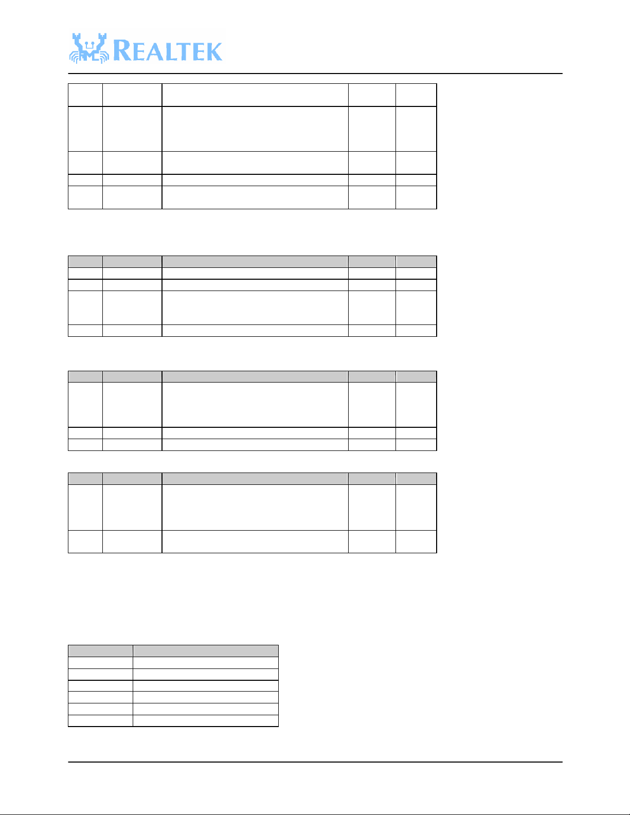
6. Interrupt Controller
RTL8181 provides six hardware-interrupt inputs IRQ0-IRQ5 internally. Some devices will share the same IRQ signal.
Following table displays the IRQ map used by devices:
IRQ Number Interrupt Source
0 Timer/Counter interrupt
1 GPIO/LBC interrupt
2 WLAN interrupt
3 UART/PCI interrupt
4 Ethernet0 interrupt
5 Ethernet1 interrupt
CONFIDENTIAL v1.0
17
Page 18
RTL8181
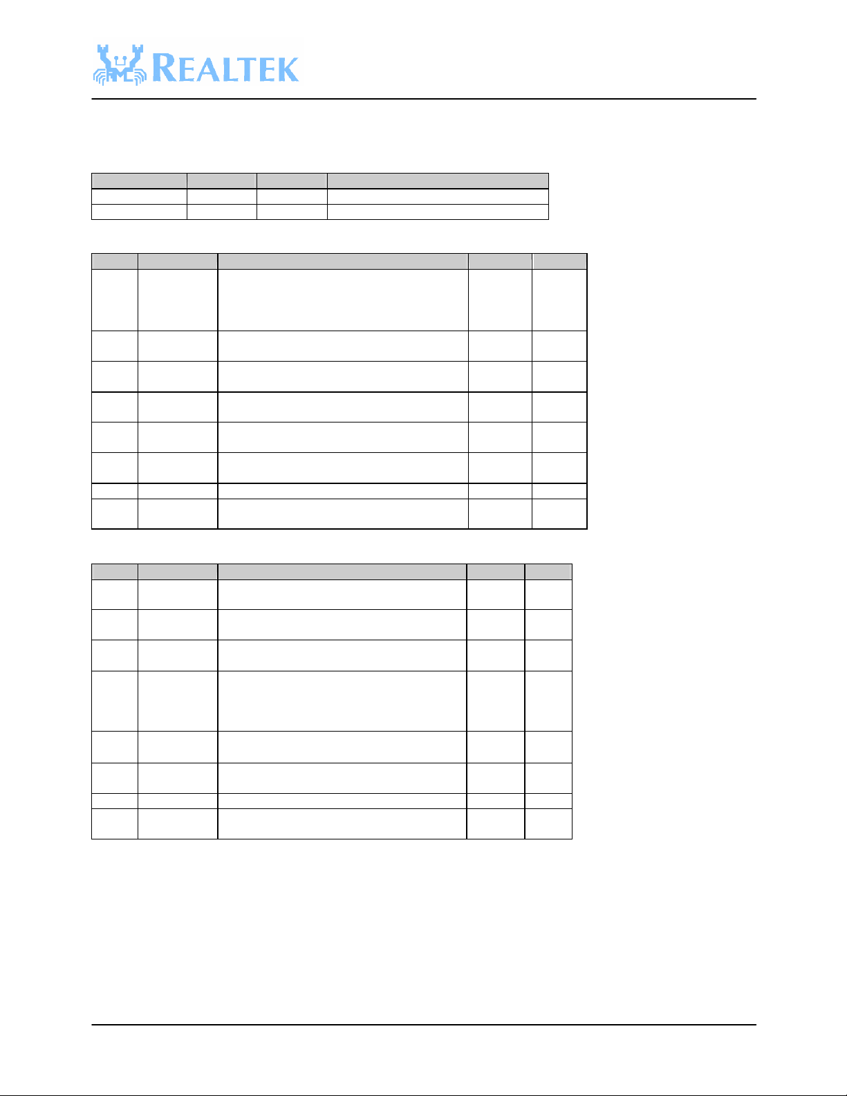
There are two registers for the interrupt control. The GIMR register can enable/disable the interrupt source. The GISR shows
the pending interrupt status.
Interrupt Control Register Set
Virtual address Size (byte) Name Description
0xBD01_0000 2 GIMR Global interrupt mask register
0xBD01_0004 2 GISR Global interrupt status register
Global Interrupt Mask Register (GIMR)
Bit Bit Name Description R/W InitVal
0 TCIE Timers/Counters interrupt enable.
0: Disable, 1: Enable
1 GPIOIE GPIO interrupt enable.
0: Disable, 1: Enable
2 WLAIE WLAN controller interrupt enable.
0: Disable, 1: Enable
3 UARTIE UART interrupt enable.
0: Disable 1: Enable
4 ETH0IE Ethernet0 interrupt enable.
0: Disable, 1: Enable
5 ETH1IE Ethernet1 interrupt enable .
0: Disable, 1: Enable
6 PCIIE PCI interrupt enable.
0: Disable, 1: Enable
7 Reserved
8 LBC1E LBC time-out interrupt enable.
0: Disable, 1: Enable
R/W 0
R/W 0
R/W 0
R/W 0
R/W 0
R/W 0
R/W 0
R/W 0
Global Interrupt Status Register (GISR)
Bit Bit Name Description R/W InitVal
0 TCIP Timers/Counters interrupt pending flag.
0: no pending, 1: pending
1 GPIOIP GPIO interrupt pending flag.
0: no pending, 1: pending
2 WLAIP WLAN controller interrupt pending flag.
0: no pending, 1: pending
3 UARTIP UART I interrupt pending flag.
0: no pending, 1: pending
4 ETH0IP Ethernet0 interrupt pending flag.
0: no pending, 1: pending
5 ETH1IP Ethernet1 interrupt pending flag.
0: no pending, 1: pending
6 PCIIP PCI interrupt pending flag.
0: no pending, 1: pending
7 Reserved
8 LBCIP LBC time-out interrupt pending flag.
0: no pending, 1: pending
R 0
R 0
R 0
R 0
R 0
R 0
R 0
R 0
7. Memory Controller
RTL8181 provides a memory control module that could access external asynchronous SDRAM and flash memory.
RTL8181 could interface to PC100 or PC133-compliant SDRAM, and supports with auto-refresh mode, which requires
4096-cycle refresh in 64 ms. The SDRAM could be accessed in two banks (CS0#, and CS1#), and its size and timing are
configurable in register. The data width of SDRAM could be chosen as 16-bit or 32-bit in register as well. If 32-bit is
configured, 2 banks of 16-bit SDRAM may be used to expand its data width to 32 bits or use one bank of 32-bit SDRAM is
allowable.
CONFIDENTIAL v1.0
18
Page 19
RTL8181
is the same as CPU clock. 0:memory clock following the power on latch
Besides, RTL8181could also supports two banks (F_CS0# and F_CS1#) access for flash memory. The system will always boot
up from bank 0. The boot bank is mapped to KSEG1 and its beginning physical address at 0xBFC0_0000 (physical address:
0x1FC0_0000). Bank 1 flash memory will be mapped to the address “0x1FC0_000 + flash size”. The flash size is configurable
from 1M to 8M bytes for each bank. If flash size set to 4M or 8M the 0xBFC0_0000 still map the first 4M bytes of flash.
There will have a new memory mapping from 0xBE00_0000. The 0xBE00_0000 mapped to the bank 0 byte 0.
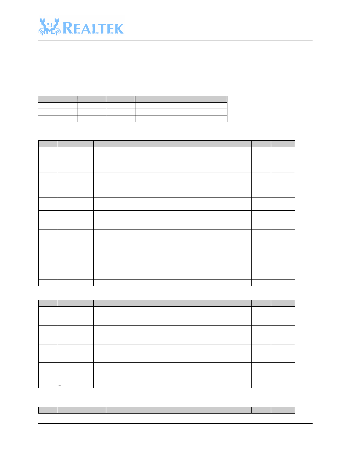
Memory Configuration Register Set
Virtual address Size (byte) Name Description
0xBD01_1000 4 MCR Memory Configuration Register
0xBD01_1004 4 MTCR0 Memory Timing Configuration Register 0
0xBD01_1008 4 MTCR1 Memory Timing Configuration Register 1
Note: These three registers should be accessed in double word.
Memory Configuration Register (MCR)
Bit Bit Name Description R/W InitVal
.31-30 FLSIZE Flash size respective to one bank (byte).
00: 1M, 01: 2M, 10: 4M, 11:8M
29-28 SDRSIZE SDRAM size respective to one bank (bit).
00: 512Kx16x2, 01: 1Mx16x4, 10: 2Mx16x4, 11:Reserved
27 CAS CAS Latency
0: Latency=2, 1: Latency=3
26-25 FLBK0BW Flash bank 0 bus width.
01: 16 bit
24-23 FLBK1BW Flash bank 1 bus width
00 11 10: reserved, 01: 16 bit
22-21 - Reserved
20 SDBUSWID SDRAM bus width
0: 16 bit, 1: 32 bit
19 MCK2LCK Memory clock mode.Power on latch from GPIOB[13].1:Memory clock
R/W 11
R/W 01
WR 0
R
W/R 01
W/R 1
0
R
from SYSCFG[3-0].
18-16 BUSCLK Bus Clock to control auto-refresh timing
000:200, 001:100, 010:50, 011:25, 100:12.5, 101:6.25
110: 3.125, 111: 1.5625 MHz
15-0 Reserved Must be set to bit value 00. R/W 00
R/W 000
Memory Timing Configuration Register 0 (MTCR0)
Bit Bit Name Description R/W InitVal
31-28 CE0T_CS The timing interval between F_CE0# to WR#
Basic unit, 2*clock cycle
“0000” means 1 unit (2 clock cycles)
27-24 CE0T_WP The timing interval for WR# to be pulled-low
Basic unit, 2*clock cycle
“0000” means 1 unit (2 clock cycles)
23-20 CE1T_CS The timing interval between F_CE1# to WR#
Basic unit, 2*clock cycle
“0000” means 1 unit (2 clock cycles)
19-16 CE1T_WP The timing interval for WR# to be pulled-low
Basic unit, 2*clock cycle
“0000” means 1 unit (2 clock cycles)
15-0 - Reserved
Note: The clock cycle is based memory clock.
Memory Timing Configuration Register 1 (MTCR1)
Bit Bit Name Description R/W InitVal
R/W 1111
R/W 1111
R/W 1111
R/W 1111
CONFIDENTIAL v1.0
19
Page 20
RTL8181
12-10 CE23T_RP=T_RCD T_RP and T_RCD timing parameter
Basic unit, 1*clock cycle
“0000” means 1 unit (1 clock cycle)
9-5 CE23T_RAS T_RAS timing parameter
Basic unit, 1*clock cycle
“0000” means 1 unit (1 clock cycle)
4-0 CE23T_RFC T_RFC timing parameter for refresh interval
Basic unit, 1*clock cycle
“0000” means 1 unit (1 clock cycle)
Note: The clock cycle is based memory clock.
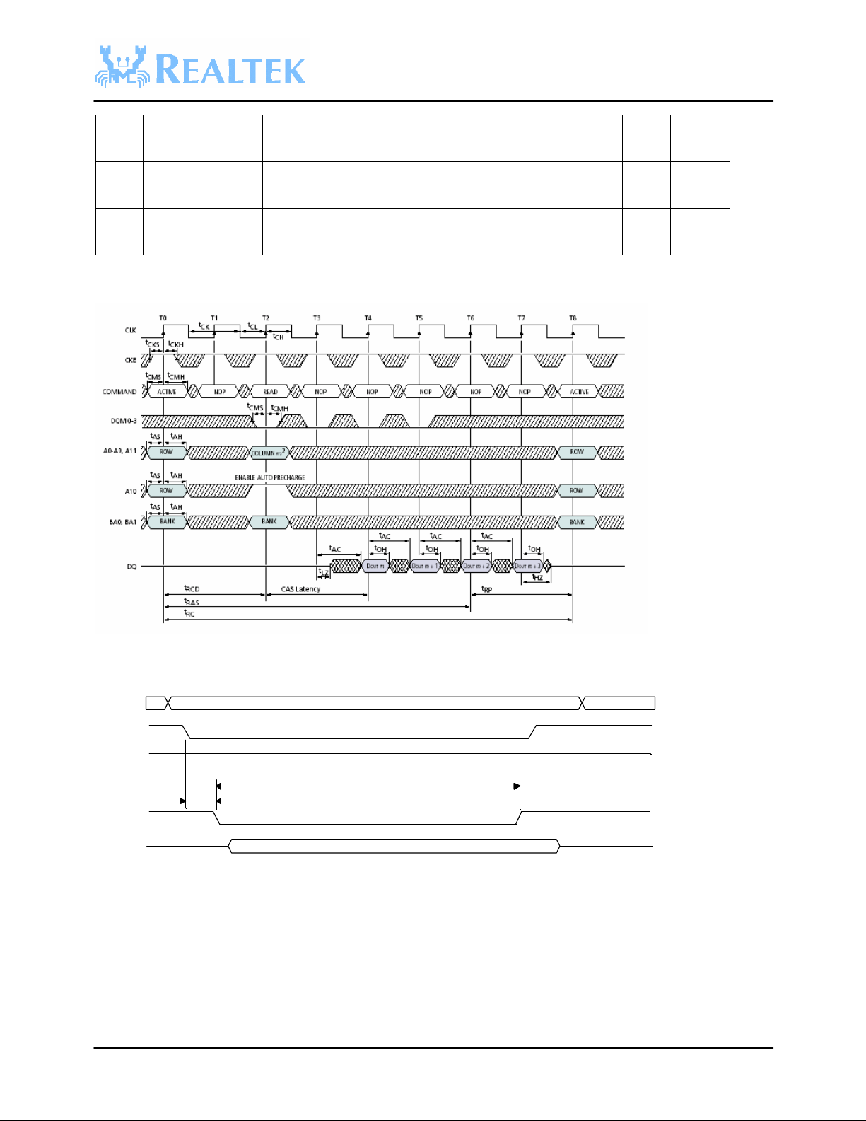
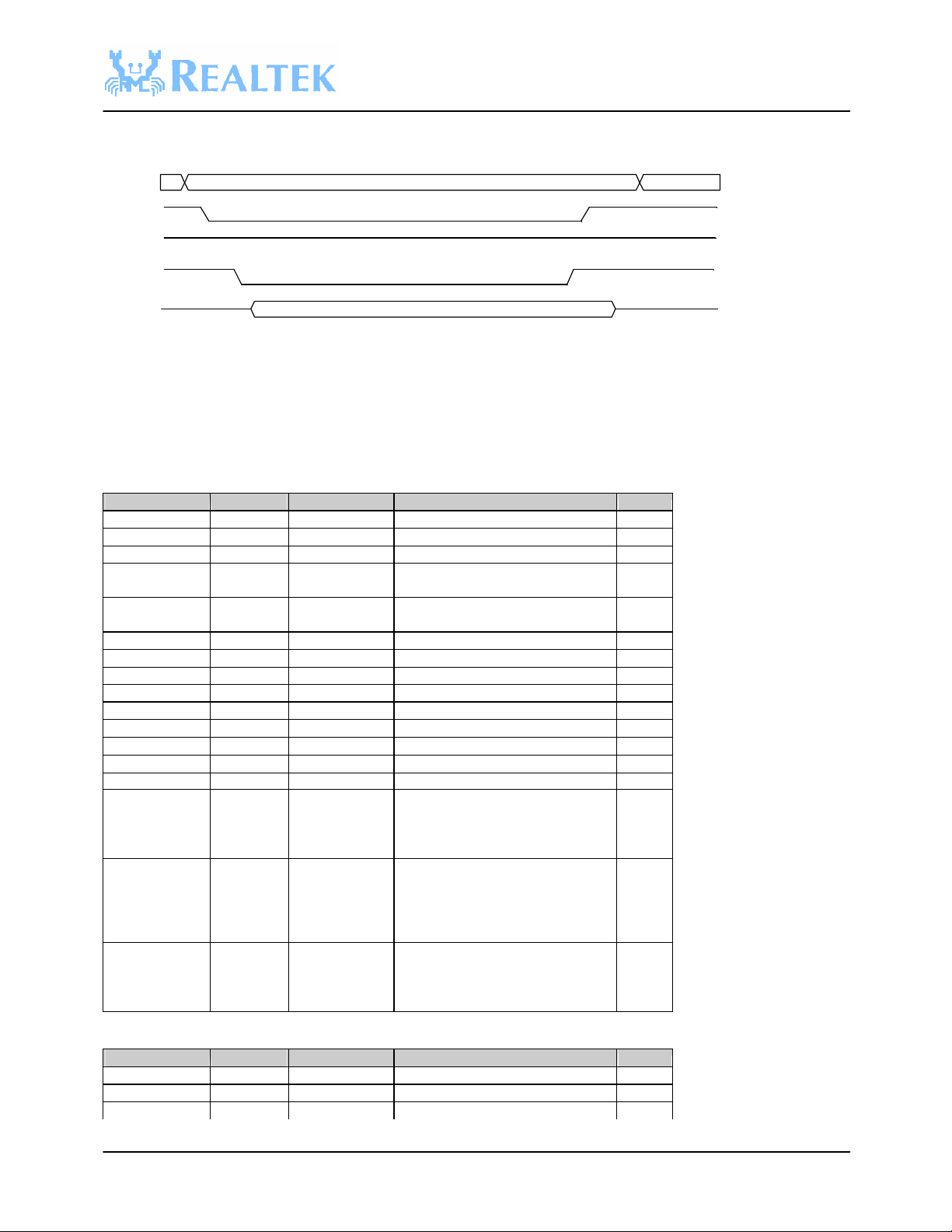
The SDRAM timing:
R/W 111
R/W 11111
R/W 11111
The write access timing of flash memory:
A[20..0]
F_CE0#
OE#
Tcs
WR#
D[n..0]
TwpTwp
CONFIDENTIAL v1.0
20
Page 21
RTL8181
The read access timing of flash memory:
A[20..0]
F_CE0#
WE#
OE#
D[n..0]
8. Ethernet Controller
There are two 10/100M Ethernet MAC embedded in RTL8181. The Ethernet device has bus master capability, which will
move packets between SDRAM and Ethernet controller through DMA mechanism. Thus, it could offload the CPU loading and
get better performance. Besides, it also supports full-duplex operation, making possible 200Mbps bandwidth at no additional
cost.
Ethernet 0 Register Set (LAN PORT)
Virtual Address Size (byte) Name Description Access
0xBD20_0000 4 ETH0_CNR1 Control register 1 R/W
0xBD20_0004 6 ETH0_ID NIC ID R/W
0xBD20_000C 8 ETH0_MAR Multicast register R/W
0xBD20_0014 4 ETH0_TSAD Transmit Starting Logic Address of
Descriptor
0xBD20_0018 4 ETH0_RSAD Receive Starting Logic Address of
Descriptor
0xBD20_0020 2 ETH0_IMR Ethernet0 Interrupt Mask Register R/W
0xBD20_0024 2 ETH0_ISR Ethernet0 Interrupt Status Register R/W
0xBD20_0028 4 ETH0_TMF0 Type match filter 0 register R/W
0xBD20_002C 4 ETH0_TMF1 Type match filter 1 register R/W
0xBD20_0030 4 ETH0_TMF2 Type match filter 2 register R/W
0xBD20_0034 4 ETH0_TMF3 Type match filter 3 register R/W
0xBD20_0038 4 ETH0_MII MII access register R/W
0xBD20_003C 4 ETH0_CNR2 NIC control register 2 R/W
0xBD20_0040 16 ETH0_UAR Unicast address filter register R/W
0xBD20_0080 3 ETH0_MPC Indicates the number of packets
discarded due to rx FIFO overflow.
It is a 24-bit counter. It is cleared to
zero by read command.
0xBD20_0084 2 ETH0_TXCOL Transmit collision counter. This
16-bit counter increments by 1 for
every collision event. It rolls over
when becomes full. It is cleared to
zero by read command.
0xBD20_0088 2 ETH0_RXER Receive error count. This 16-bit
counter increments by 1 for each
valid packet received . It is cleared
to zero by read command.
Ethernet 1 Register Set (WAN PORT)
Virtual Address Size (byte) Name Description Access
0xBD30_0000 4 ETH1_CNR1 Control register 1 R/W
0xBD30_0004 6 ETH1_ID NIC ID R/W
0xBD30_000C 8 ETH1_MAR Multicast register R/W
R/W
R/W
R
R
R
CONFIDENTIAL v1.0
21
Page 22

RTL8181
0xBD30_0014 4 ETH1_TSAD Transmit Starting Logic Address of
Descriptor
0xBD30_0018 4 ETH1_RSAD Receive Starting Logic Address of
Descriptor
0xBD30_0020 2 ETH1_IMR Ethernet0 Interrupt Mask Register R/W
0xBD30_0024 2 ETH1_ISR Ethernet0 Interrupt Status Register R/W
0xBD30_0028 4 ETH1_TMF0 Type match filter 0 register R/W
0xBD30_002C 4 ETH1_TMF1 Type match filter 1 register R/W
0xBD30_0030 4 ETH1_TMF2 Type match filter 2 register R/W
0xBD30_0034 4 ETH1_TMF3 Type match filter 3 register R/W
0xBD30_0038 4 ETH1_MII MII access register R/W
0xBD30_003C 4 ETH1_CNR2 NIC control register 2 R/W
0xBD30_0080 3 ETH1_MPC Indicates the number of packets
discarded due to rx FIFO overflow.
It is a 24-bit counter. It is cleared to
zero by read command.
0xBD30_0084 2 ETH1_TXCOL Transmit collision counter. This
16-bit counter increments by 1 for
every collision event. It rolls over
when becomes full. It is cleared to
zero by read command.
0xBD30_008C 2 ETH1_RXER Receive error count. This 16-bit
counter increments by 1 for each
valid packet received . It is cleared
to zero by read command.
R/W
R/W
R
R
R
Ethernet Control Register 1 (ETH0_CNR1, ETH1_CNR1)
Bit Bit Name Description R/W InitVal
31-29 RXBLEN Rx Burst length on Lexra bus.
000 - 010 = 64 bytes
28-26 TXBLEN Tx Burst length on Lexra bus.
000 = 16 bytes
001 = 32 bytes
010 = 64 bytes
25 FIFOAddrPtr FIFO Address Pointer: (Realtek internal use only
to test FIFO SRAM)
0: Both Rx and Tx FIFO address pointers are
updated in ascending way from 0 and upwards.
The initial FIFO address pointer is 0.
1: Both Rx and Tx FIFO address pointers are
updated in descending way from 1FFh and
downwards. The initial FIFO address pointer is
1FFh.
24 TDFN Tx Descriptor Fetch Notify. Set this bit to notify
the NIC to fetch the Tx descriptors. The NIC will
clear this bit automatically after all packets have
been transmitted. Writing 0 to this bit has no
effect.
20 RST Reset. A soft reset which disable the transmitter
and receiver, re-initializes the FIFOs, and buffer
pointer to the initial value.
19 RE Receiver enable. R/W 0
18 TE Transmitter enable. R/W 0
17 TxFCE Transmit flow control enable. R/W 0
16 RxFCE Receive flow control enable R/W 0
15 Reserved 0
14 RxVLAN Receive VLAN un-tagging enable R/W 0
13 RxChkSum Receive checksum offload enable R/W 0
R/W 000
R/W 000
R/W 0
W 0
W 0
CONFIDENTIAL v1.0
22
Page 23

RTL8181
This bit is effective
state because a pause packet received. Reset, when
12 FSWInt Forced software interrupt.
Writing 1 to this bit will trigger an interrupt, and
the SWIP bit will be set.
The NIC will clear this bit automatically after
SWIP bit is cleared.
Writing 0 to this bit has no effect.
11-10 LBK[1:0] Loopback test. Setting both bits will route all
transmit traffic from Tx FIFO to Rx FIFO
00: normal operation
01, 10: reserved
11: loopback mode
9 NoCRC No CRC.
0: CRC appended
1: no CRC appended
8 AER Accept error packets R/W 0
7 AB Accept Broadcast packets R/W 0
6 AM Accept Multicast packets R/W 0
5 APM Accept Physical address Matched packets R/W 0
4 AAP Accept All Physical packets
3 ATM Accept Type match packets. This bit enables the
qualification of types of received packets.
2 AR Accept runt packets R/W 0
1 ALEN Accept length specific packets.
when ATM bit is set.
0: filter length specific packets.
1: accept length specific packets.
W
R/W 00
R/W 0
R/W 0
R/W 0
R/W 0
Ethernet Control Register 2 (ETH0_CNR2, ETH1_CNR2)
Bit Bit Name Description R/W InitVal
16 UAEN Unicast address filter enable (note).
0: disabled. 1: enabled.
15 TXPON Send Pause On packet. Write “1” to send Pause
On packet.
14 TXPOFF Send Pause Off packet. Write “1” to send Pause
Off packet.
13 TXPF Send Pause flag. Set, when NIC sends Pause-On
packet. Reset, when NIC sends Pause-Off packet.
12 RXPF Receive Pause Flag: Set, when NIC is in backoff
R/W 0
W 0
W 0
R 0
R 0
pause state is clear.
11-8 PTMASK[3:0] Pause time mask. These bits mask the most
significant four bits of pause time 0xFFFF used
for a PAUSE packet. For example, if
PTMASK[3:0] is set to 0x01, a PAUSE packet
with pause time 0x1FFF will be sent when
descriptor unavailable condition occurs.
6-4 IFG[2:0] InterFrameGap Time: This field allows the user to
adjust the interframe gap time longer than the
standard: 9.6 us for 10Mbps, 960 ns for 100Mbps.
The time can be programmed from 9.6 us to 14.4
us (10Mbps) and 960ns to 1440ns (100Mbps).
The formula for the inter frame gap is
011: 9.6us/ 960ns
100: 9.6+4*0.1us/ 960+4*10ns
101: 9.6+8*0.1us/ 960+8*10ns
110: 9.6+12*0.1us/ 960+12*10ns
111: 9.6+16*0.1us/ 960+16*10ns
CONFIDENTIAL v1.0
R/W 1111
R/W 011
23
Page 24

RTL8181
Total retries = 16 + (TXRR * 16)
000: 9.6+20*0.1us/ 960+20*10ns
001: 9.6+24*0.1us/ 960+24*10ns
010: 9.6+48*0.1us/ 960+48*10ns
3-0 TXRR[3:0] Tx Retry Count: These are used to specify
additional transmission retries in multiple of
16(IEEE 802.3 CSMA/CD retry count). If the
TXRR is set to 0, the transmitter will re-transmit
16 times before aborting due to excessive
collisions. If the TXRR is set to a value greater
than 0, the transmitter will re-transmit a number of
times equals to the following formula before
aborting:
The TER bit in the ISR register or transmit
descriptor will be set when the transmission fails
and reaches to this specified retry count.
Note: Bit UAEN is only existed in ETH0_CNR2 register.
R/W 0
Unicast Address Filter Register (ETH0_UAR)
Bit Bit Name Description R/W InitVal
127-0 UARTBL Unicast address hash table. If the ‘n’ bit value is
set ‘1’, it implies the receiving frames which hash
value with ‘n’ will be indicated.
Interrupt Mask Register (ETH0_IMR, ETH1_IMR)
Bit Bit Name Description R/W InitVal
9 LINKCHGIE Link status changed interrupt enable R/W 0
8 RERIE Rx error interrupt enable R/W 0
7 TERIE Tx error interrupt enable R/W 0
6 ROKIE ROK interrupt enable. A descriptor reception is
completed successfully.
5 TOKIE TOK interrupt enable. A descriptor transmission is
completed successfully.
4 RFOVWIE Rx FIFO overflow interrupt enable R/W 0
3 RDUIE Rx descriptor unavailable interrupt enable. Set
when the Rx Descriptors have been exhausted.
2 Reserved
1 TDUIE Tx descriptor unavailable interrupt enable R/W 0
0 SWIE Software interrupt enable R/W 0
R/W 0
R/W 0
R/W 0
R/W 0
Interrupt Status Register (ETH0_ISR, ETH1_ISR)
Bit Bit Name Description R/W InitVal
9 LINKCHGIP Link status changed interrupt pending flag. Write
“1” to clear the interrupt.
8 RERIP Rx error interrupt pending flag. Write “1” to clear
the interrupt.
7 TERIP Tx error interrupt enable flag. Write “1” to clear
the interrupt.
6 ROKIP ROK interrupt pending. A descriptor reception is
completed successfully. Write “1” to clear the
interrupt.
5 TOKIP TOK interrupt pending. A descriptor transmission
is completed successfully. Write “1” to clear the
interrupt.
4 RFOVWIP Rx FIFO overflow interrupt pending Write “1” to
clear the interrupt..
3 RDUIP Rx descriptor unavailable interrupt pending. Set
when the Rx Descriptors have been exhausted.
Write “1” to clear the interrupt and it also trigger
CONFIDENTIAL v1.0
24
R/W 0
R/W 0
R/W 0
R/W 0
R/W 0
R/W 0
R/W 0
Page 25

RTL8181
0 = auto mode. The NIC controls MDC and MDIO
controls MDC and
Link status. This bit reflects the link status from its
NIC to send PAUSE 0x0000 packet.
2 Reserved
1 TDUIP Tx descriptor unavailable interrupt pending flag.
Write “1” to clear the interrupt.
0 SWIP Software interrupt pending flag. Write “1” to clear
the interrupt.
R/W 0
R/W 0
MII Access Register (ETH0_MII, ETH1_MII)
Bit Bit Name Description R/W InitVal
31-22 - Reserved
21 MMIMODE Mode of MII management interface. (Realtek
internal use only to test 3-port switch)
pins. Setting this bit will trigger an
auto- negotiation if DisNway bit is cleared.
1 = manual mode. The software
MDIO pins.
20-16 PHYAD[4:0] PHY address. R/W 0x01
15 LinkCtrl Link control.
0: force link down.
1: force link up.
14 DplxCtrl Duplex control. When DuplexCtrl bit is cleared,
this bit is read only. The NIC will poll its local
PHY regularly. This bit will reflect the result of
auto- negotiation from its local PHY. If FDuplex is
set, this bit is writable. The software may program
the bit and force the MII operates in full-duplex or
half-duplex mode.
0: Force half-duplex mode.
1: Force full-duplex mode.
13 SpdCtrl Speed control.
0: 10Mbps
1: 100Mbps.
12 FlCtrl Flow control.
0:disable flow control.
1: enable flow control.
11 LinkSt
local PHY.
0: link down
1: link up
10 DuplexSt Duplex status. This bit reflects the duplex status
from its local PHY.
0: half duplex
9 SpeedSt Speed status. This bit reflects the link speed from
its local PHY.
0: 10Mbps
1: 100Mbps
8 FlCtrlSt Flow control status
0: flow control disabled
1: flow control enabled.
7-5 - Reserved
4 DisNway Disable N-way
0: auto- negotiation mode.The local PHY will
advertise its capability per the settings of
DplxCtrl, SpdCtrl, and FlCtrl bits.
1: forced mode (disable N-way). The software
may force MII operating mode by writing the
corresponding value to the DplxCtrl, LinkCtrl,
SpdCtrl,FlCtrl bits.
CONFIDENTIAL v1.0
25
R/W 0
R/W 0
R/W 1
R/W 1
R/W 0
R 0
R 0
R 0
R 0
R/W 0
Page 26
RTL8181
a Clock: This bit reflects the state
R
V
A command bit. UDP checksum offload. Driver sets this bit to ask NIC
3 MDM Management Data Mode:
0: MDIO pin is input. MDI bit reflects the state of
MDIO pin. The default value is "0".
1: MDIO pin is output, and the state of MDIO pin
reflects with MDO bit.
2 MDO MII Management Data-OUT: Used by the NIC to
write data to the MDIO pin.
1 MDI MII Management Data-IN: Used by the NIC to
read data from the MDIO pin.
0 MDC Management Dat
of MDC pin.
R/W 0
R/W X
R X
R/W 0
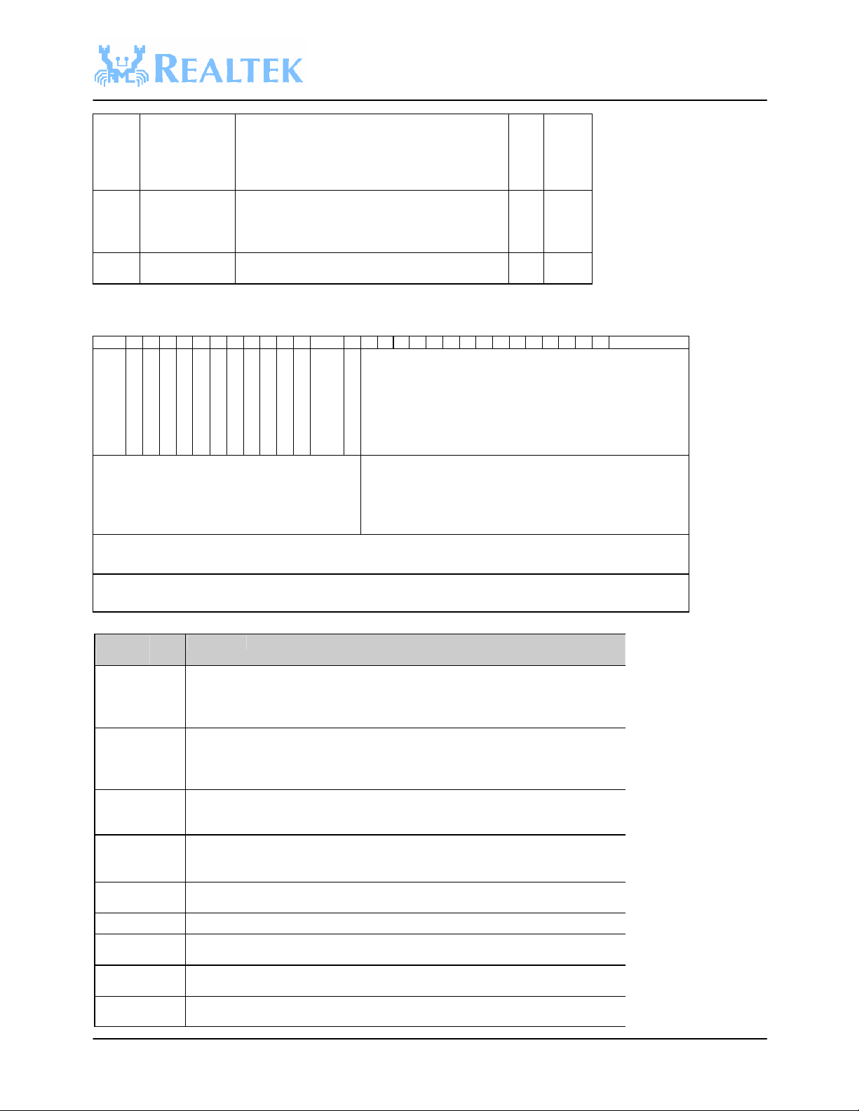
Transmit Descriptor
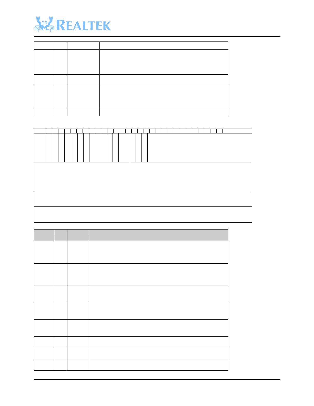
Tx Descriptor Format (before transmitting, OWN=1, LGSEN=0, Tx command mode 1)
31 30 29 28 27 26 25 24 23 22 21 20 19 18 17 16 15 14 13 12 11 10 9 8 7 6 5 4 3 2 1 0
O
FS LS L
W
N
=
1
R
R
R
R
R
R
R
R
I
U
T
G
E
E
E
E
E
E
E
E
P
D
C
S
S
S
S
S
S
S
S
S
C
P
P
E
V
V
V
V
V
V
V
S
C
C
N
=
0
RESV
S
S
TAGC
Frame_Length
VLAN_TAG
Offset 0
Offset 4
TX_BUFFER_ADDRESS
Dummy
Offset 8
Offset 12
Byte
Offset#
0 31 OWN When set, indicates that the descriptor is owned by NIC, and the data
0 30 EOR End of descriptor Ring. When set, indicates that this is the last
0 29 FS First segment descriptor. When set, indicates that this is the first
0 28 LS Last segment descriptor. When set, indicates that this is the last
0 27 LGSEN A command bit. TCP/IP-Large-send operation enables. Driver sets this
0 26-19 - Reserved.
0 18 IPCS A command bit. IP checksum offload. Driver sets this bit to ask NIC to
0 17 UDPCS
0 16 TCPCS A command bit. TCP checksum offload enable. Driver sets this bit to
CONFIDENTIAL v1.0
Bit# Bit Name Description
relative to this descriptor is ready to be transmitted. When cleared,
indicates that the descriptor is owned by host system. NIC clears this
bit when the relative buffer data is transmitted. In this case, OWN=1.
descriptor in descriptor ring. When NIC’s internal transmit pointer
reaches here, the pointer will return to the first descriptor of the
descriptor ring after transmitting the data relative to this descriptor.
descriptor of a Tx packet, and this descriptor is pointing to the first
segment of the packet.
descriptor of a Tx packet, and this descriptor is pointing to the last
segment of the packet.
bit to enable NIC to offload CPU operation for TCP/IP fragmentatio n.
offload IP checksum.
to offload UDP checksum.
ask NIC to offload TCP checksum.
26
Page 27
RTL8181
0 15-0 Frame_Le
ngth
4 31-18 RSEV Reserved.
4 17-16 TAGC VLAN tag control bits:
4 15-0 VLAN_T
AG
8 31-0 TxBuff Logic Address of transmission buffer.
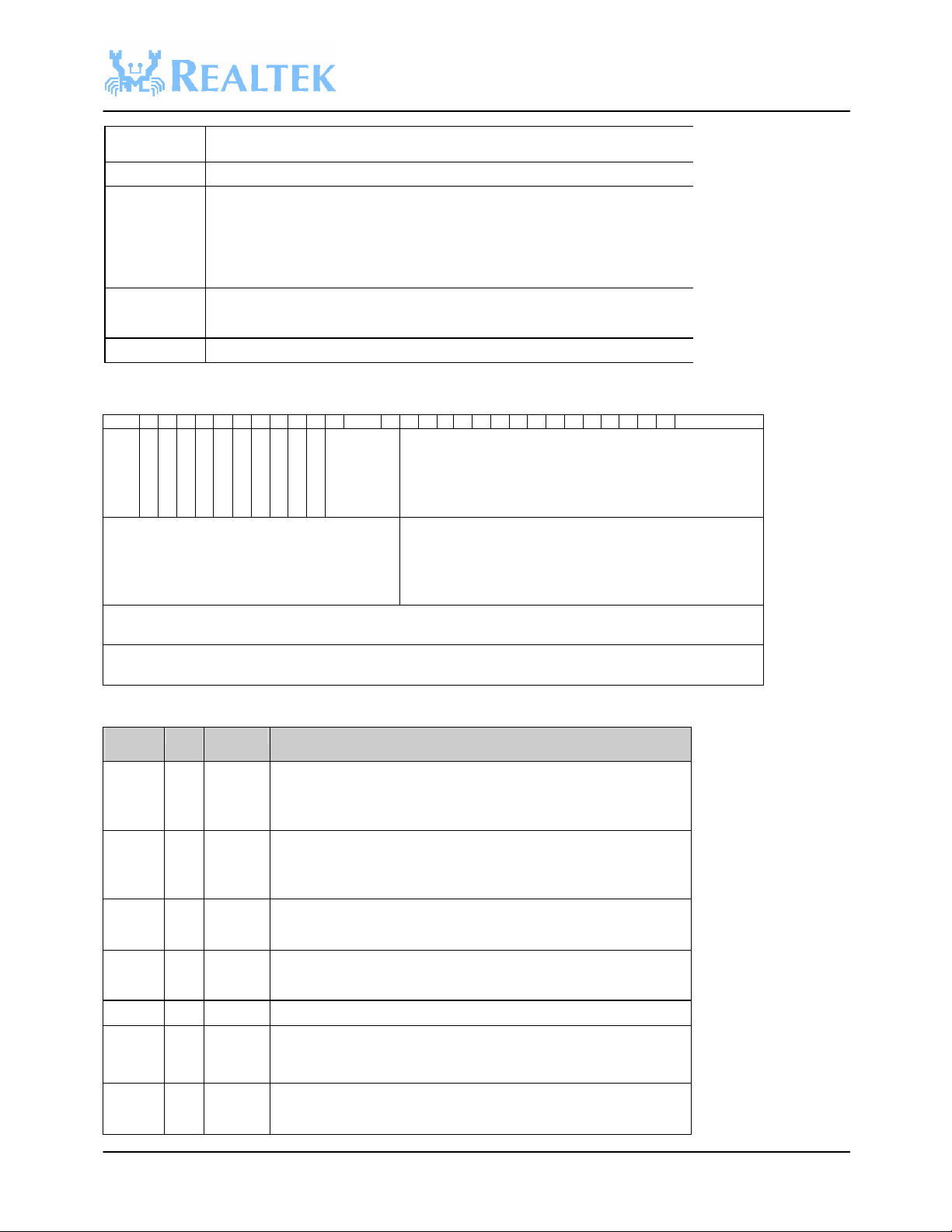
Tx Status Descriptor (after transmitting, OWN=0, Tx status mode) After having transmitted, the Tx descriptor turns to be a Tx
status descriptor.
31 30 29 28 27 26 25 24 23 22 21 20 19 18 17 16 15 14 13 12 11 10 9 8 7 6 5 4 3 2 1 0
O
FS LS R
W
N
=
0
R
U
E
E
N
S
S
F
V
V
R
T
E
E
S
S
V
RESV
Transmit frame length. This field indicates the length in TX buffer, in
byte, to be transmitted
00: Packet remains unchanged when transmitting
10: Add TAG. 0x8100 (Ethernet encoded tag protocol ID, indicating
that this is a IEEE 802.1Q VLAN packet) is inserted after source
address, and 2 bytes are inserted after tag protocol ID from
VLAN_TAG field in transmit descriptor.
The 2-byte VLAN_TAG contains information, from upper layer, of
user priority, canonical format indicator, and VLAN ID. Please refer to
IEEE 802.1Q for detailed VLAN tag information.
O
L
E
CC3-0
W
N
X
C
K
C
F
TAGC
Frame_Length
VLAN_TAG
Offset 0
Offset 4
TX_BUFFER_ADDRESS
Dummy
Offset 8
Offset 12
Byte
Offset#
0 31 OWN When set, indicates that the descriptor is owned by NIC. When clear
0 30 EOR End of descriptor Ring. When set, indicates that this is the last
0 29 FS First segment descriptor. When set, indicates that this is the first
0 28 LS Last segment descriptor. When set, indicates that this is the last
0 27-26 - Reserved.
0 25 UNF FIFO underrun. A status bit. NIC sets this bit to inform driver that
0 24 - Reserved.
0 23 TES Transmit Error Summary. When set, indicates that at least one of the
CONFIDENTIAL v1.0
Bit# Bit Name Description
indicates that the descriptor is owned by host system. NIC clears this
bit when the relative buffer data is already transmitted. In this case,
OWN=0.
descriptor in descriptor ring. When NIC’s internal transmit pointer
reaches here, the pointer will return to the first descriptor of the
descriptor ring after transmitting the data relative to this descriptor.
descriptor of a Tx packet, and this descriptor is pointing to the first
segment of the packet.
descriptor of a Tx packet, and this descriptor is pointing to the last
segment of the packet.
FIFO underrun had ever occurred before this packet transmitted.
following errors occurred: OWC, EXC, LNKF. This bit is valid only
when LS (Last segment bit) is set.
27
Page 28
RTL8181
0 22 OWC Out of Window Collision. A status bit. Out of window collision, When
set, it means an “out-of-window” collision is encountered during
transmitting packet.
0 21 LNKF Link Failure. A status bit. NIC sets this bit to inform link failure to
driver
0 20 EXC Excessive Collision. When set, indicates that the transmission was
aborted owing to consecutive 16 collisions.
0 19-16 CC3-0 Collision Counter. When Own bit =0, it’s a status field, A 4-bit
collision counter, shows the total collision times before the packet was
transmitted.
0 23-16 - Reserved.
0 15-0 Frame_Le
ngth
4 31-18 RSEV Reserved.
4 17-16 TAGC VLAN tag control bits:
4 15-0 VLAN_T
AG
8 31-0 TxBuff Logic Address of transmission buffer.
Transmit frame length. This field indicates the length in TX buffer, in
byte, to be transmitted
00: Packet remains unchanged when transmitting.
10: Add TAG. 0x8100 (Ethernet encoded tag protocol ID, indicating
that this is an IEEE 802.1Q VLAN packet) is inserted after source
address, and 2 bytes are inserted after tag protocol ID from
VLAN_TAG field in transmit descriptor.
The 2-byte VLAN_TAG contains information, from upper layer, of
user priority, canonical format indicator, and VLAN ID. Please refer to
IEEE 802.1Q for detailed VLAN tag information.
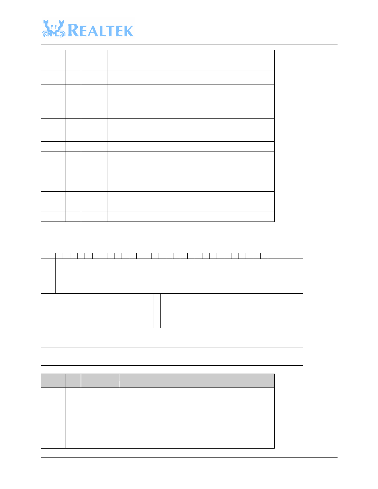
Reception Descriptor
Rx Command Descriptor (OWN=1)
31 30 29 28 27 26 25 24 23 22 21 20 19 18 17 16 15 14 13 12 11 10 9 8 7 6 5 4 3 2 1 0
O
W
N
=
1
RESV
RESV
RX_BUFFER_ADDRESS
T
A
V
A
Dummy
Buffer_Size
VLAN_TAG Offset 4
Offset 0
Offset 8
Offset 12
Bye
Offset#
0 31 OWN When set, indicates that the descriptor is owned by NIC, and is
0 30 EOR End of Rx descriptor Ring. Set to 1 indicates that this descriptor
Bit# Bit Name Description
ready to receive packet. The OWN bit is set by driver after
having pre-allocated buffer at initialization, or the host has
released the buffer to driver. In this case, OWN=1.
is the last descriptor of Rx descriptor ring. Once NIC’s internal
receive descriptor pointer reaches here, it will return to the first
descriptor of Rx descriptor ring after this descriptor is used by
packet reception.
CONFIDENTIAL v1.0
28
Page 29
RTL8181
0 29-13 - Reserved.
0 12-0 Buffer_Size This field indicate the receiver buffer size in bytes. Although the
maximum buffer size is 8K bytes/buffer, the NIC purges all data
after 4K bytes if the packet is larger than 4K-byte long.
4 31-17 RSEV Reserved.
4 16 TAVA Tag Available. When set, the received packet is an IEEE802.1Q
VLAN TAG (0x8100) available packet.
4 15-0 VLAN_TAG If the packet ‘s TAG is 0x8100, The
NIC extracts four bytes from after source ID, sets TAVA bit to1,
and moves the TAG value to this field in Rx descriptor.
8 31-0 RxBuff Logic Address of receive buffer.
Rx Status Descriptor (OWN=0)
31 30 29 28 27 26 25 24 23 22 21 20 19 18 17 16 15 14 13 12 11 10 9 8 7 6 5 4 3 2 1 0
O
FS LS F
W
N
=
0
M
P
B
B
F
R
R
R
C
P
P
U
T
A
A
A
A
O
O
W
E
U
R
I
I
IP
D
C
E
R
M
R
V
V
T
S
N
C
D
D
F
P
P
F
F
RESV
T
1
0
F
F
T
A
V
A
Frame_Length Offset 0
Offset 4
VLAN_TAG
RX_BUFFER_ADDRESS
Dummy
Bye
Offset#
0 31 OWN When set, indicates that the descriptor is owned by NIC. When
0 30 EOR End of Rx descriptor Ring. Set to 1 indicates that this descriptor is the
0 29 FS First segment descriptor. When set, indicates that this is the first
0 28 LS Last segment descriptor. When set, indicates that this is the last
0 27 FAE Frame Alignment Error. When set, indicates a frame alignment error
0 26 MAR Multicast Address packet Received: When set, indicates that a
0 25 PAM Physical Address Matched. When set, indicates that the destination
0 24 BAR Broadcast Address Received. When set, indicates that a broadcast
Bit# Bit Name Description
cleared, indicates that the descriptor is owned by host system. NIC
clears this bit when NIC has filled up this Rx buffer with a packet or
part of a packet. In this case, OWN=0.
last descriptor of Rx descriptor ring. Once NIC’s internal receive
descriptor pointer reaches here, it will return to the first descriptor of
Rx descriptor ring after this descriptor is used by packet reception.
descriptor of a received packet, and this descriptor is pointing to the
first segment of the packet.
descriptor of a received packet, and this descriptor is pointing to the
last segment of the packet.
has occurred on the received packet. The FAE packet is able to be
received only when RCR_AER is set.
multicast packet is received
address of this Rx packet matches to the value in NIC ’s ID registers.
packet is received. BAR and MAR will not be set simultaneously.
Offset 8
Offset 12
CONFIDENTIAL v1.0
29
Page 30

RTL8181
Receive Watchdog Timer expired. When set, indicates that the received
Tag Available. When set, the received packet is an IEEE802.1Q VLAN
0 23 BOVF Buffer Overflow. When set, indicates that receive buffer has ever
exhausted before this packet is received.
0 22 FOVF FIFO Overflow. When set, indicates that FIFO overflow has ever
occurred before this packet is received.
0 21 RWT
packet length exceeds 1724 bytes, the receive watchdog timer will
expire and stop receive engine.
0 20 RES Receive Error Summary. When set, indicates at least one of the
following errors occurred: CRC, RUNT, RWT, FAE. This bit is valid
only when LS(Last segment bit) is set
0 19 RUNT Runt packet. When set, indicates that the received packet length is
smaller than 64 bytes. RUNT packet is able to be received only when
RCR_AR is set.
0 18 CRC CRC error. When set, indicates that a CRC error has occurred on the
received packet. A CRC-error packet can be received only when
RCR_AER is set.
0 17-16 PDI[1:0] Protocol ID1, Protocol ID0
00: Non-IP
01: TCP/IP
10: UDP/IP
11: IP.
0 15 IPF When set, indicates IP checksum failure.
0 14 UDPF When set, indicates UDP checksum failure.
0 13 TCPF When set, indicates TCP checksum failure.
0 12-0 Frame_Le
ngth
4 31-17 RSEV Reserved.
4 16 TAVA
4 15-0 VLAN_T
AG
8 31-0 RxBuff Logic Address of receive buffer.
When OWN=0 and LS =1, it indicates the received packet length
including CRC, in bytes.
TAG (0x8100) available packet.
If the packet ‘s TAG is 0x8100, The NIC extracts four bytes from after
source ID, sets TAVA bit to1, and moves the TAG value to this field in
Rx descriptor.
9. UART Controller
RTL8181 provides a 16C550 compatible UART, which contains 16 byte FIFOs. In addition, auto flow control is provided, in
which, auto-CTS mode (CTS controls transmitter) and auto-RTS mode (Receiver FIFO contents and threshold control RTS)
are both supported. The baud rate is programmable and allows division of any input reference clock by 1 to (2^16-1) and
generates an internal 16x clock. RTL8181 provides fully programmable serial interface, which can be configured to support
7,8 bit characters, even, odd, no parity generation and detection, and 1 or 2 stop bit generation. Last, fully prioritized interrupt
control and loopback functionality for diagnostic capability are also provided.
The clock source is 22MHz.
UART Register Set
Virtual address Size (byte) Name Description Access
0xBD01_00C3 1 UART_RBR Receiver buffer register. (DLAB=0) R
0xBD01_00C3 1 UART_THR Transmitter holding register. (DLAB=0) W
0xBD01_00C3 1 UART_DLL Divisor latch LSB. (DLAB=1) R/W
0xBD01_00C7 1 UART_IER Interrupt enable register. (DLAB=0) R/W
0xBD01_00C7 1 UART_DLM Divisor latch MSB. (DLAB=1) R/W
0xBD01_00CB 1 UART_IIR Interrupt identification register. R
0xBD01_00CB 1 UART_FCR FIFO control register W
0xBD01_00CF 1 UART_LCR Line control register R/W
0xBD01_00D3 1 UART_MCR Modem control register R/W
CONFIDENTIAL v1.0
30
Page 31
RTL8181
0xBD01_00D7 1 UART_LSR Line status register R/W
0xBD01_00DB 1 UART_MSR Modem status register R/W
0xBD01_00DF 1 UART_SCR Scratch register R/W
Interrupt Enable Register (UART_IER)
Bit Bit Name Description R/W InitVal
7-6 - Reserved
5 ELP Low power mode enable R/W 0
3 EDSSI Enable modem status registe r interrupt R/W 0
4 ESLP Sleep mode enable R/W 0
2 ELSI Enable receiver line status interrupt R/W 0
1 ETBEI Enable transmitter holding register empty interrupt R/W 0
0 ERBI Enable received data available interrupt R/W 0
Interrupt Identification Register (UART_IIR)
Bit Bit Name Description R/W InitVal
7:5 FIFO64[2:0] 000 = no FIFO
110 = 16-byte FIFO
4 - Reserved R 0
R 110
3:1 IID[2:0] Interrupt ID. IID[1:0] indicates the interrupt
priority.
0 IPND Interrupt pending
0 = interrupt pending
R 000
R 0
Interrupt Priority
Interrupt
Identification Register
Bit3 Bit2 Bit1 Bit0
0 0 0 1 None None None None
0 1 1 0 1 Receiver line
0 1 0 0 2 Received data
1 1 0 0 2 Character
0 0 1 0 3 Transmitter
0 0 0 0 4 Modem status CTS#,DSR#,RI#,DCD# Reading MSR
Priority
level
Interrupt type Interrupt source Interrupt reset
method
status
available
time-out
indication
holding register
empty
Overrun, parity, framing
errors or break
DR bit is set. Read RBR.
No characters have been
removed from or input to
FIFO during the last character
times and at 1 character in it.
THRE bit set.
Read LSR
Read RBR
Reading IIR or write
THR
FIFO Control Register (UART_FCR)
Bit Bit Name Description R/W InitVal
7-6 RTRG[1:0] Receiver trigger level
Trigger level: 16-byte
00 = 01
01 = 04
10 = 08
11 = 14
3-5 - Reserved
2 TFRST Transmitter FIFO reset. Writes 1 to clear the
transmitter FIFO.
1 RFRST Receiver FIFO reset. Writes 1 to clear the receiver
FIFO.
0 EFIFO Enable FIFO. When this bit is set, enable the W 0
CONFIDENTIAL v1.0
31
W 11
W 0
W 0
Page 32

RTL8181
transmitter and receiver FIFOs. Changing this bit
clears the FIFOs.
Line Control Register (UART_LCR)
Bit Bit Name Description R/W InitVal
7 DLAB Divisor latch access bit. R/W 0
6 BRK Break control. Set this bit force TXD to the
spacing (low) state.(break) Clear this bit to disable
break condition.
5-4 EPS[1:0] Even parity select
00 = odd parity
01 = even parity
10 = mark parity
11 = space parity
3 PEN Parity enable R/W 0
2 STB Number of stop bits
0 = 1 bit
1 = 2 bits
1-0 WLS[1:0] Word length select
10 = 7 bits
11 = 8 bits
R/W 0
R/W 0
R/W 0
R/W 11
Modem Control Register (UART_MCR)
Bit Bit Name Description R/W InitVal
7-6 - Reserved
5 AFE Auto flow control enable R/W 0
4 LOOP Loopback R/W 0
2-3 - Reserved
1 RTS Request to send
0 = Set RTS# high
1 = Set RTS# low
0 - Reserved
R/W 0
Line Status Register (UART_LSR)
Bit Bit Name Description R/W InitVal
7 RFE Errors in receiver FIFO. At least one parity,
framing and break error in the FIFO.
6 TEMT Transmitter empty
Character mode: both THR and TSR are empty.
FIFO mode: both transmitter FIFO and TSR are
empty
5 THRE Transmitter holding register empty.
Character mode: THR is empty.
FIFO mode: transmitter FIFO is empty
4 BI Break interrupt indicator R 0
3 FE Framing error R 0
2 PE Parity error R 0
1 OE Overrun error. An overrun occurs when the
receiver FIFO is full and the next character is
completely received in the receiver shift register.
An OE is indicated. The character in the shift
register will be overwritten.
0 DR Data ready.
Character mode: data ready in RBR
FIFO mode: receiver FIFO is not empty.
R 0
R 0
R 0
R 0
R 0
Modem Status Register (UART_MSR)
Bit Bit Name Description R/W InitVal
CONFIDENTIAL v1.0
32
Page 33

RTL8181
7 DCD In loopback mode, returns the bit 2 of MCR.
In normal mode, returns 1.
6 RI In loopback mode, returns the bit 3 of MCR.
In normal mode, returns 0.
5 DSR In loopback mode, returns the bit 0 of MCR
In normal mode, returns 1.
4 CTS Clear to send.
0 = CTS# detected high
1 = CTS# detected low
3-1 - Reserved
0
?CTS
Delta clear to send. CTS# signal transits. R 0
R 1
R 0
R 1
R 0
10. Timer & Watchdog
There are four sets of hardware timer and one watchdog timer. Each timer can be configured as timer mode or counter mode.
No matter counter or timer mode, the time value will be counted down from initial value to zero, which value is subtracted by
one in every timer clock. When configured as timer mode, the source of timer clock could be configured to use base clock
directly, or based on the base clock divided by a configurable register value – CDBR, which way is called as Basic timer.
When the value is reaching to zero, the timer is stopped and an interrupt will be issued in counter mode. If configured as timer
mode, beside to issue an interrupt, the time value will be reset to its initial value, and then count down timer be operated
continuously, and an interrupt will be issued periodically whenever the count down value reaches to zero.
When watchdog timer is enabled, it will cause the system reset when time out occurred. The time out interval could be selected
from register, the time unit value is based on base clock divided by the base value, which is same used by timer.
Timer & Watchdog Register Set
Virtual address Size (byte) Name Description Access
0xBD01_0050 2 TCCNR Timer/Counter control register R/W
0xBD01_0054 1 TCIR Timer/Counter interrupt register R/W
0xBD01_0058 1 CBDR Clock division base register R/W
0xBD01_005C 2 WDTCNR Watchdog timer control register R/W
0xBD01_0060 3 TC0DATA Timer/Counter 0 data register. It specifies the
time-out duration.
0xBD01_0064 3 TC1DATA Timer/Counter 1 data register. It specifies the
time-out duration.
0xBD01_0068 4 TC2DATA Timer/Counter 2 data register. It specifies the
time-out duration.
0xBD01_006C 4 TC3DATA Timer/Counter 3 data register. It specifies the
time-out duration.
0xBD01_0070 3 TC0CNT Timer/Counter 0 count register R
0xBD01_0074 3 TC1CNT Timer/Counter 1 count register R
0xBD01_0078 4 TC2CNT Timer/Counter 2 count register R
0xBD01_007C 4 TC3CNT Timer/Counter 3 count register R
Timer/Counter 0 Data register (TC0CNT)
Bit Bit Name Description R/W InitVal
23-0 TC0Value[23:0] The timer or counter initial value R/W
Timer/Counter 1 Data register (TC1CNT)
Bit Bit Name Description R/W InitVal
23-0 TC1Value[23:0] The timer or counter initial value R/W
Timer/Counter 2 Data register (TC2CNT)
Bit Bit Name Description R/W InitVal
31-0 TC2Value[31:0] The timer or counter initial value R/W
R/W
R/W
R/W
R/W
CONFIDENTIAL v1.0
33
Page 34

RTL8181
Timer/Counter 3 Data register (TC3CNT)
Bit Bit Name Description R/W InitVal
31-0 TC3Value[31:0] The timer or counter initial value R/W
Timer/Counter Control register (TCCNR)
Bit Bit Name Description R/W InitVal
11 TC3Src Timer/Counter 3 clock source
0=Base clock
1=Basic timer
10 TC2Src Timer/Counter 2 clock source
0=Base clock
1=Basic timer
9 TC1Src Timer/Counter 1 clock source
0=Base clock
1=Basic timer
8 TC0Src Timer/Counter 0 clock source
0=Base clock
1=Basic timer
7 TC3Mode Timer/Counter 3 mode
0=counter mode
1=timer mode
6 TC3En Timer/Counter 3 enable R/W 0
5 TC2Mode Timer/Counter 2 mode
0=counter mode
1=timer mode
4 TC2En Timer/Counter 2 enable R/W 0
3 TC1Mode Timer/Counter 1 mode
0=counter mode
1=timer mode
2 TC1En Timer/Counter 1 enable R/W 0
1 TC0Mode Timer/Counter 0 mode
0=counter mode
1=timer mode
0 TC0En Timer/Counter 0 enable R/W 0
R/W 0
R/W 0
R/W 0
R/W 0
R/W 0
R/W 0
R/W 0
R/W 0
Timer/Counter Interrupt Register (TCIR)
Bit Bit Name Description R/W InitVal
7 TC3IP Timer/Counter 3 interrupt pending. Write “1” to
clear the interrupt.
6 TC2IP Timer/Counter 2 interrupt pending. Write “1” to
clear the interrupt.
5 TC1IP Timer/Counter 1 interrupt pending. Write “1” to
clear the interrupt.
4 TC0IP Timer/Counter 0 interrupt pending. Write “1” to
clear the interrupt.
3 TC3IE Timer/Counter 3 interrupt enable R/W 0
2 TC2IE Timer/Counter 2 interrupt enable R/W 0
1 TC1IE Timer/Counter 1 interrupt enable R/W 0
0 TC0IE Timer/Counter 0 interrupt enable R/W 0
R/W 0
R/W 0
R/W 0
R/W 0
Clock Division Base Register (CDBR)
Bit Bit Name Description R/W InitVal
15-0 DivFactor The divided factor of clock source. If DivFactor is
N, the watchdag timer divide by N+1.This value
could not be 0 in timer mode or watchdog. The
clock source is 22MHz.
R/W 0
Watchdog Control Register (WDTCNR)
CONFIDENTIAL v1.0
34
Page 35
RTL8181
Watchdog enable. When these bits are set to 0xA5,
Bit Bit Name Description R/W InitVal
10-9 OVSEL[1:0] Overflow select. These bits specify the overflow
condition when the watchdog timer counts to the
value.
00 = 213
01 = 214
10 = 215
11 = 216
8 WDTCLR Watchdog clear. Write a 1 to clear the watchdog
counter. It is auto cleared after the write.
7-0 WDTE[7:0]
the watchdog timer stops. Other value can enable
the watchdog timer and cause a system reset when
an overflow signal occurs.
R/W 00
W 0
W 0xA5
11. GPIO Control
RTL8181 provides two sets of GPIO pins – PortA and PortB . PortA has 16 pins and PortB has 16 pins. Every GPIO pin can
be configured as input or output pins via register PA(B)DIR. Register PA(B)DATA could be used to control the signals (high
or low) of GPIO pins. Because the GPIO pins might be shared with some peripheral pins, the PA(B)CNR can control the
attribute of the shared pins. Besides, PortB GPIO sets can be used to generate interrupt via PBIMR, and the interrupt status is
shown in PBISR.
GPIO Register Set
Virtual address Size (byte) Name Description Access
0xBD01_0040 4 PABDIR Port A/B direction register R/W
0xBD01_0044 4 PABDATA Port A/B data register R/W
0xBD01_0048 4 PBIMR Port B interrupt mask register R/W
0xBD01_004C 4 PBISR Port B interrupt register R
Port A,B Direction Register (PADIR , PBDIR)
Bit Bit Name Description R/W InitVal
31-16 DRCA[15:0] Pin direction configuration of Port A
0 = configured as input pin
1 = configured as output pin
15-0 DRCB[15:0] Pin direction configuration of Port B
0 = configured as input pin
1 = configured as output pin
Port A,B DATA Register (PADATA, PBDATA)
Bit Bit Name Description R/W InitVal
31-16 DATAA[15 :0] Pin data of Port A R/W 00
15-0 DATAB [15:0] Pin data of Port B R/W 00
R/W 00
R/W 00
Port B Interrupt Mask Register (PBIMR)
Bit Bit Name Description R/W InitVal
1-0 PB0IM[1:0] PortB.0 interrupt mode
00 = disable interrupt
01 = enable falling edge interrupt
10 = enable rising edge interrupt
11 = enable both falling or rising edge interrupt
3-2 PB1IM[1:0] PortB.1 interrupt mode
00 = disable interrupt
01 = enable falling edge interrupt
CONFIDENTIAL v1.0
35
R/W 00
R/W 00
Page 36

RTL8181
10 = enable rising edge interrupt
11 = enable both falling or rising edge interrupt
5-4 PB2IM[1:0] PortB.2 interrupt mode
00 = disable interrupt
01 = enable falling edge interrupt
10 = enable rising edge interrupt
11 = enable both falling or rising edge interrupt
7-6 PB3IM[1:0] PortB.3 interrupt mode
00 = disable interrupt
01 = enable falling edge interrupt
10 = enable rising edge interrupt
11 = enable both falling or rising edge interrupt
9-8 PB4IM[1:0] PortB.4 interrupt mode
00 = disable interrupt
01 = enable falling edge interrupt
10 = enable rising edge interrupt
11 = enable both falling or rising edge interrupt
11-10 PB5IM[1:0] PortB.5 interrupt mode
00 = disable interrupt
01 = enable falling edge interrupt
10 = enable rising edge interrupt
11 = enable both falling or rising edge interrupt
13:12 PB6IM[1:0] PortB.6 interrupt mode
00 = disable interrupt
01 = enable falling edge interrupt
10 = enable rising edge interrupt
11 = enable both falling or rising edge interrupt
15-14 PB7IM[1:0] PortB.7 interrupt mode
00 = disable interrupt
01 = enable falling edge interrupt
10 = enable rising edge interrupt
11 = enable both falling or rising edge interrup t
17-16 PB8IM[1:0] PortB.8 interrupt mode
00 = disable interrupt
01 = enable falling edge interrupt
10 = enable rising edge interrupt
11 = enable both falling or rising edge interrupt
19-18 PB9IM[1:0] PortB.9 interrupt mode
00 = disable interrupt
01 = enable falling edge interrupt
10 = enable rising edge interrupt
11 = enable both falling or rising edge interrupt
21-20 PB10IM[1:0] PortB.10 interrupt mode
00 = disable interrupt
01 = enable falling edge interrupt
10 = enable rising edge interrupt
11 = enable both falling or rising edge interrupt
23:22 PB11 IM[1:0] PortB.11 interrupt mode
00 = disable interrupt
01 = enable falling edge interrupt
10 = enable rising edge interrupt
11 = enable both falling or rising edge interrupt
25-24 PB12IM[1:0] PortB.12 interrupt mode
00 = disable interrupt
01 = enable falling edge interrupt
10 = enable rising edge interrupt
11 = enable both falling or rising edge interrupt
27-26 PB13IM[1:0] PortB.13 interrupt mode
00 = disable interrupt
R/W 00
R/W 00
R/W 00
R/W 00
R/W 00
R/W 00
R/W 00
R/W 00
R/W 00
R/W 00
R/W 00
R/W 00
CONFIDENTIAL v1.0
36
Page 37

RTL8181
01 = enable falling edge interrupt
10 = enable rising edge interrupt
11 = enable both falling or rising edge interrupt
29-28 PB14IM[1:0] PortB.14 interrupt mode
R/W 00
00 = disable interrupt
01 = enable falling edge interrupt
10 = enable rising edge interrupt
11 = enable both falling or rising edge interrupt
31-30 PB15IM[1:0] PortB.15 interrupt mode
R/W 00
00 = disable interrupt
01 = enable falling edge interrupt
10 = enable rising edge interrupt
11 = enable both falling or rising edge interrupt
Port B Interrupt Status Register (PBISR)
Bit Bit Name Description R/W InitVal
15-0 PBIP[15:0] Interrupt pending status. Self clear after read. R 00
12. 802.11b WLAN Controller
RTL8181 integrates with a wireless LAN MAC and a direct sequence spread spectrum baseband processor, and is full
compliance with IEEE 802.11 and IEEE 802.11b specifications.
RTL8181 has on board A/D and D/A converters for analog I and Q inputs and outputs. Differential phase shift keying
modulation schemes DBPSK and DQPSK, with data scrambling capability, are available along with complementary code
keying to provide a variety of data rates. Both receive and transmit AGC functions obtain maximum performance in the analog
portions of the transceiver. It also includes a built-in enhanced signal detector to alleviate severe multi-path effects. The target
environment for 11Mbps is 125ns RMS delay spread. It also supports short preamble and antenna diversity. For security issues,
RTL8181 has implemented a high performance internal WEP engine supporting up to 104-bits WEP.
The WLAN controller is a DMA bus-master device, and uses descriptor-based buffer structure for packet transmission and
reception. These features will definitely offload much CPU loading.
RTL818 provides various interfaces for external RF module. Currently, it could interface with the RF modules as Intersil,
RFMD and Philip.
WLAN Controller register Set
Virtual Address Size
0xBD40_0000 8 WLAN_ID ID Register : The ID register is only permitted to write by 4-byte
0xBD40_0008 8 WLAN_MAR Multicast Register: The MAR register is only permitted to write by
0xBD40_0018 8 WLAN_TSFTR Timing Synchronization Function Timer Register R
0xBD40_0020 4 WLAN_TLPDA Transmit Low Priority Descriptors Start Address (32-bit).
0xBD40_0024 4 WLAN_TNPDA Transmit Normal Priority Descriptors Start Address (32-bit).
0xBD40_0028 4 WLAN_THPDA Transmit High Priority Descriptors Start Address (32-bit).
0xBD40_002C 4 WLAN_BRSR Basic Rate Set Register R/W
0xBD40_002E 6 WLAN_BSSID Basic Service Set ID R/W
0xBD40_0037 1 WLAN_CR Command Register R/W
0xBD40_003C 2 WLAN_IMR Interrupt Mask Register R/W
0xBD40_003E 2 WLAN_ISR Interrupt Status Register R/W
0xBD40_0040 4 WLAN_TCR Transmit (Tx) Configuration Register R/W
0xBD40_0044 4 WLAN_RCR Receive (Rx) Configuration Register R/W
0xBD40_0048 4 WLAN_TINT Timer Interrupt Register. Once having written a nonzero value to R/W
Name Description R/W
(byte)
R/W
access. Read access can be byte, word, or double word access.
R/W
4-bye access. Read access can be byte, word, or double word
access.
R/W
(256-byte alignment)
R/W
(256-byte alignment)
R/W
(256-byte alignment)
CONFIDENTIAL v1.0
37
Page 38
RTL8181
this register, the Timeout bit of WLAN_ISR register will be set
whenever the least 32 bits of the WLAN_TSFTR reaches to this
value. The Timeout bit will never be set as long as WLAN_TINT
register is zero.
0xBD40_004C 4 WLAN_TBDA Transmit Beacon Descriptor Start Address (32-bit) (256-byte alignment) R/W
0xBD40_0050 1 WLAN_CR Command Register R/W
0xBD40_0051 1 WLAN_CONFIG0 Configuration Regist er 0 R
0xBD40_0053 1 WLAN_CONFIG2 Configuration Register 2 R/W
0xBD40_0054 4 WLAN_ANAPARM Analog parameter R/W
0xBD40_0058 1 WLAN_MSR Media Status Register R/W
0xBD40_0059 1 WLAN_CONFIG3 Configuration Register 3 R/W
0xBD40_005A 1 WLAN_CONFIG4 Configuration Register 4 R/W
0xBD40_005B 1 WLAN_TESTR TEST mode Register R/W
0xBD40_005F 1 WLAN_SCR Security Configuration Register R/W
0xBD40_0070 2 WLAN_BCNITV Beacon Interval Register R/W
0xBD40_0072 2 WLAN_ATIMWND Atim Window Register R/W
0xBD40_0074 2 WLAN_BINTRITV Beacon interrupt Interval Register R/W
0xBD40_0078 1 WLAN_PHYDELAY Phy Delay Register R/W
0xBD40_007A 2 WLAN_CRC16ERR PLCP header CRC16 error count R/W
0xBD40_007C 1 WLAN_PHYADDR Address register for Phy interface R/W
0xBD40_007D 1 WLAN_PHYDATAW Write Data to Phy W
0xBD40_007E 1 WLAN_PHYDATAR Read Data from Phy R
0xBD40_0080 4 WLAN_PHYCFG Phy Configuration Register R/W
0xBD40_0090 16 WLAN_DK0 WEP Default Key 0 Register R/W
0xBD40_00A0 16 WLAN_DK1 WEP Default Key 1 Register R/W
0xBD40_00B0 16 WLAN_DK2 WEP Default Key 2 Register R/W
0xBD40_00C0 16 WLAN_DK3 WEP Default Key 3 Register R/W
0xBD40_00D8 1 WLAN_ CONFIG5 Configuration Register 5 R/W
0xBD40_00D9 1 WLAN_TPPOLL Transmit Priority Polling Register W
0xBD40_00DC 2 WLAN_ CWR Contention Window Register R
0xBD40_00DE 1 WLAN_RETRYCTR Retry Count Register R
0xBD40_00E4 4 WLAN_RDSAR Receive Descriptor Start Address Register (32-bit) (256-byte
alignment)
0xBD40_0100 6 WLAN_KMAR Key Map MAC Address R/W
0xBD40_0106 15 WLAN_KMKEY Key Map Key Value R/W
0xBD40_0116 2 WLAN_KMC Key Map Config R/W
R/W
TSF timer register (WLAN_TSFTR)
Bit Bit Name Description R/W
63-0 TSFT Timing Synchronization Function Timer: RTL8181 maintain a TSF timer with modules 2^64
R
counting in increments of microseconds. The 8 octets are the timestamp field of beacon and
probe response frame.
Basic Rate Set Register (WLAN_BRSR)
Bit Bit Name Description
15-9 - Reserved
8 BPLCP 0:Long PLCP header for CTS/ACK packet.
1:Short PLCP header for CTS/ACK packet.
7-4 - Reserved
3-0 MBR Maximum Basic Service Set Basic Rate. All control frames shall be
transmitted at the rate that is less than or equal.
bit0: 1M, bit1: 2M, bit2: 5.5M, bit3: 11M.
Basic Service Set ID register (WLAN_BSSID)
Bit Bit Name Description R/W
47-0 BSSID Basic Service Set Identification: This register is written to by the driver after a NIC joins a
R/W
network or creates an adhoc network.
Command Register (WLAN_CR)
This register is used for issuing commands to WLAN controller. These commands are issued by setting the corresponding bits for
the function. A global software reset along with individual reset and enable/disable for transmitter and receiver are provided here.
CONFIDENTIAL v1.0
38
Page 39

RTL8181
Bit Bit Name Description R/W
7:5 - Reserved
4 RST Reset: Setting this bit to 1 forces the RTL8181 do the WLAN MAC reset. During reset
reset state, it will disable the transmitter and receiver, and reinitializes the FIFOs. The
values of WLAN_IDR and WLAN_MAR7 will have no changes. This bit is 1 during the
reset operation, and is cleared to 0 when the reset operation is complete.
3 RE Receiver Enable: When set to 1, and the receive state machine is idle, the receive machine
becomes active. This bit will read back as 1 whenever the receive state machine is active.
After initial power-up, software must insure that the receiver has completely reset before
setting this bit.
1: Enable
0: Disable
2 TE Transmitter Enable: When set to 1, and the transmit state machine is idle, the transmit state
machine becomes active. This bit will read back as 1 whenever the transmit state machine
is active. After initial power-up, software must insure that the transmitter has completely
reset before setting this bit.
1: Enable
0: Disable
1-0 - Reserved
R/W
R/W
R/W
Interrupt Mask Register (WLAN_IMR)
This register masks the interrupts that can be generated from the Interrupt Status Register. A hardware reset will clear all mask
bits. Setting a mask bit allows the corresponding bit in the Interrupt Status Register to cause an interrupt. The Interrupt Status
Register bits are always set to 1 if the condition is present, regardless of the state of the corresponding mask bit.
Bit Bit Name Description R/W
15 TXFOVW Tx FIFO Overflow Interrupt:
1: Enable
0: Disable
14 TimeOut Time Out Interrupt:
1: Enable
0: Disable
13 BcnInt Beacon Time out Interrupt:
1: Enable
0: Disable
12 ATIMInt ATIM Time Out Interrupt:
1: Enable
0: Disable
11 TBDER Tx Beacon Descriptor Error Interrupt:
1: Enable
0: Disable
10 TBDOK Tx Beacon Descriptor OK Interrupt:
1: Enable
0: Disable
9 THPDER Tx High Priority Descriptor Error Interrupt:
1: Enable
0: Disable
8 THPDOK Tx High Priority Descriptor OK Interrupt:
1: Enable
0: Disable
7 TNPDER Tx Normal Priority Descriptor Error Interrupt:
1: Enable
0: Disable
6 TNPDOK Tx Normal Priority Descriptor OK Interrupt:
1: Enable
0: Disable
5 RXFOVW Rx FIFO Overflow Interrupt:
1: Enable
0: Disable
4 RDU Rx Descriptor Unavailable Interrupt: R/W
CONFIDENTIAL v1.0
39
R/W
R/W
R/W
R/W
R/W
R/W
R/W
R/W
R/W
R/W
R/W
Page 40

RTL8181
Transmit Beacon Priority Descriptor Error: Indicates that a packet of beacon priority descriptor
(Short Retry Limit), and an SLRC (Station Long Retry Count) has reached LRL (Long Retry
(Short Retry Limit), and an SLRC (Station Long Retry Count) has reached LRL (Long Retry
1: Enable
0: Disable
3 TLPDER Tx Low Priority Descriptor Error Interrupt:
1: Enable
0: Disable
2 TLPDOK Tx Low Priority Descriptor OK Interrupt:
1: Enable
0: Disable
1 RER Rx Error Interrupt:
1: Enable
0: Disable
0 ROK Rx OK Interrupt:
1: Enable
0: Disable
R/W
R/W
R/W
R/W
Interrupt Status Register (WLAN_ISR)
This register indicates the source of WLAN controller interrupt goes active. Enabling the corresponding bits in the Interrupt
Mask Register (WLAN_IMR) allows bits in this register to produce an interrupt. When an interrupt is active, one of more bits
in this register are set to a “1”. The interrupt Status Register reflects all current pending interrupts, regardless of the state of the
corresponding mask bit in the WLAN_IMR. Reading the WLAN_ISR clears all interrupts. Writing a 1 to any bit in this
register will reset that bit.
Bit Symbol Description R/W
15 TXFOVW Tx FIFO Overflow R/W
14 TimeOut Time Out: This bit is set to 1 when the least 32 bits of the TSFTR register reaches to the
value of the TimerInt register.
13 BcnInt Beacon Time Out Interrupt: When set, this bit indicates that the TBTT (Target Beacon
Transmission Time) has been reached after the value of the Beacon interrupt Interval
register.
12 ATIMInt ATIM Time Out Interrupt: When set, this bit indicates that the ATIM window has been gone
after the value of the Beacon interrupt Interval register.
11 TBDER
transmission was aborted due to an Rx beacon frame.
10 TBDOK Transmit Be acon Priority Descriptor OK: Indicates that a packet of beacon priority
descriptor exchange sequence has been successfully completed.
9 THPDER Transmit High Priority Descriptor Error: Indicates that a packet of high priority descriptor
transmission was aborted due to an SSRC (Station Short Retry Count) has reached SRL
R/W
R/W
R/W
R/W
R/W
R/W
Limit).
8 THPDOK Transmit High Priority Descriptor OK: Indicates that a packet of high priority descriptor
exchange sequence has been successfully completed.
7 TNPDER Transmit Normal Priority Descriptor Error: Indicates that a packet of normal priority
descriptor transmission was aborted due to an SSRC (Station Short Retry Count) has
reached SRL (Short Retry Limit), and an SLRC (Station Long Retry Count) has reached
LRL (Long Retry Limit).
6 TNPDOK Transmit Normal Priority Descriptor OK: Indicates that a packet of normal priority
descriptor exchange sequence has been successfully completed.
5 FOVW Rx FIFO Overflow: This bit set to 1 is caused by RDU, poor PCI performance, or
overloaded PCI traffic.
4 _RDU Rx Descriptor Unavailable: When set, this bit indicates that the Rx descriptor is currently
unavailable.
3 TLPDER Transmit Low Priority Descriptor Error: Indicates that a packet of low priority descriptor
transmission was aborted due to an SSRC (Station Short Retry Count) has reached SRL
Limit).
2 TLPDOK Transmit Low Priority Descriptor OK: Indicates that a packet of low priority descriptor
exchange sequence has been successfully completed.
1 RER Receive Error: Indicates that a packet has a CRC32 or ICV error. R/W
0 ROK Receive OK: In normal mode, indicates the successful completion of a packet reception. R/W
CONFIDENTIAL v1.0
40
R/W
R/W
R/W
R/W
R/W
R/W
R/W
Page 41

RTL8181
MXDMA2, 1,
Append ICV: This bit indicates the existence of ICV appended at the end of an encipherment
Transmit Configuration Register (WLAN_TCR)
This register defines the Transmit Configuration for the WLAN controller. It controls such functions as loopback, heartbeat,
auto transmit padding, programmable inter- frame gap, fill and drain thresholds, and maximum DMA burst size.
Bit Symbol Description R/W
31 CWMIN Contention Window minimum value: Set to 1 to indicate that Cwmin=8. Set to 0 to indicate
that Cwmin=32.
30 SEQ GEN Sequence number generation switch.
0 – Enabled. Sequence number is generated by RTL8181.
1 – Disabled. Sequence number should be filled by software.
29-25 - Reserved
24 SAT Set ACK Timeout: The EIFS, ACK and CTS timeouts are derived from the following
equation:
EIFS = 112/ACKrate + 252
1: ACKrate is dependent on the maximum of MBR (bits 1:0, BRSR) and Rx DATA/RTS
rate.
0: ACKrate is fixed at 1Mbps.
23-21
0
20 DISCW Disable Contention Window Backoff: This bit indicates the existence of a backoff procedure
19 ICV
18-17 LBK1, LBK0 Loopback Test: There will be no packet on the TXI+/- and TXQ+/- lines under the
16 CRC Append CRC32: This bit indicates the existence of a CRC32 appended at the end of a
15-8 SRL RTS Retry Limit: Indicates the maximum retry times of RTS frame, data or management
7-0 LRL Data Packet Retry Limit: Indicates the maximum retransmission times of Data or
Max DMA Burst Size per Tx DMA Burst: This field sets the maximum size of transmit
DMA data bursts according to the following table:
000: 16 bytes
001: 32 bytes
010: 64 bytes
011: 128 bytes
100: 256 bytes
101: 512 bytes
110: 1024 bytes
111: 2048 bytes
during packet transmission.
1: No random backoff procedure
0: Uses IEEE 802.11 random backoff procedure
packet.
1: No ICV appended
0: ICV appended
Loopback test condition. The loopback function must be independent of the link state.
00: Normal operation
01: MAC Loopback
10: Baseband Loopback
11: Continue TX.
packet.
1: No CRC32 appended
0: A CRC32 is appended
frame of length less than or equal to RTSThreshold.
Management frame of length greater than RTSThreshold.
R/W
R/W
R/W
R/W
R/W
R/W
R/W
R/W
R/W
Receive Configuration Register (WLAN_RCR)
This register is used to set the receive configuration for the WLAN controller. Receive properties such as accepting error
packets, runt packets, setting the receive drain threshold etc. are controlled here.
Bit Bit Name Description R/W
31 ONLYERLP
KT
30 ENCS2 Enable Carrier Sense Detection Method 2 R/W
CONFIDENTIAL v1.0
Early Receiving based on Packet Size: Early Receiving is only performed for packets with a
size greater than 1536 bytes.
41
R/W
Page 42

RTL8181
MXDMA2, 1,
29 ENCS1 Enable Carrier Sense Detection Method 1 R/W
28 ENMARP Enable MAC Autoreset PHY R/W
27-24 - Reserved R/W
23 CBSSID Check BSSID, To DS, From DS Match Packet: When set to 1, the RTL8181 will check the
Rx data type frame’s BSSID, To DS and From DS fields, according to NETYPE (bits 3:2,
MSR), to determine if it is set to Link ok at an Infrastructure or Adhoc network.
22 APWRMGT Accept Power Management Packet: This bit will determine whether the RTL8181 will
accept or reject packets with the power management bit set.
1: Accept
0: Reject
21 ADD3 Accept Address 3 Match Packets: Set this bit to 1 to accept broadcast/multicast data type
frames that Address 3 matching RTL8181’s MAC address. This bit is valid only when
NETYPE (bits 3:2, MSR) is set to Link ok in an Infrastructure network.
20 AMF Accept Management Frame: This bit will determine whether the RTL8181 will accept or
reject a management frame.
1: Accept
0: Reject
19 ACF Accept Control Frame: This bit will determine whether the RTL8181 will accept or reject a
control frame.
1: Accept
0: Reject
18 ADF Accept Data Frame: This bit will determine whether the RTL8181 will accept or reject a
data frame.
1: Accept
0: Reject
17-16 - Reserved
15-13 RXFTH2, 1, 0 Rx FIFO Threshold: This bit specifies the Rx FIFO Threshold level. When the number of
the received data bytes from a packet, which is being received into the Rx FIFO of the
RTL8181, has reached to this level (or the FIFO has contained a complete packet), the
receive PCI bus master function will begin to transfer the data from the FIFO to the ho st
memory. This field sets the threshold level according to the following table:
000: Reserved
001: Reserved
010: 64 bytes
011: 128 bytes
100: 256 bytes
101: 512 bytes
110: 1024 bytes
111: No Rx threshold. The RTL8181 begins the transfer of data after having received a
whole packet into the FIFO.
12 AICV Accept ICV Error Packet: This bit determines whether all packets with ICV error will be
accepted or rejected.
1: Accept
0: Reject
11 - Reserved
10-8
0
7-6 - Reserved
5 ACRC32 Accept CRC32 Error Packet: When set to 1, all packets with CRC32 error will be accepted.
CONFIDENTIAL v1.0
Max DMA Burst Size per Rx DMA Burst: This field sets the maximum size of the receive
DMA data bursts according to the following table:
000: 16 bytes
001: 32 bytes
010: 64 bytes
011: 128 bytes
100: 256 bytes
101: 512 bytes
110: 1024 bytes
111: Unlimited
When set to 0, all packets with CRC32 error will be rejected.
1: Accept
42
R/W
R/W
R/W
R/W
R/W
R/W
Page 43

RTL8181
0: Reject
4 - Reserved
3 AB Accept Broadcast Packets: This bit determines whether broadcast packets will be accepted
or rejected.
1: Accept
0: Reject
2 AM Accept Multicast Packets: This bit determines whether multicast packets will be accepted or
rejected.
1: Accept
0: Reject
1 APM Accept Physical Match Packets: This bit determines whether physical match packets will be
accepted or rejected.
1: Accept
0: Reject
0 AAP Accept Destination Address Packets: This bit determines whether all packets with a
destination address will be accepted or rejected.
1: Accept
0: Reject
Command Register (WLAN_CR)
This register is used for issuing commands to the WLAN controller. These commands are issued by setting the corresponding bits
for the function. A warm software reset along with individual reset and enable/disable for transmitter and receiver are provided as
well.
Bit Bit Name Description R/W
7-6 EEM These 2 bits select the operating mode.
00: Operating in network/host communication mode.
11: Before writing to the WLAN_CONFIG0, 1, 2, and 3 registers, the RTL8181 must be
placed in this mode. This will prevent accidental change of the configurations of the WLAN
controller.
5-0 - Reserved
R/W
Configuration Register 0 (WLAN_CONFIG0)
Bit Bit Name Description R/W
7-4 - Reserved
3 Aux_Status Auxiliary Power Present Status: This bit indicates the existence of Aux. power. The value of
this bit is fixed after each reset.
1: Aux. Power is present
0: Aux. Power is absent
2 - Reserved
1-0 GL Geographic Location: These bits indicate the current operational region in which RTL818 1
transmits and receives packets..
USA: 11, Europe: 10, Japan: 0
R/W
R/W
Configuration Register 2 (WLAN_CONFIG2)
Bit Bit Name Description R/W
7 LCK Locked Clocks: Set this bit to 1 to indicate that the transmit frequency and symbol clocks are
derived from the same oscillator.
6 ANT Antenna Diversity:
1: Enable
0: Disable
5-4 - Reserved 3 DPS Descriptor Polling State: Test mode..
0: Normal working state. This is also the power-on default value.
1: Test Mode
2 PAPE_sign 1: RTL8181 will advance PAPE_time to enable the PAPE pin when Tx data
0: RTL8181 will delay PAPE_time to enable the PAPE pin when Tx data
1-0 PAPE_time These two bits indicate that the RTL8181 has enabled the PAPE pin in µs. R/W
CONFIDENTIAL v1.0
43
R/W
R/W
R/W
R/W
Page 44

RTL8181
Media Status Register (WLAN_MSR)
This register allows configuration of device and PHY options, and provides PHY status information.
Bit Bit Name Description R/W
7-4 - Reserved 3-2 NETTYPE Network Type and Link Status: The values of these bits are written by the driver.
10: Infrastructure client, 01: Ad hoc, 11: Access Point, 00: No link
1-0 - Reserved -
R/W
Configuration Register 3 (WLAN_CONFIG3)
Bit Bit Name Description R/W
7 - Reserved
6 PARM_En Parameter Write Enable:
Setting this bit to 1 and the WLAN_CR register EEM1=EEM0=1 enables the
WLAN_ANAPARM register to be written via software.
4-1 -- Reserved 0 FBtBEn Fast Back to Back Enable:
1: Enable
0: Disable
Configuration Register 4 (WLAN_CONFIG4)
Bit Bit Name Description R/W
7 VCOPDN VCO Power Down:
1: VCO Power Down mode. Setting this bit will enable VCOPDN pin and turn
off the external RF front end power (including VCO) and most of the internal
power of the RTL8181.
0: Normal working state. This is the power-on default value.
6 PWROFF Power Off:
1: Power Off mode. Turn off the external RF front end power (excluding VCO)
and most of the internal power of the RTL8181.
0: Normal working state. This is the power-on default value.
5 PWRMGT Power Management:
1: Power Management mode. Set Tx packet’s power management bit to 1 include
control type frame.
0: Normal working state. This is the power-on default value.
4-2 - Reserved 1-0 RFTYPE Radio Front End Programming Method: The combination of these two bits
indicate what kind of the RF module is being used with the RTL8181.
11: Philips, 10: RFMD, 01: Intersil
R/W
R/W
R/W
R/W
R/W
R/W
Security Configuration Register (WLAN_SCR)
Bit Bit Name Description R/W
7-6 - Reserved 5-4 KM Key Mode: The combination of these two bits indicate what kind of security
scheme is being used.
01: WEP40, 01: WEP104
3-2 - Reserved 1 TXSECON TX Security ON:
Set this bit to 1 to turn on the option security scheme of the Tx path. This bit is
written by software and is invalid when WEP40 (bit 7, WLAN_CONFIG0), and
WEP104 (bit 6, WLAN_CONFIG0) are set to 0.
0 RXSECON RX Security ON:
Set this bit to 1 to turn on the option security scheme of the Rx path. This bit is
written by software and is invalid when WEP40 (bit 7, WLAN_CONFIG0), and
WEP104 (bit 6, WLAN_CONFIG0) are set to 0.
R/W
R/W
R/W
CONFIDENTIAL v1.0
44
Page 45
RTL8181
egister will generate BcnInt (bit 13, ISR) at a setting time interval before TBTT to
Beacon Interval Register (WLAN_BCNITV)
Bit Bit Name Description R/W
15-10 - Reserved 9-0 BcnItv Beacon Interval: The Beacon Interval represents the number of time units (1 TU =
1024µs) between target beacon transmission times (TBTTs). This register is
written by the driver after starting a BSS/IBSS or joining IBSS network.
ATIM Window Register (WLAN_ATIMWND)
Bit Bit Name Description R/W
15-10 -- Reserved
9-0 AtimWnd This register indicates the ATIM Window length in TU. It is written by the driver after the
NIC joins or creates an adhoc network.
Beacon Interrupt Interval Register (WLAN_BINTRITV)
Bit Bit Name Description R/W
15-10 - Reserved
9-0 BintrItv This timer r
prompt the host to prepare the beacon. The units of this register is microseconds. It is written
by the driver after the NIC joins a network or creates an adhoc network.
Atim Interrupt Interval Register (WLAN_ATIMTRITV)
Bit Bit Name Description R/W
15-10 - Reserved
9-0 AtimtrItv This timer register will generate ATIMInt (bit 12, ISR) at a setting time interval before the
end of the ATIM window in an adhoc network. The units of this register is microseconds. It is
written by the driver after the NIC joins a network or creates an adhoc network.
Phy Delay Register (WLAN_PHYDELAY)
Bit Bit Name Description R/W
7-3 - Reserved 2-0 PhyDelay Physical Layer Delay Time: These three bits represent the delay time in µs between the MAC
and RF front end when Tx data.
Default Key 0 Register (WLAN_DK0)
Bit Bit Name Description R/W
127-104 - Reserved 103-0 DK0 Default Key 0: These 104 bits (bits 103:0) indicate the default 104-bit WEP key, which the
ID is 0 when KM (bits 5:4, SCR) is set to WEP104, the 24 most significant bits (bits
127:103) will be reserved. The 40 least significant bits (bits 39:0) indicate the default 40-bit
WEP key, which the ID is 0 when KM is set to WEP40, and the 64 most significant bits (bits
103:40) will be reserved.
This register is only permitted to read/write by 4-byte access.
Default Key 1 Register (WLAN_DK1)
Bit Bit Name Description R/W
127-104 - Reserved 103-0 DK1 Default Key 1: These 104 bits (bits 103:0) indicate the default 104-bit WEP key, which the
ID is 1 when KM (bits 5:4, SCR) is set to WEP104, the 24 most significant bits (bits
127:103) will be reserved. The 40 least significant bits (bits 39:0) indicate the default 40-bit
WEP key, which the ID is 1 when KM is set to WEP40, and the 64 most significant bits (bits
103:40) will be reserved.
This register is only permitted to read/write by 4-byte access.
Default Key 2 Register (WLAN_DK2)
Bit Bit Name Description R/W
127:104 - Reserved 103:0 DK2 Default Key 2: These 104 bits (bits 103:0) indicate the default 104-bit WEP key, which the R/W
R/W
R/W
R/W
R/W
R/W
R/W
R/W
CONFIDENTIAL v1.0
45
Page 46

RTL8181
which the ID is 3 when KM is set to WEP40, and the 64 most significant bits (bits 103:40) will
ID is 2 when KM (bits 5:4, SCR) is set to WEP104, the 24 most significant bits (bits
127:103) will be reserved. The 40 least significant bits (bits 39:0) indicate the default 40-bit
WEP key, which the ID is 2 when KM is set to WEP40, and the 64 most significant bits (bits
103:40) will be reserved. This register is only permitted to read/write by 4-byte access.
Default Key 3 Register (WLAN_DK3)
Bit Bit Name Description R/W
127-104 - Reserved 103-0 DK3 Default Key 3: These 104 bits (bits 103:0) indicate the default 104-bit WEP key, which the ID
is 3 when KM (bits 5:4, SCR) is set to WEP104, the 24 most significant bits (bits 127:103)
will be reserved. The 40 least significant bits (bits 39:0) indicate the default 40-bit WEP key,
be reserved.
This register is only permitted to read/write by 4-byte access.
Configuration Register 5 (WLAN_CONFIG5)
This register, unlike other Configuration registers, is not protected by the Command register. Therefore, there is no need to
enable the Config register write prior to writing to Config5.
Bit Bit Name Description R/W
7 TX_FIFO_OK Built in Self Test for TX FIFO:
1: OK
0: Fail
6 RX_FIFO_OK Built in Self Test for RX FIFO:
1: OK
0: Fail
5 CALON Calibration ON.
1: Activate the calibration cycle, and hold AGCRESET pin to high
0: Put AGCRESET pin to ground
4-0 - Reserved -
Transmit Priority Polling Register (WLAN_TPPOLL)
Bit Bit Name Description R/W
7 BQ Beacon Queue Polling:
The RTL8181 will clear this bit automatically after a beacon packet has been transmitted or
received.
Writing to this bit has no effect.
6 HPQ High Priority Queue Polling:
Write a 1 to this bit by software to notify the RTL8181 that there is a high priority packet(s)
waiting to be transmitted.
The RTL8181 will clear this bit automatically after all high priority packets have been
transmitted.
Writing a 0 to this bit has no effect.
5 NPQ Normal Priority Queue Polling:
DPS (bit3, Config 2) set to 0:
The RTL8181 will clear this bit automatically after all normal priority packets have been
transmitted or received.
Writing to this bit has no effect.
DPS (bit3, Config 2) set to 1:
Write a 1 to this bit by software to notify the RTL8181 that there is a normal priority
packet(s) waiting to be transmitted.
The RTL8181 will clear this bit automatically after all normal priority packets have been
transmitted.
Writing a 0 to this bit has no effect.
4 LPQ Low Priority Queue Polling:
Write a 1 to this bit by software to notify the RTL8181 that there is a low priority packet(s)
waiting to be transmitted.
The RTL8181 will clear this bit automatically after all low priority packets have been
transmitted.
Writing a 0 to this bit has no effect.
CONFIDENTIAL v1.0
46
R/W
R
R
R/W
W
W
W
W
Page 47
RTL8181
e
3 SBQ Stop Beacon Queue: Write a 1 to this bit by software to notify the RTL8181 to stop the
DMA mechanism of the Beacon Queue. This bit is invalid when DPS (bit3, Config 2) is set
to 1.
2 SHPQ Stop High Priority Queue: Write a 1 to this bit by software to notify the RTL8181 to stop
the DMA mechanism of the High Priority Queue.
1 SNPQ Stop Normal Priority Queue: Write a 1 to this bit by software to notify the RTL8181 to stop
the DMA mechanism of the Normal Priority Queue. This bit is invalid when DPS (bit3,
Config 2) is set to 1.
0 SLPQ Stop Low Priority Queue: Write a 1 to this bit by software to notify the RTL8181 to stop th
DMA mechanism of the Low Priority Queue.
Contention Window Register (WLAN_CWR)
Bit Bit Name Description R/W
15-10 - Reserved 9-0 CW Contention Window: This register indicates the number of contention windows before
transmitting a packet.
Retry Count Register (WLAN_RETRYCTR)
Bit Bit Name Description R/W
7-0 RetryCT Retry Count: This register indicates the number of retry counts when a packet transmit is
completed.
Receive Descriptor Start Address Register (WLAN_RDSAR)
Bit Bit Name Description R/W
31-0 RDSA Receive Descriptor Start Address: This is a 32-bit address. R/W
W
W
W
W
R
R
WEP Key mapping
The WEP key table will contain 64 entries that include the key to be used to encrypt the transmit packets and decrypted the
received frame. Each entry contains the MAC address, associated key value, key type (may be 40bits or 104 bits) and a
key-valid flag.
To set/get an entry to/from the table, you can’t access the table memory directly. Instead, the access should go through
registers because the key table is embedded in ASIC. When reading/writing the entry, you have to specify which table entry
you are going to access by an index value defined in register KeyMapIdx.
For example, if you wants to update a table entry, you need set MAC address in keyMapAddr, set key value in KeyMapKey,
specify key type (40bits or 104bits) in KeyMapType , set table index in keyMapIdx, assert the valid flag in KeyMapValid,
and write ‘1’ in KeyMapOp as ’ write’ operation. After all these values are set, you have to set ‘1’ in register KeyMapPoll bit
to tell WLAN controller to process the request. Then, you may wait the WLAN controller to accomplish the operation by
polling KeyMapPoll bit until it is cleared.
There is no default value for these registers in initialization. Therefore, you have to reset the KeyMapValid flag for those
entries you did not used.
Key Map MAC Address (WLAN_KMAR)
Bit Bit Name Description R/W
47-0 KeyMapAddr MAC address R/W
Key Map Key Value (WLAN_KMKEY)
Bit Bit Name Description R/W
127-0 KeyMapKey WEP key value R/W
Key Map Config (WLAN_KMC)
Bit Bit Name Description R/W
15-10 KeyMapIdx Key map index, specify which table entry to read or write. R/W
9-8 KeyMapType Key value type. 0 – 40bits, 1-104bits, 2-3 reserved. R/W
7 KeyMapValid Valid flag. If this bit is ‘1’, it indicates the table entry, indexed by KeyMapIdx, is valid. Bit R/W
CONFIDENTIAL v1.0
47
Page 48

RTL8181
means to
‘0’ implies the entry is invalid.
6 KeyMapOp Operation for writing or reading key value. Value ‘ 1’ indicates to set key value, ‘0’
get key value.
5 KeyMapPoll Polling bit of read/write key.
1. Set ‘1’ to make RTL8181 begin to read/write the value of key table, which entry
index is specified in KeyMapIdx.
2. RTL8181 will clear the bit atomically after the operation is completed.
3. Writing ‘0’ to this bit has no effect.
4-0 - Reserved -
Packet Buffering
RTL8181 WLAN controller incorporates two independent FIFOs for transferring data to/from the system interface and from/to
the network. The FIFOs, providing temporary storage of data freeing the host system from the real-time demands of the
network.
The way in which the FIFOs are emptied and filled is controlled by the FIFO threshold values in the Receive Configuration
registers. These values determine how full or empty the FIFOs must be before the device requests the bus. Once RTL8181
requests the bus, it will attempt to empty or fill the FIFOs as allowed by the respective MXDMA settings in the Transmit
Configuration and Receive Configuration registers.
Transmit Buffer Manager
The buffer management scheme used on the WLAN controller allows quick, simple and efficient use of the frame buffer
memory. The buffer management scheme uses separate buffers and descriptors for packet information. This allows effective
transfers of data to the transmit buffer manager by simply transferring the descriptor information to the transmit queue.
The Tx Buffer Manager DMAs packet data from system memory and places it in the 4KB transmit FIFO, and pulls data from
the FIFO to send to the Tx MAC. Multiple packets may be present in the FIFO, allowing packets to be transmitted with short
interframe space. Additionally, once RTL8181 requests the bus, it will attempt to fill the FIFO as allowed by the MXDMA
setting.
The Tx Buffer Manager process also supports priority queuing of transmit packets. It handles this by drawing from two
separate descriptor lists to fill the internal FIFO. If packets are available in the high priority queues, they will be loaded into
the FIFO before those of low priority.
Receive Buffer Manager
The Rx Buffer Manager uses the same buffer management scheme as used for transmits. The Rx Buffer Manager retrieves
packet data from the Rx MAC and places it in the 2KB receive data FIFO, and pulls data from the FIFO for DMA to system
memory. The receive FIFO is controlled by the FIFO threshold value in RXFTH. This value determines the number of long
words written into the FIFO from the MAC unit before a DMA request for system memory occurs. Once the RTL8181 gets the
bus, it will continue to transfer the long words from the FIFO until the data in the FIFO is less than one long word, or has
reached the end of the packet, or the max DMA burst size is reached, as set in MXDMA.
R/W
R/W
13. Package Information
`
CONFIDENTIAL v1.0
48
Page 49
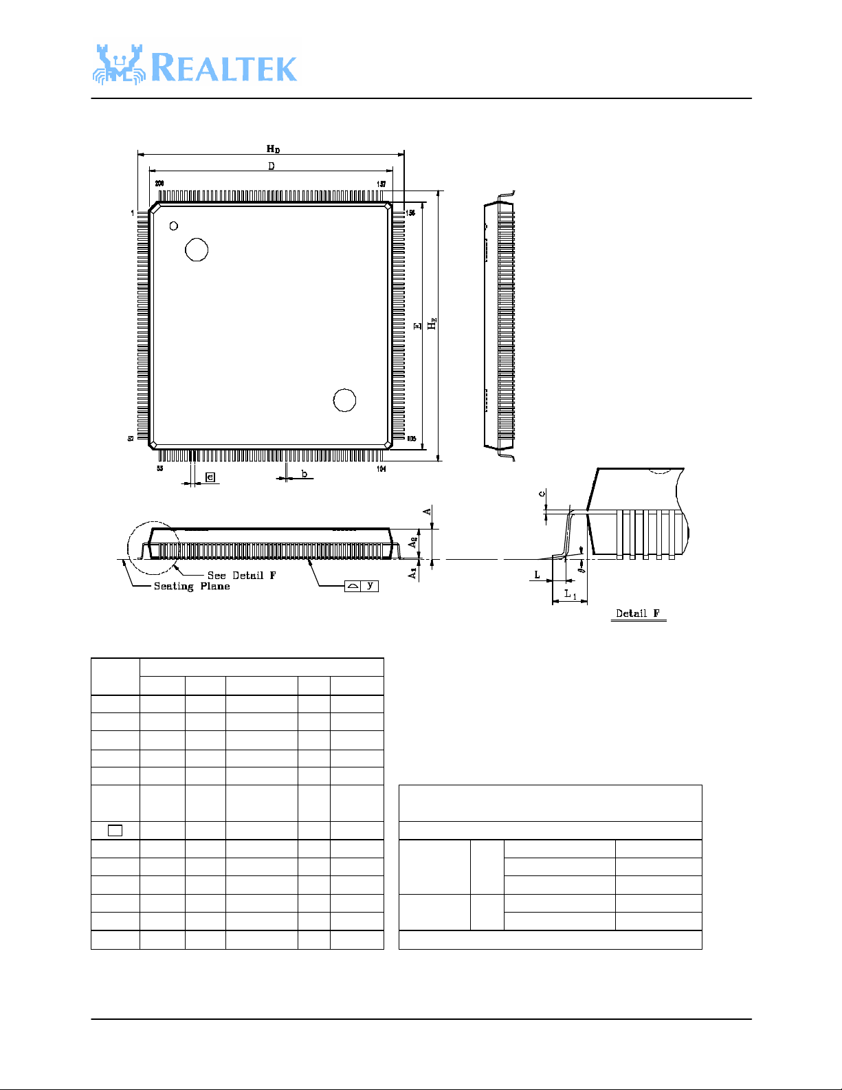
RTL8181
Package outline for 208 LQFP(28*28*1.4mm)
Note:
Symbol Dimension in inch Dimension in mm 1.Dimension D & E do not include interlead
Min Typ Max Min Typ Max flash.
A 0.136 0.144 0.152 3.45 3.65 3.85
A1 0.004 0.010 0.036 0.10 0.25 0.91 protrusion/intrusion.
A2 0.119 0.128 0.136 3.02 3.24 3.46
b 0.004 0.008 0.012 0.10 0.20 0.30
c 0.002 0.006 0.010 0.04 0.15 0.26
D 1.093 1.102 1.112 27.75 28.00 28.25
E 1.093 1.102 1.112 27.75 28.00 28.25
e
0.012 0.020 0.031 0.30 0.50 0.80
HD 1.169 1.205 1.240 29.70 30.60 31.50
HE 1.169 1.205 1.240 29.70 30.60 31.50
L 0.010 0.020 0.030 0.25 0.50 0.75
L1 0.041 0.051 0.061 1.05 1.30 1.55
y - - 0.004 - - 0.10 DATE APR. 11.1997
0° - 12° 0° - 12°
?
2.Dimension b does not include dambar
3.Controlling dimension: Millimeter
4.General appearance spec. should be based
on final visual inspection spec.
TITLE : 208L QFP ( 28x28 mm**2 ) FOOTPRINT 2.6mm
PACKAGE OUTLINE DRAWING
LEADFRAME MATERIAL:
APPROVE DOC. NO. 530-ASS-P004
VERSION 1
PAGE 22 OF 22
CHECK DWG NO. Q208 - 1
REALTEK SEMI-CONDUCTOR CO., LTD
CONFIDENTIAL v1.0
49
Page 50
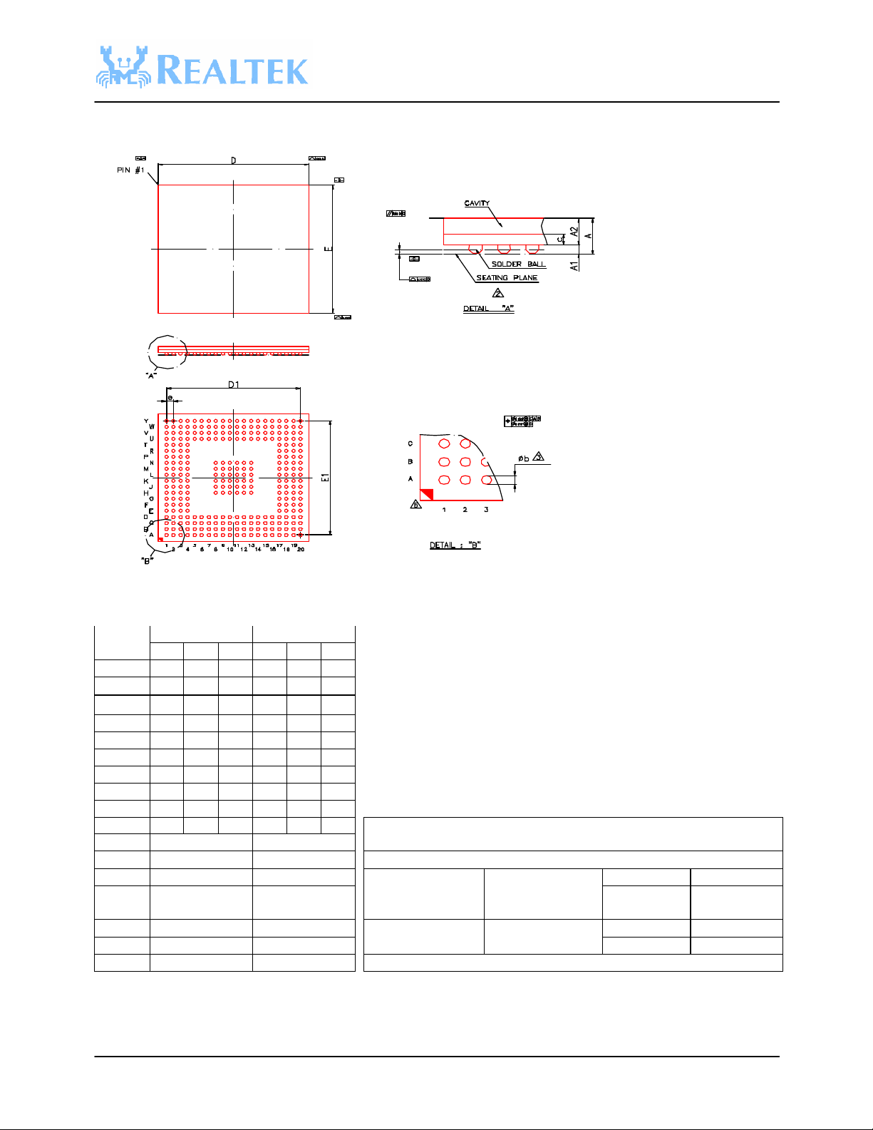
RTL8181
Package outline for TFBGA 292 BALL(17*17 mm)
Symbol Dimension in mm Dimension in inch
Min Nom Max Min Nom Max 3. DIMENSION b IS MEASURED AT THE MAXIMUM SOLDER BALL
A
A1 0.25 0.30 0.35 0.010 0.012 0.014 4. THERE SHALL BE A MINIMUM CLEARANCE OF 0.25mm BETWEEN THE
A2 0.84 0.89 0.94 0.033 0.035 0.037 EDGE OF THE SOLDER BALL AND THE BODY EDGE.
D 16.90 17.00 17.10 0.665 0.669 0.673 6. THE PATTERN OF PIN 1 FIDUCIAL IS FOR REFERENCE ONLY.
E 16.90 17.00 17.10 0.665 0.669 0.673
D1 --- 15.20 --- --- 0.598 ---
E1 --- 15.20 --- --- 0.598 ---
aaa 0.10 0.004
bbb 0.10 0.004 SUBSTRATE MATERIAL: BT RESIN
ccc 0.12 0.005 APPR. DWG NO..
ddd 0.15 0.006 ENG. Rev NO
eee 0.08 0.003 QM. PRODUCT CODE
MD/ME 20/20 20/20 CHK. DATE.
--- --- 1.30 --- --- 0.051 DIAMETER, PARALLEL TO PRIMARY DATUM C.
c 0.32 0.36 0.40 0.
e --- 0.80 --- --- 0.031 ---
b 0.35 0.40 0.45 0.014 0.016 0.018 TITLE : 292LD TFBGA ( 17x17mm) PACKAGE OUTLINE
DWG. SHT No.
REALTEK SEMI-CONDUCTOR CO., LTD
0.014 0.016 5. REFERENCE DOCUMENT : JEDEC MO-205.
013
1. CONTROLLING DIMENSION : MILLIMETER
2. PRIMARY DATUM C AND SEATING PLANE ARE DEFINED BY THE
SPHERICAL CROWNS OF THE SOLDER BALLS.
CONFIDENTIAL v1.0
50
 Loading...