

Page 1
查询RT9818A-49GU3供应商
Micro-Power Voltage Detectors
RT9818
General Description
The RT9818 is a micro-power voltage detector
supervising the power supply voltage level for
microprocessors (μP) or digital systems. It provides
internally fixed threshold levels with 0.1V per step ra nging
from 1.2V to 5V , which covers most digital applications. It
features low supply current of 3μA. The RT9818 performs
supervisory function by sending out a reset signal
whenever the V
level. This reset signal will last the whole period before
VDD recovering. Once VDD recovered upcrossing the
threshold level, the reset signal will be released after a
certain delay time. RT9818 is provided in SC-82, SC-70-3,
voltage falls below a preset threshold
DD
Features
zz
z Internally Fixed Threshold 1.2V to 5V in 0.1V Step
zz
zz
z High Accuracy
zz
zz
z Low Supply Current 3
zz
zz
z No External Components Required
zz
zz
z Quick Reset within 20
zz
zz
z Built-in Recovery Delay Include 0ms, 55ms, 220ms,
zz
450ms Options
zz
z Low Functional Supply Voltage 0.9V
zz
zz
z N-Channel Open-Drain Output
zz
zz
z Small SC-82, SC-70-3, SOT-23-3, SOT-23-5, SOT-89
zz
Packages
zz
z RoHS Compliant and 100% Lead (Pb)-Free
zz
±±
±1.5%
±±
μμ
μA
μμ
μμ
μs
μμ
SOT-23-3, SOT -23-5 and SOT -89 packages.
Applications
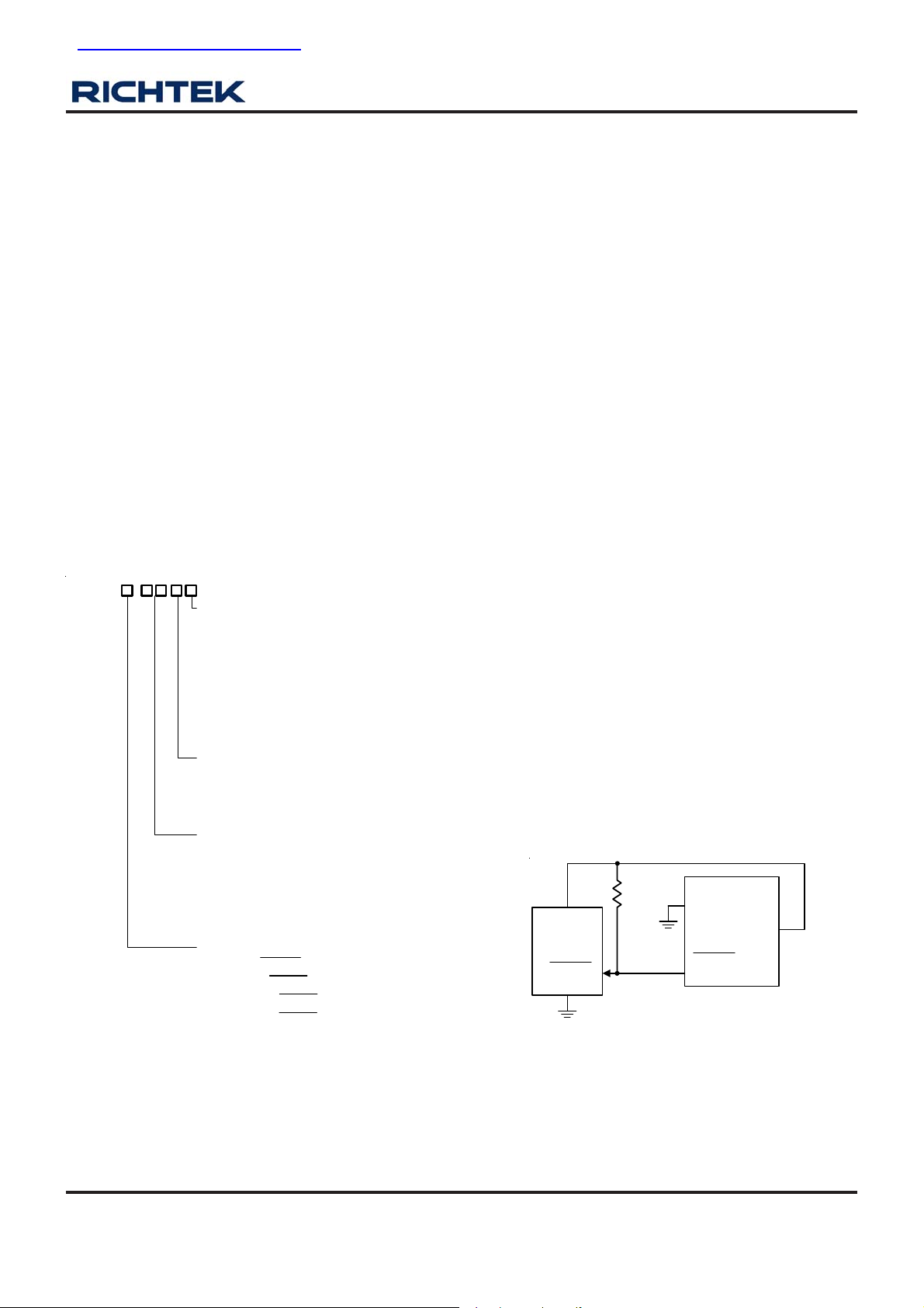
Ordering Information
RT9818
DS9818-05 March 2007 www.richtek.com
Package Type
U3 : SC-70-3
V : SOT-23-3
VL : SOT-23-3 (L-Type)
B : SOT-23-5
X : SOT-89
Y : SC-82
YR : SC-82 (R-Type)
Operating Temperature Range
P : Pb Free with Commercial Standard
G : Green (Halogen Free with Commer cial Standard)
Threshold Voltage
12 : 1.2V
13 : 1.3V
:
49 : 4.9V
50 : 5.0V
Reset Active Timeout Period
A = 0ms
(RESET)
B = 55ms (RESET)
C = 220ms (RESET)
D = 450ms (RESET)
E = 0ms (RESET)
F = 55ms (RESET)
G = 220ms (RESET)
H = 450ms (RESET)
z Computers
z Controllers
z Intelligent Instruments
z Critical μP and μC Power Monitoring
z Portable/Battery-Powered Equipment
Marking Information
For marking information, contact our sales representative
directly or through a RichTek distributor located in your
area, otherwise visit our website for detail.
Typical Application Circuit
100k
Pull Up
VDD
μP
RESET/
RESET
Note :
RichTek Pb-free and Green products are :
`RoHS compliant and compatible with the current require ments of IPC/JEDEC J-STD-020.
`Suitable for use in SnPb or Pb-free soldering processes.
`100%matte tin (Sn) plating.
RT9818
GND
VDD
RESET/
RESET
1
Page 2
RT9818
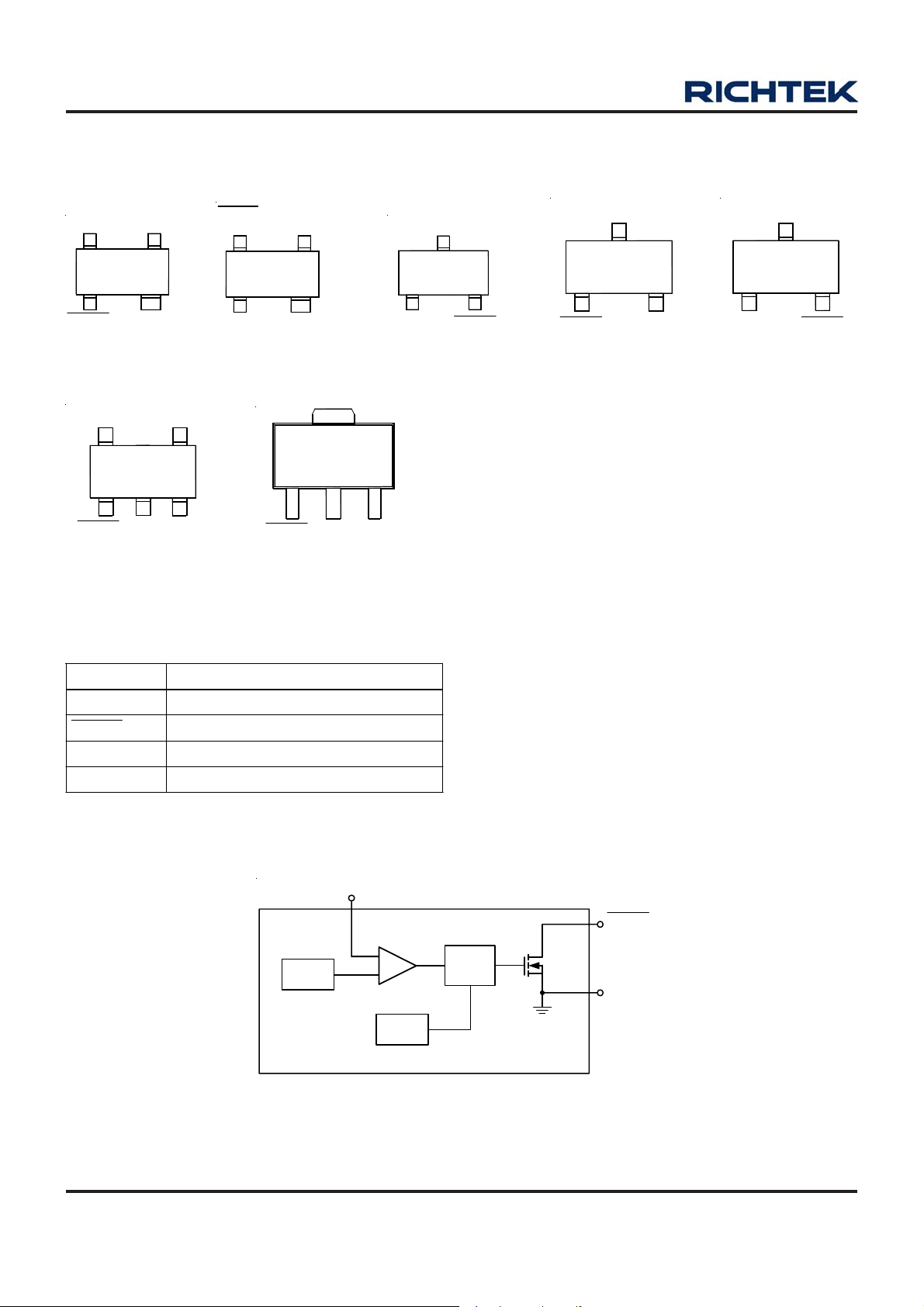
Pin Configurations
(TOP VIEW)
GND NC
4
1
RESET/
RESET
SC-82
5
RESET/
RESET
SOT-23-5
3
2
VDD
2
GNDVDD
RESET/
RESET
4
1
VDD
NC
3
2
GND
SC-82 (R-Type)
NCNC
4
31
RESET/
RESET
231
SOT-89
Functional Pin Description
VDD
3
1
GND
2
RESET/
RESET
SOT-23-3 (L-Type)
1
GND
VDD
3
RESET/
RESET
SC-70-3
VDD
3
2
1
RESET/
RESET
2
GND
SOT-23-3
Note : There is no pin1 indicator on top mark for SC-82 type,
and pin 1 will be lower left pin when reading top mark from
left to right. Pin2 of SC-82 is wider than other pins.
GNDVDD
Pin Name Pin Function
GND Ground
RESET Active Low Open-Drain Reset Output
RESET Active High Open-Drain Reset Output
VDD Power Pin
Function Block Diagram
VDD
VSET
Threshold
Voltage Setting
CMP
POR
Power On Reset
Timer
RESET/
RESET
N MOS
GND
DS9818-05 March 2007www.richtek.com
2
Page 3
RT9818
Absolute Maximum Ratings (Note 1)
z T erminal V oltage (with Respe ct to GND)
VDD------------------------------------------------------------------------------------------------------------------------ −0.3V to 6.0V
z All Other Inputs -------------------------------------------------------------------------------------------------------- −0.3V to V
z Input Current, I
z Power Dissipation, P
----------------------------------------------------------------------------------------------------- 20mA
VDD
@ TA = 25°C
D
SC-70 / SC-82---------------------------------------------------------------------------------------------------------- 0.25W
SOT-23-3 ---------------------------------------------------------------------------------------------------------------- 0.4W
SOT-23-5 ---------------------------------------------------------------------------------------------------------------- 0.4W
SOT-89------------------------------------------------------------------------------------------------------------------- 0.55W
z Package Thermal Resistance (Note 4)
SC-70 / SC-82, θJA---------------------------------------------------------------------------------------------------- 400°C/W
SOT-23-3, θJA----------------------------------------------------------------------------------------------------------- 250°C/W
SOT-23-5, θJA----------------------------------------------------------------------------------------------------------- 250°C/W
SOT-89, θJA------------------------------------------------------------------------------------------------------------- 180°C/W
z Lead Temperature (Soldering, 10sec.)---------------------------------------------------------------------------- 260°C
z Storage T emperature Range ---------------------------------------------------------------------------------------- −65°C to 125°C
z ESD Susceptibility (Note 2)
HBM (Human Body Mode) ------------------------------------------------------------------------------------------ 2kV
MM (Ma chine Mode)-------------------------------------------------------------------------------------------------- 200V
DD
+0.3V
Recommended Operating Conditions (Note 3)
z Junction T emperature Range---------------------------------------------------------------------------------------- −40°C to 125°C
z Ambient T emperature Range---------------------------------------------------------------------------------------- −40°C to 85°C
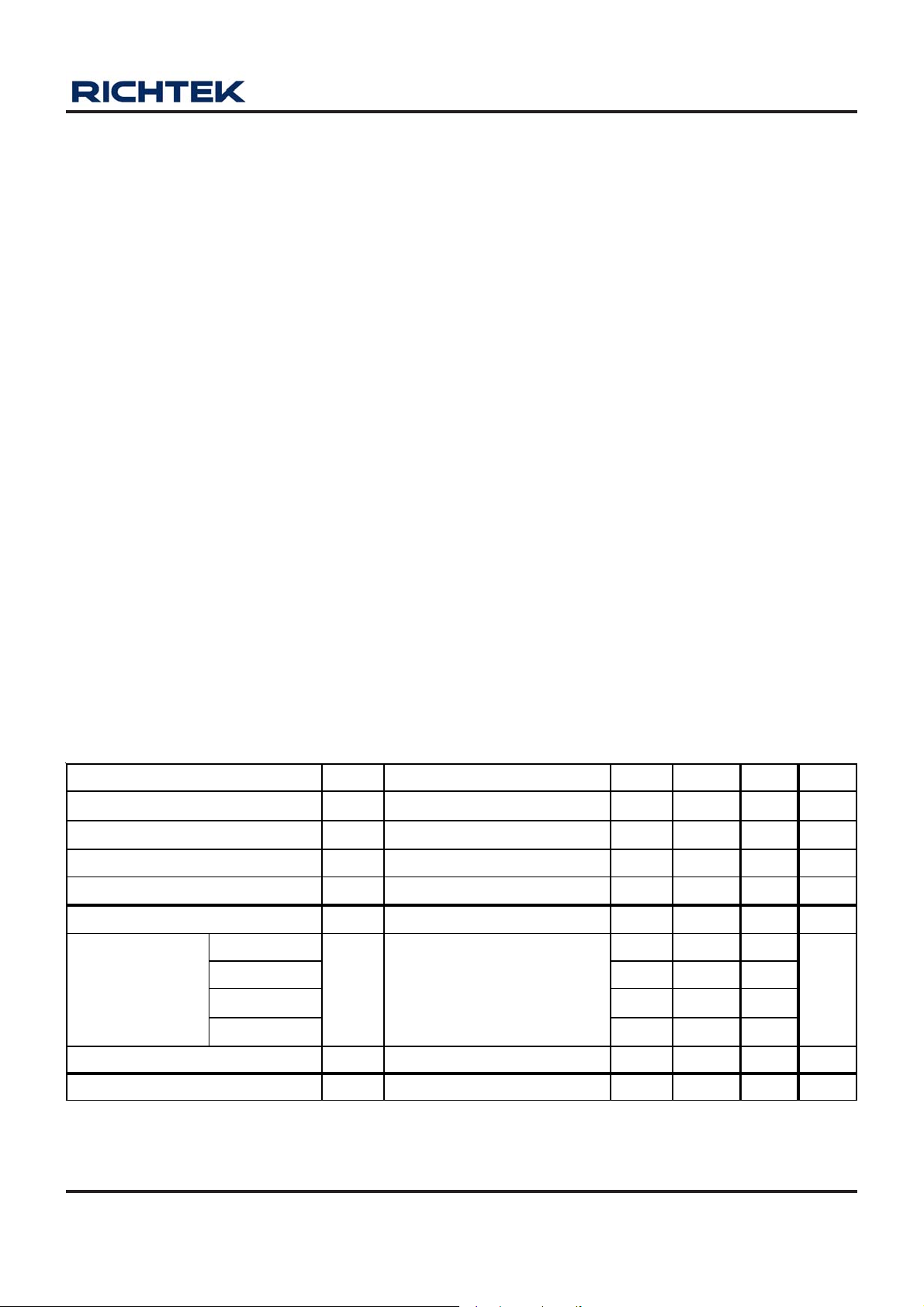
Electrical Characteristics
(VDD = 3V, unless otherwise specified)
Parameter Symbol Test Conditions Min Typ Max Units
Operating VDD (V
) Range VDD 0.9 -- 6
OUT
Supply Current IDD VTH = 3V , VDD = 4.5V TA = 27°C -- 3 8
Reset Threshold VTH TA = 27°C -- 1.2 to 5.0 --
Th reshold Voltage Accuracy ΔVTH T
= 27°C −1.5 -- +1.5 %
A
VDD Drop to Reset Delay tRD Drop = VTH -125mV -- 20 -- μs
-- 0 --
Reset Active Time
Out Period
RT9818A/E
RT9818B/F 35 55 75
VDD ≥ 1.02×VTH
t
RT9818C/G 143 220 297
RP
RT9818D/H 292 450 608
RESET Output Voltage Low (Note 5) VOL 3 = VDD < VTH I
Hysteresis Width V
0.01VTH V
HYS
>3.5 mA -- -- 0.4 V
SINK
V
μA
V
ms
DS9818-05 March 2007 www.richtek.com
3
Page 4

RT9818
Note 1. Stresses listed as the above “Absolute Maximum Ratings” may cause permanent damage to the device. These are
for stress ratings. Functional operation of the device at these or any other conditions beyond those indicated in the
operational sections of the specifications is not implied. Exposure to absolute maximum rating conditions for extended
periods may remain possibility to affect device reliability.
Note 2. Devices are ESD sensitive. Handling precaution recommended.
Note 3. The device is not guaranteed to function outside its operating conditions.
Note 4. θJA is measured in the natural convection at TA = 25°C on a low effective thermal conductivity test board of
JEDEC 51-3 thermal measurement standard.
Note 5. The voltage VOL can be calculated by VOL = VDD − Ir * R. Where R is the pull-up resistor and Ir is the current flowing
through the pull-up resistor. For typical application (R=100kΩ), V
is less than 0.2V.
OL
DS9818-05 March 2007www.richtek.com
4
Page 5
Typical Operating Characteristics
)
)
)
)
)
RT9818
Nch Driver Output Current vs. V
2.4
RT9818A-12
2
1.6
1.2
V
0.8
Output Current (mA
0.4
0
0 0.3 0.6 0.9 1.2 1.5
DD
V
DD
= 1.0V
DS
= 1.1V
VDS (V)
Nch Driver Output Current vs. V
120
RT9818A-45
100
80
60
40
Output Current (mA
20
0
012345
VDD = 4.4V
= 4.0V
= 3.5V
= 3.0V
= 2.5V
= 2.0V
= 1.5V
DS
VDS (V)
Nch Driver Output Current vs. V
60
RT9818C-30
50
V
V
DD
DD
= 2.0V
40
30
20
Output Current (mA
10
0
0 0.5 1 1.5 2 2.5 3 3.5
V
DD
= 1.5V
V
DD
= 2.5V
DS
= 2.8V
VDS (V)
Output Voltage vs. Input Voltage
7
RT9818
6
5
4
3
2
Output Volgate ( V)
1
0
0123456
1.2V
Inpu t Volgate ( V )
4.5V
Supply Current v s . Input Voltage
6
RT9818A-12
5
4
3
2
Supply Cur rent ( uA
1
0
0123456
80°C
25°C
-30°C
Inp ut Voltage (V)
4
3.5
3
2.5
2
1.5
1
Supply Cur rent (uA
0.5
0
Supply Current v s . Input Voltage
RT9818C-30
80°C
25°C
-30°C
0123456
Inp ut Voltage (V)
DS9818-05 March 2007 www.richtek.com
5
Page 6

RT9818
)
Supply Current v s . Input Voltage
4
RT9818A-45
3.5
3
2.5
2
1.5
1
Supply Cur rent (uA
0.5
0
0123456
80°C
25°C
-30°C
Inp ut Voltage (V)
Power-Down Reset Delay vs. Temperature
45
RT9818C-30
40
35
30
25
20
15
10
5
Power-Down Reset Delay (us)
0
-50 -25 0 25 50 7 5 100 125
V
= 200mV
DROP
Temperature
V
V
DROP
DROP
(°C)
= 150mV
= 250mV
Power-Down Reset Dela y vs. Temperature
14
RT9818A-12
12
10
V
8
6
4
2
DROP
= 200mV
V
V
DROP
DROP
= 150mV
= 250mV
Power-Down Reset Delay (us)
0
-50 -25 0 25 50 75 100 125
Temperature
(°C)
Power-Down Reset Delay vs. Temperatu re
45
RT9818A-45
40
35
30
25
20
15
10
5
Power-Down Reset Delay (us)
0
-50 -25 0 25 50 75 100 125
V
= 200mV
DROP
Temperature
V
V
(°C)
DROP
DROP
= 150mV
= 250mV
Reset Threshold Deviation vs. Temperature
6
RT9818
5.0V
5
4
3
Reset Threshold (V )
2
1
-50 -25 0 25 50 75 100 125
Temperature
4.5V
4.2V
2.2V
1.2V
(°C)
Nch Driver Sink Current vs. Input Voltage
40
RT9818C-30, V
35
30
(mA)
25
SINK
20
15
10
Sink Current I
5
0
00.511.522.533.5
= 0.5V
DS
25°C
Inpu t Volt age(V)
-30°C
80°C
DS9818-05 March 2007www.richtek.com
6
Page 7

RT9818
)
Nch Driver Sink Current vs. Input Voltage
50
RT9818A-45, V
40
DS
= 0.5V
-30°C
25°C
(mA)
30
SINK
80°C
20
Sink Current I
10
0
012345
Inpu t Voltage(V)
Power-Up Reset Time-Out vs. Temperature
100
RT9818A
80
Power-Up Reset Time-Out v s. Tem pe rature
500
RT9818C
400
V
= 2.9V
TH
300
V
200
100
TH
= 3.0V
Power-Up Reset Time-Out (ms)
0
-50 -25 0 25 50 75 100 125
Temperature
(°C)
Output Dela y Time vs. Load Capacitance
1000
RT9818
100
60
V
= 5.0V
TH
40
20
V
TH
= 4.5V
Power-Up Reset Time-Out (us)
0
-50 -25 0 25 50 75 100 125
160
140
120
100
80
60
40
20
Temperature
Nch Driver Output Current vs. V
RT9818G-31
(°C)
DS
VDD = 6.0V
= 5.5V
= 5.0V
= 4.5V
= 4.0V
= 3.5V
Nch Driver Output Current (mA) 1
0
0123456
VDS (V)
10
V
= 1.2V
TH
1
0.1
Output Delay Time (ms
V
= 4.5V
TH
0.01
0.0001 0.0010 0.0100 0.1000 1.0000
Load Capacitance (uF)
Nch Driver Output Current vs. Input Voltage
60
RT9818G-31
VDS = 0.5V
50
40
30
20
10
Nch Driver Output Current (mA) 1
0
0123456
Inp ut Voltage (V)
-30°C
25°C
80°C
DS9818-05 March 2007 www.richtek.com
7
Page 8

RT9818
)
)
Power Down Reset Time-Out vs. Temperature
500
RT9818G-31
400
300
200
100
Power Down Reset Time-Out (ms
0
-50 -25 0 25 50 75 100 125
Temperature
(°C)
Power-Down Reset Time-Out vs. Temperature
30
RT9818G-31
25
20
V
= 200mV
DROP
15
V
DROP
= 150mV
Output Voltage vs. Input Voltage
7
RT9818G-31
6
5
4
3
2
Output V oltage ( V )
1
0
0123456
Inpu t Volt age (V)
10
5
V
DROP
= 250mV
Power-Down Reset Time-Out (us
0
-50 -25 0 25 50 75 100 125
Temperature
(°C)
DS9818-05 March 2007www.richtek.com
8
Page 9

RT9818
Application Information
Multiple Supplies
Mainly , the pull-up connected to the R T9818 will connect to the supply voltage that is being monitored at the IC’s VDD
pin. However, some systems may use the open-drain output to level-shift from the monitored supply to reset circuitry
powered by some other supply .
Benefits of Highly Accurate Reset Threshold
Most μP supervisor ICs have reset threshold voltages between 1% and 1.5% below the value of nominal supply voltages.
This ensures a reset will not occur within 1% of the nominal supply, but will occur when the supply is 1.5% below
nominal.
DS9818-05 March 2007 www.richtek.com
9
Page 10

RT9818
Outline Dimension
D
C
e
A
b
Dimensions In M illimeters Dimensions In Inches
Symbol
Min Max Min Max
A 0.800 1.100 0.031 0.044
A1 0.000 0.100 0.000 0.004
B
A1
H
L
B 1.150 1.350 0.045 0.054
b 0.150 0.400 0.006 0.016
C 1.800 2.450 0.071 0.096
D 1.800 2.250 0.071 0.089
e 1.300 0.051
H 0.080 0.260 0.003 0.010
L 0.210 0.460 0.008 0.018
SC-70-3 Surface Mount Package
10
DS9818-05 March 2007www.richtek.com
Page 11

RT9818
D
e
C
b
A
e
Dimensions In Millimeters Dimensions In Inches
Symbol
Min Max Min Max
A 0.800 1.100 0.031 0.043
A1 0.000 0.100 0.000 0.004
B 1.150 1.350 0.045 0.053
B
b1
A1
H
L
b 0.150 0.400 0.006 0.016
b1 0.350 0.500 0.014 0.020
C 1.800 2.450 0.071 0.096
D 1.800 2.200 0.071 0.087
e 1.300 0.051
H 0.080 0.260 0.003 0.010
L 0.200 0.460 0.008 0.018
SC-82 Surface Mount Package
DS9818-05 March 2007 www.richtek.com
11
Page 12

RT9818
D
C
e
A
b
Dimensions In M illimeters Dimensions In Inches
Symbol
Min Max Min Max
A 0.889 1.295 0.035 0.051
A1 0.000 0.152 0.000 0.006
B 1.397 1.803 0.055 0.071
b 0.356 0.508 0.014 0.020
B
A1
H
L
C 2.591 2.997 0.102 0.118
D 2.692 3.099 0.106 0.122
e 1.803 2.007 0.071 0.079
H 0.080 0.254 0.003 0.010
L 0.300 0.610 0.012 0.024
SOT-23-3 Surface Mount Package
12
DS9818-05 March 2007www.richtek.com
Page 13

RT9818
H
D
L
C
b
A
e
Dimensions In Millimeters Dimensions In Inches
Symbol
Min Max Min Max
A 0.889 1.295 0.035 0.051
A1 0.000 0.152 0.000 0.006
B 1.397 1.803 0.055 0.071
b 0.356 0.559 0.014 0.022
C 2.591 2.997 0.102 0.118
D 2.692 3.099 0.106 0.122
B
A1
e 0.838 1.041 0.033 0.041
H 0.080 0.254 0.003 0.010
L 0.300 0.610 0.012 0.024
SOT-23-5 Surface Mount Package
DS9818-05 March 2007 www.richtek.com
13
Page 14

RT9818
D
D1
A
C
e
e
A
b
b1
b
B
C1
H
Dimensions In Millimeters Dimensions In Inches
Symbol
Min Max Min Max
A 1.397 1.600 0.055 0.063
b 0.356 0.483 0.014 0.019
B 2.388 2.591 0.094 0.102
b1 0.406 0.533 0.016 0.021
C 3.937 4.242 0.155 0.167
C1 0.787 1.194 0.031 0.047
D 4.394 4.597 0.173 0.181
D1 1.397 1.753 0.055 0.069
e 1.448 1.549 0.057 0.061
H 0.356 0.432 0.014 0.017
3-Lead SOT-89 Surface Mount Package
Richtek Technology Corporation
Headquarter
5F, No. 20, Taiyuen Street, Chupei City
Hsinchu, Taiwan, R.O.C.
Tel: (8863)5526789 Fax: (8863)5526611
14
Richtek Technology Corporation
Taipei Office (Marketing)
8F, No. 137, Lane 235, Paochiao Road, Hsintien City
Taipei County, Taiwan, R.O.C.
Tel: (8862)89191466 Fax: (8862)89191465
Email: marketing@richtek.com
DS9818-05 March 2007www.richtek.com
 Loading...