

Page 1
Synchronous-Rectified Buck MOSFET Drivers
RT9619/A
General Description
The RT9619/A is a high frequency, dual MOSFET driver
specifically designed to drive two power N-Channel
MOSFETs in a synchronous-rectified buck converter
topology. This driver combined with Richtek's series of
Multi-Phase Buck PWM controller f orm a complete corevoltage regulator solution for advanced micro-processors.
The RT9619/A drives both the lower/upper gate in a
synchronous-rectifier bridge with 12V. This drive-voltage
flexibility provides the advantage of opti mizing applications
involving trade-offs between switching losses and
conduction losses.
RT9619A has longer UGA TE/LGA TE deadti me which can
drive the MOSFET s with large gate RC value, avoiding the
shoot-through phenomenon. RT9619 is targeted to drive
low gate RC MOSFET s a nd performs better eff iciency .
The output drivers in the RT9619/A ca n eff iciently switch
power MOSFETs at frequency up to 500kHz. Switching
frequency above 500kHz has to take into account the
thermal dissipation of SOP-8 package. RT9619/A is
capable to drive a 3nF load with a 30ns rise time.
RT9619/A implements bootstrapping on the upper gate with
an external ca pacitor a nd an embedded diode. This
reduces
implementation complexity and allows the use of higher
performance, cost effective N-Channel MOSFETs. Adaptive
shoot-through protection is integrated to prevent both
MOSFET s from conducting si multa neously.
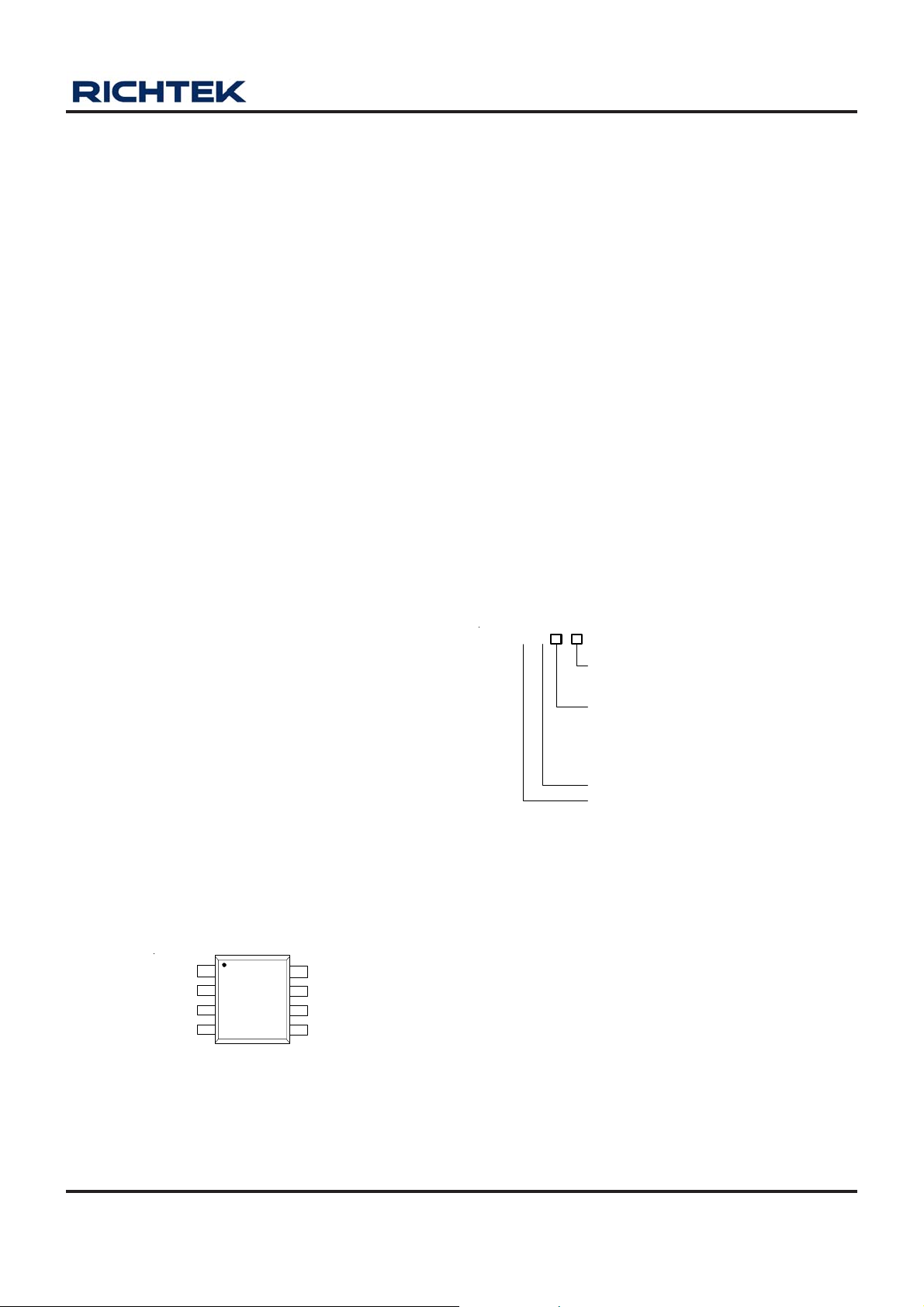
Pin Configurations
(TOP VIEW)
BOOT
PWM
NC
VCC
2
3
4
8
UGATE
7
PHASE
6
PGND
5
LGATE
Features
zz
Drives Two N-Channel MOSFET s
z
zz
zz
z Adaptive Shoot-Through Protection
zz
zz
z Embedded Boot Strapped Diode
zz
zz
z Supports High Switching Frequency
zz
zz
z Fast Output Rise T ime
zz
zz
z Small SOP-8 Package
zz
zz
z Tri-State Input for Bridge Shutdown
zz
zz
z Supply Under Voltage Protection
zz
zz
z Upper MOSFET Direct Shorted Protection
zz
zz
z RoHS Compliant and 100% Lead (Pb)-Free
zz
Applications
z Core V oltage Supplies for Desktop, Motherboard CPU
z High Frequency Low Profile DC-DC Converters
z High Current Low V oltage DC-DC Converters
Ordering Information
RT9619/A
Package Type
S : SOP-8
Operating Temperature Range
P : Pb Free with Commercial Standard
G : Green (Halogen Free with C om m er cial Standard)
Long Dead Time
Short Dead Time
Note :
RichTek Pb-free and Green products are :
`RoHS compliant and compatible with the current require ments of IPC/JEDEC J-STD-020.
`Suitable for use in SnPb or Pb-free soldering processes.
`100% matte tin (Sn) plating.
SOP-8
DS9619/A-04 March 2007 www.richtek.com
1
Page 2
RT9619/A
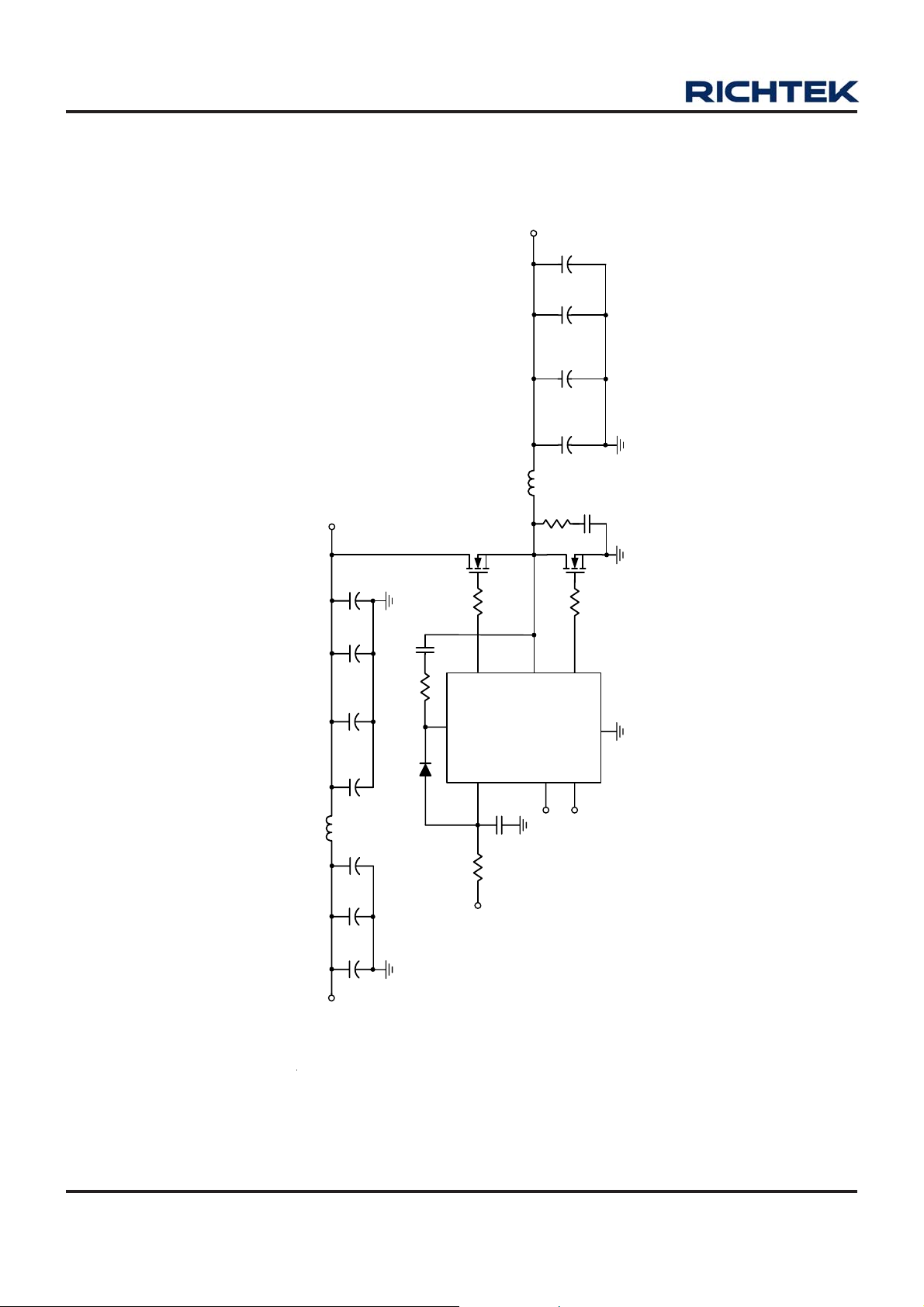
Typical Application Circuit
CORE
V
10uF
+
10uF
+
2200uF
+
C4 C5 C6 C7
2200uF
+
L2
IN
V
1uH
R5
C3
3.3nF
2.2
L1
2.2uH
C13 C14
10uF 10uF
C12
1000uF
1000uF
1000uF
10uF10uF
C8 C9 C10 C11
C2
R2
1uF
1
D1
Q1ATX_12V
R3
2.2
8
UGATE
1
BOOT
VCC
4
R1
10
C1
7
RT9619/A
1uF
PHASE
NC
3
R4
Q2
0
5
LGATE
6
PGND
PWM
2
PWM
ATX_12V
DS9619/A-04 March 2007www.richtek.com
2
Page 3
RT9619/A
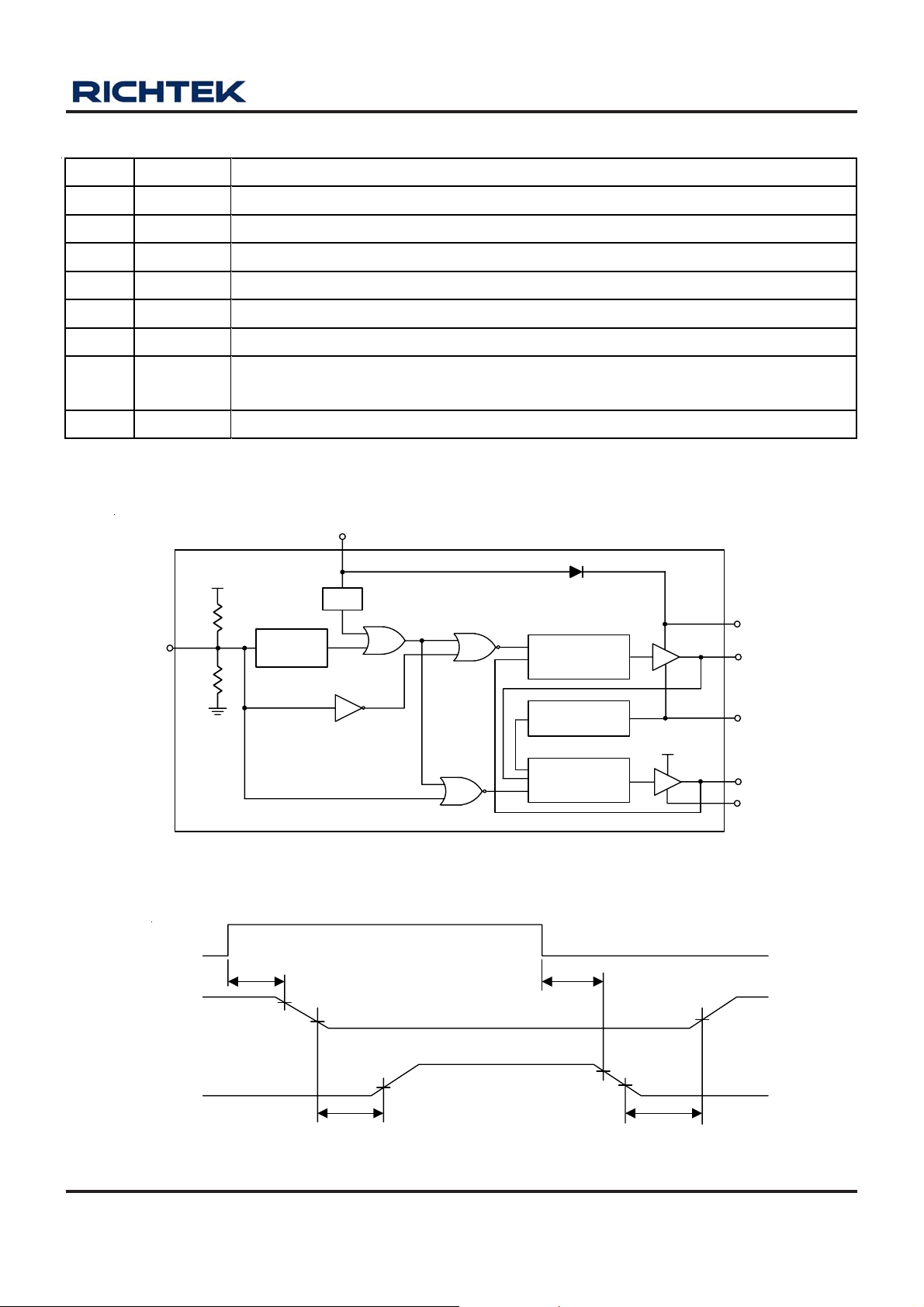
Functional Pin Description
Pin No. Pin Name Pin Function
1 BOOT Floating bootstrap su pply pin for upper gate drive.
2 PWM Input PWM signal for controlling the driver.
3 NC No Connection Pin.
4 VCC +12V Supply Voltag e .
5 LGATE Lower Gate Drive Output. Connected to gate of low-side power N-Channel MOSFET.
6 PGND Common Ground.
7 PHASE
Connected this pin to the source of the high-side MOSFET and the drain of the low-side
MOSFET.
8 UGATE Upper Gate Drive Output. Connected to gate of high-side power N-Channel MOSFET.
Function Block Diagram
VCC
Internal
5V
POR
PWM
R
Tri-State
Detect
R
Shoot-Through
Protection
Turn off Detect
VCC
Shoot-Through
Protection
BOOT
UGATE
PHASE
LGATE
PGND
Timing Diagram
PWM
LGATE
UGATE
DS9619/A-04 March 2007 www.richtek.com
t
pdlLGATE
90%
2V
2V
t
pdhUGATE
t
pdlUGATE
90%
2V
t
pdhLGATE
2V
3
Page 4
RT9619/A
Absolute Maximum Ratings (Note 1)
z Supply Voltage, V
z BOOT to PHASE ----------------------------------------------------------------------------------------- −0.3V to 15V
z BOOT to GND
DC------------------------------------------------------------------------------------------------------------ −0.3V to V
------------------------------------------------------------------------------------- −0.3V to 15V
CC
CC
+ 15V
< 200ns----------------------------------------------------------------------------------------------------- −0.3V to 42V
z PHASE to GND
DC------------------------------------------------------------------------------------------------------------ −5V to 15V
< 200ns----------------------------------------------------------------------------------------------------- −10V to 30V
z LGATE
DC------------------------------------------------------------------------------------------------------------ GND − 0.3V to VCC + 0.3V
< 200ns----------------------------------------------------------------------------------------------------- −2V to V
z UG ATE ------------------------------------------------------------------------------------------------------ V
< 200ns----------------------------------------------------------------------------------------------------- V
z PWM Input Voltage -------------------------------------------------------------------------------------- GND − 0.3V to 7V
z Power Dissipation, P
z SOP-8------------------------------------------------------------------------------------------------------- 0.625W
z Package Thermal Re sistance (Note 4)
@ T
D
= 25°C
A
PHASE
PHASE
+ 0.3V
CC
− 0.3V to V
− 2V to V
BOOT
BOOT
+ 0.3V
+ 0.3V
SOP-8, θJA------------------------------------------------------------------------------------------------- 160°C/W
z Lead T e mperature (Soldering, 10 sec.)-------------------------------------------------------------- 260°C
z Storage T emperature Range --------------------------------------------------------------------------- −40°C to 150°C
z ESD Susceptibility (Note 2)
HBM (Human Body Mode) ----------------------------------------------------------------------------- 2kV
MM (Ma chine Mode)------------------------------------------------------------------------------------- 200V
Recommended Operating Conditions
z Supply Voltage, V
z Junction T emperature Range--------------------------------------------------------------------------- 0°C to 125°C
z Ambient T emperature Range--------------------------------------------------------------------------- 0°C to 70°C
------------------------------------------------------------------------------------- 12V ±10%
CC
(Note 3)
Electrical Characteristics
(Recommended Operating Conditions, T
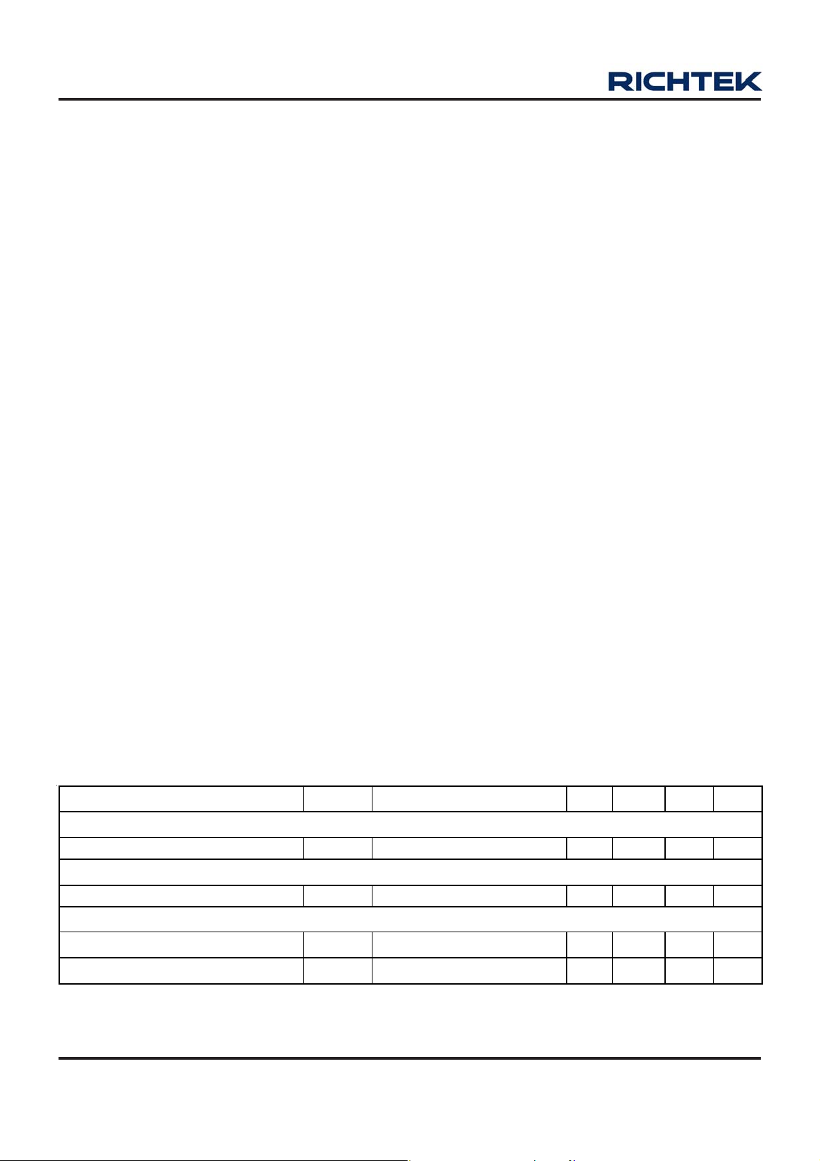
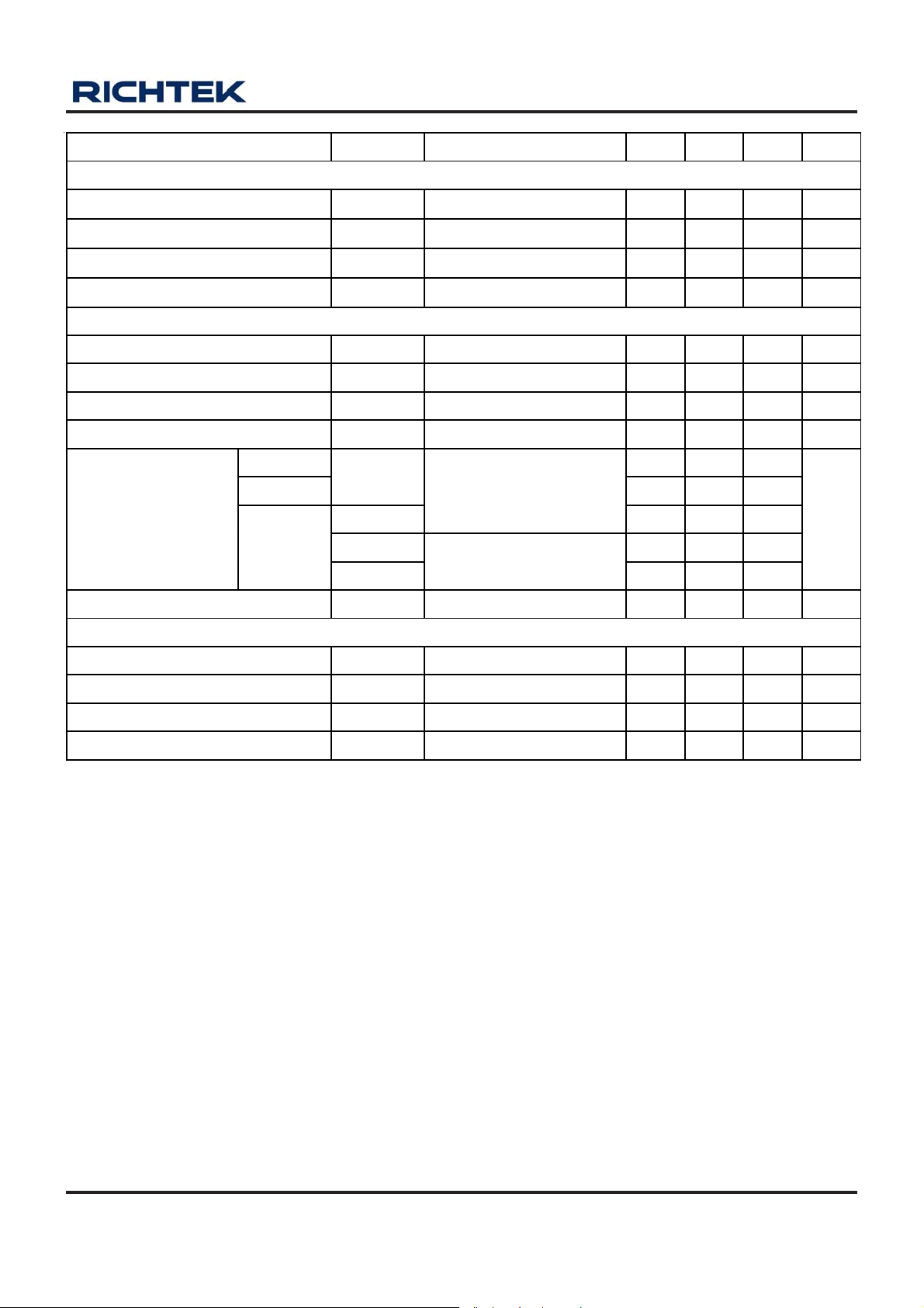
Parameter Symbol Test Conditions Min Typ Max Units
VCC Supply Voltage
Power Supply Voltage
VCC Supply Current
Power Supply Current
Power-On Reset
POR Threshold
Hysteresis
= 25°C unless otherwise specified)
A
V
CC
V
I
VCC
V
VCCrth
V
VCChys
7.3 -- 13.5 V
= 12V, PWM = 0V
BOOT
VCC Rising
-- 1 2.5 mA
5.5 6.4 7.3
-- 2.2 --
V
V
To be continued
DS9619/A-04 March 2007www.richtek.com
4
Page 5
PWM Input
RT9619/A
Parameter Symbol Test Conditions Min Typ Max Units
Maximum Input Current I
PWM Floating Voltage V
PWM Rising Threshold V
PWM Falling Threshold
V
PWM = 0V or 5V
PWM
VCC = 12V
PWMfl
PWMrth
PWMfth
-- 300 --
-- 2.4 --
3.2 3.6 3.9
1.1 1.3 1.5
μA
V
V
V
Timing
UGATE Rise Time t
UGATE Fall Time t
LGATE Rise Time t
LGATE Fall Time t
rUGATE
fUGATE
rLGATE
fLGATE
VCC = 12V, 3nF load -- 27 35 ns
VCC = 12V, 3nF load -- 32 45 ns
VCC = 12V, 3nF load -- 35 45 ns
VCC = 12V, 3nF load -- 27 38 ns
RT9619 -- 20 --
V
− V
BOOT
PHASE
See Timing Diagram
= 12V
-- 90 --
-- 15 --
ns
-- 20 -See Timing Diagram
-- 8 --
Propagation Delay
RT9619A
RT9619/A
t
pdhUGATE
t
pdlUGATE
t
pdhLGATE
t
pdlLGATE
Shutdown Window 1.5 -- 3.2 V
Output
UGATE Drive Source R
UGATE Drive Sink R
LGATE Drive Source R
LGATE Drive Sink R
Note 1. Stresses listed as the above “Absolute Maximum Ratings” may cause permanent damage to the device. These are for
stress ratings. Functional operation of the device at these or any other conditions beyond those indicated in the operational
sections of the specifications is not implied. Exposure to absolute maximum rating conditions for extended periods may
remain possibility to affect device reliability.
Note 2. Devices are ESD sensitive. Handling precaution recommended.
Note 3. The device is not guaranteed to function outside its operating conditions.
Note 4. θ
is measured in the natural convection at TA = 25°C on a low effective thermal conductivity test board of
JA
JEDEC 51-3 thermal measurement standard.
UGATEsr
UGATEsk
LGATEsr
LGATEsk
V
V
BOOT
BOOT
– V
– V
= 12V -- 1.9 3 Ω
PHASE
= 12V -- 1.4 3 Ω
PHASE
VCC = 12V -- 1.9 3 Ω
VCC = 12V -- 1.1 2.2 Ω
DS9619/A-04 March 2007 www.richtek.com
5
Page 6
RT9619/A
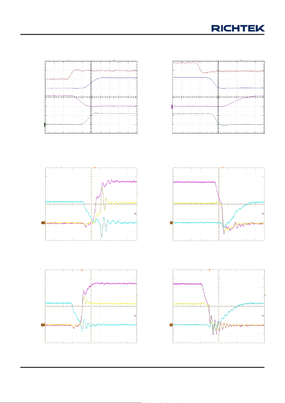
Typical Operating Characteristics
PWM
(5V/Div)
UGATE
(20V/Div)
LGATE
(10V/Div)
PHASE
(10V/Div)
PWM to Drive Waveform
No Load
Time (25ns/Div)
Dead Time
Full Load
UGATE
PWM
(5V/Div)
UGATE
(20V/Div)
LGATE
(10V/Div)
PHASE
(10V/Div)
PWM to Drive Waveform
No Load
Time (25ns/Div)
Dead Time
Full Load
UGATE
(5V/Div)
(5V/Div)
No Load
Time (20ns/Div)
Dead Time
PHASE
LGATE
UGATE
PHASE
LGATE
PHASE
(5V/Div)
LGATE
Time (20ns/Div)
Dead Time
No Load
UGATE
PHASE
(5V/Div)
LGATE
Time (20ns/Div)
6
Time (20ns/Div)
DS9619/A-04 March 2007www.richtek.com
Page 7
RT9619/A
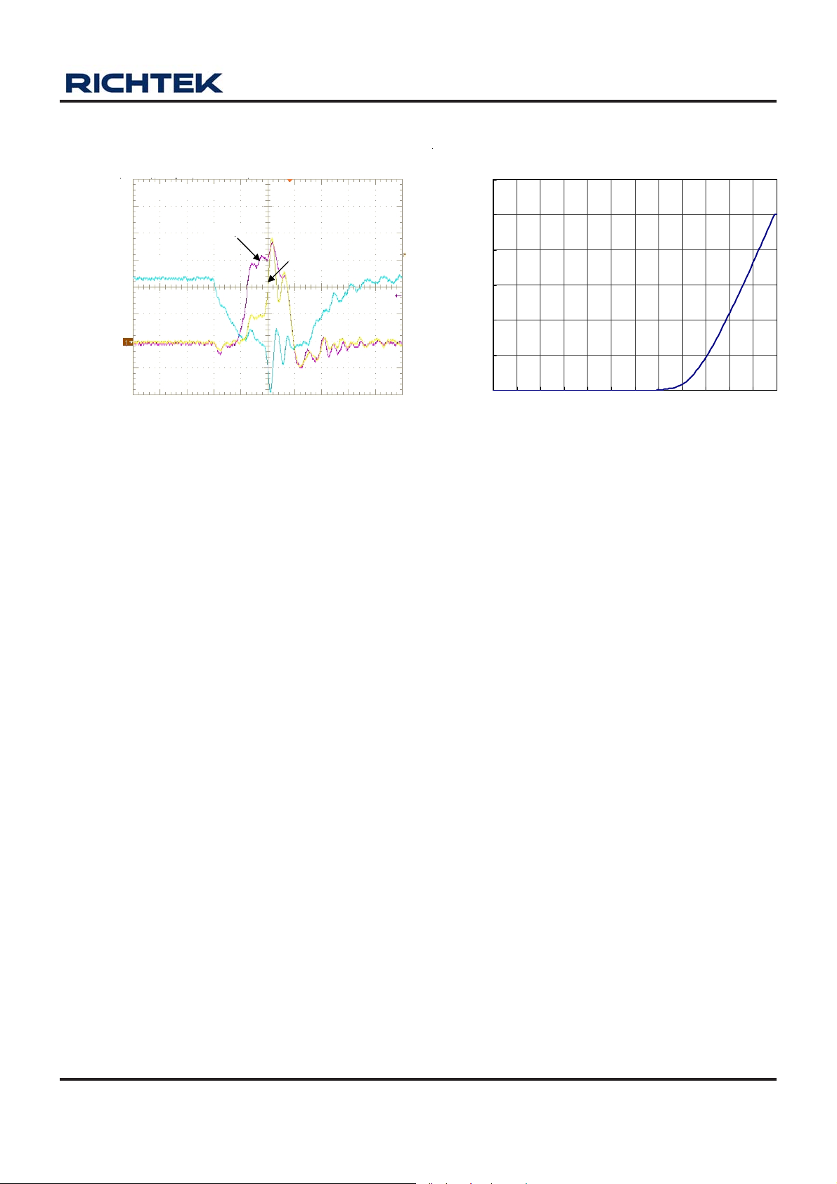
(5V/Div)
I
= 119A to 24A
OUT
LGATE
Short Pulse
UGATE
Time (20ns/Div)
PHASE
0.06
Internal Diode I-V Curve
0.05
0.04
0.03
Current (A)
0.02
0.01
0.00
0.0 0.1 0.2 0.3 0.4 0.5 0.6 0.7 0.8 0.9 1.0 1.1 1.2
Voltage (V)
DS9619/A-04 March 2007 www.richtek.com
7
Page 8
RT9619/A
Application Information
The RT9619/A is designed to drive both high side a nd low
side N-Channel MOSFET through externally input PWM
control signal. It has power-on protection function which
held UGATE and LGATE low before VCC up across the
rising threshold voltage. After the initi alization, the PWM
signal takes the control. The rising PWM signal first forces
the LGATE signal turn s low then UGATE sign al is allowed
to go high just after a non-overlapping ti me to avoid shootthrough current. The falling of PWM signal first forces
UGA TE to go low. When UGA TE a nd PHASE signal reach
a predetermined low level, LGA TE signal is allowed to turn
high.
The PWM signal is acted as "High" if above the rising
threshold and a cted as "Low" if below the falling threshold.
Any signal level enters and remains within the shutdown
window is considered a s "tri-state", the output drivers are
disabled and both MOSFET gates are pulled and held
low. If left the PWM signal floating, the pin will be kept
around 2.4V by the internal divider and provide the PWM
controller with a recognizable level.
Also to prevent the overlap of the gate drive s during LGATE
turn low and UGATE turn high, the non-overlap circuit
monitors the LGA TE voltage. When LGATE go below 1.2V,
UGA TE is allowed to go high.
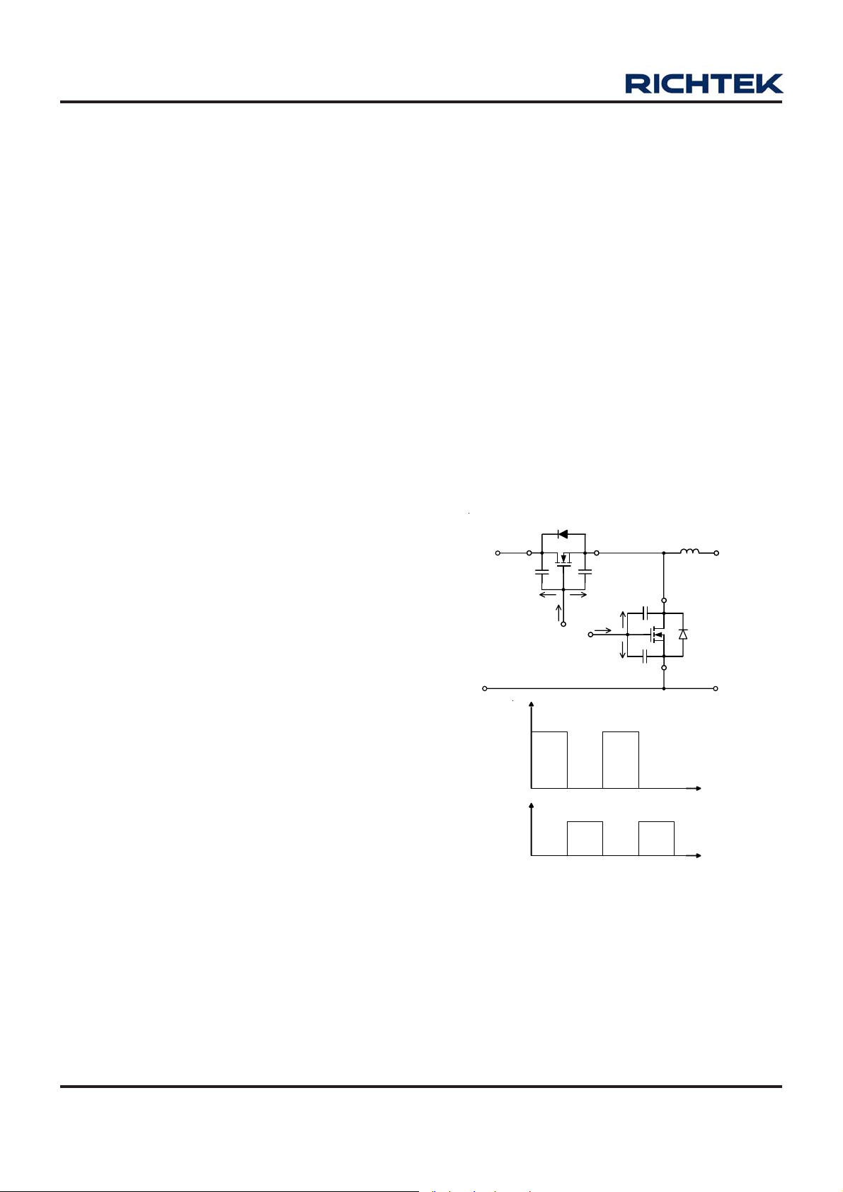
Driving Power MOSFET s
The DC input impedance of the power MOSFET is
extremely high. When Vgs at 12V (or 5V), the gate draws
the current only few nano-amperes. Thus once the gate
has been driven up to "ON " level, the current could be
negligible.
However, the capacitance at the gate to source terminal
should be considered. It requires relatively large currents
to drive the gate up and down 12V (or 5V) rapidly. It also
required to switch drain current on and off with the required
speed. The required gate drive currents are calculated a s
follows.
D1
V
d1
IN
Cgd1
s1
Cgs1
L
V
OUT
The RT9619/A typically operates at frequency of 200kHz
to 500kHz. It shall be noted that to place a 1N4148 or
schottky diode between the VCC and BOOT pin as shown
in the typical application circuit f or ligher efficiency.
Non-overlap Control
T o prevent the overla p of the gate drives during the UGA TE
turn low and the LGA TE turn high, the non-overla p circuit
monitors the voltages at the PHASE node and high side
gate drive (UGA TE-PHASE). When the PWM input signal
goes low, UGATE begins to turn low (after propagation
delay). Before LGATE can turn high, the non-overlap
protection circuit ensures that the monitored voltages have
gone below 1.2V . Once the monitored voltages fall below
1.2V , LGA TE begins to turn high. For short pulse condtion,
if the PHASE pin had not gone high after LGATE turns
low, the LGA TE ha s to wait f or 200ns before turn high. By
waiting for the voltages of the PHASE pin and high side
gate drive to fall below 1.2V, the non-overlap protection
circuit ensures that UGATE is low before LGATE turns
high.
Cgd2
Cgs2
d2
D2
s2
GND
t
t
Igs1
Igd1
Ig1
g
V
g1
V
PHASE
V
g2
1
+12V
g2
12V
Igd2
Ig2
Igs2
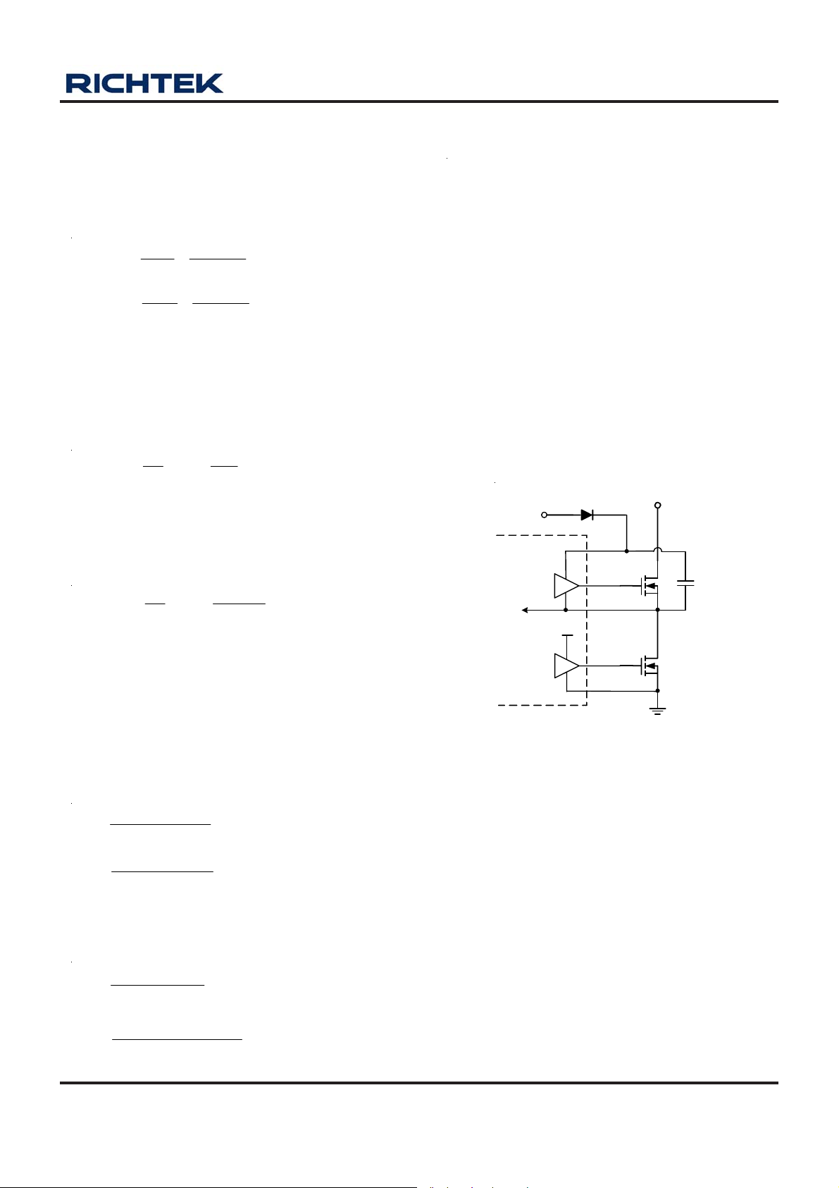
Figure 1. Equivalent Circuit and Associated W aveforms
In Figure 1, the current Ig1 and Ig2 are required to move the
gate up to 12V. The operation consists of charging C
and Cgs. C
gs1
and C
are the ca pacitances from gate to
gs2
source of the high side and the low side power MOSFET s,
respectively . In general data sheets, the Cgs is referred as
"C
" which is the input cap acitance. C
iss
gd1
and C
gd2
are the
capacitances from gate to drain of the high side and the
gd
DS9619/A-04 March 2007www.richtek.com
8
Page 9
RT9619/A
low side power MOSFET s, respectively and referred to the
data sheets as "C
exa mple, t
r1
and t
" the reverse trans fer capa citance. For
rss
are the rising time of the high side and
r2
the low side power MOSFETs respectively, the required
current I
gs1
CI
CI
and I
gs1gs1
gs1gs2
are showed below :
gs2
,
dVg1
dt
dVg2
dt
gs1
==
t
r1
gs1
==
t
×
12C
×
12C
r2
(1)
(2)
Before driving the gate of the high side MOSFET up to
12V (or 5V), the low side MOSFET ha s to be of f; a nd the
high side MOSFET is turned off before the low side is
turned on. From Figure 1, the body diode "D2" had been
turned on before high side MOSFET s turned on.
dV
CI ==
dt
Before the low side MOSFET is turned on, the C
been charged to VIN. Thus, as C
and g
is charged up to 12V, the required current is
2
dV
CI
dt
==
12V
C
gd1gd1gd1
t
r1
reverses its polarity
gd2
12VVi
C
+
gd2gd2gd2
t
r2
gd2
(3)
have
(4)
It is helpful to calculate these currents in a typical case.
Assume a synchronous rectified buck converter, input
voltage V
is PHB83N03LT whose C
t
= 14ns. The low side MOSFET is PHB95N03LT whose
r
C
iss
= 12V , Vg1 = Vg2 = 12V . The high side MOSFET
IN
= 2200pF , C
= 500pF and t
rss
= 1660pF, C
iss
= 30ns, from the equation
r
rss
= 380pF, and
(1) and (2) we ca n obtain
-12
12101660
I
I
gs1
gs2
××
=
1014
×
=
1030
×
=
9-
12-
12102200
××
=
9-
(A) 1.428
(A) 0.88
(5)
(6)
the total current required from the gate driving source is
gd1gs1g1
gd2gs2g2
=+=+=
=+=+=
(A) 1.7540.326)(1.428III
(A) 1.280.4)(0.88II I
(9)
(10)
By a similar calculation, we can also get the sink current
required from the turned off MOSFET .
Select the Bootstrap Capacitor
Figure 2 shows part of the bootstrap circuit of R T9619/A.
The V
(the voltage difference between BOOT a nd PHASE
CB
on RT9619/A) provides a voltage to the gate of the high
side power MOSFET. This supply needs to be ensured
that the MOSFET can be driven. For this, the ca pa citance
CB has to be selected properly . It is determined by f ollowing
constraints.
V
IN
C
+
B
V
CB
-
V
CC
1N4148
BOOT
UGATE
PHASE
LGATE
PGND
V
CC
Figure 2. Part of Bootstrap Circuit of RT9619/A
In practice, a low value capacitor CB will lead the overcharging that could damage the IC. Therefore to minimize
the risk of overcharging and reducing the ripple on VCB,
the bootstrap capacitor should not be smaller than 0.1μF,
and the larger the better . In general design, using 1μF can
provide better performance. At lea st one low-ESR capa citor
should be used to provide good local de-coupling. Here, to
adopt either a cera mic or tantalum capa citor is suitable.
from equation. (3) and (4)
-12
1210380
I
=
gd1
I
=
gd2
DS9619/A-04 March 2007 www.richtek.com
××
=
9-
1014
×
12-
1030
×
12)(1210500
+××
9-
(A) 0.326
=
(A) 0.4
(7)
(8)
Power Dissipation
For not exceeding the maximum allowable power
dissipation to drive the IC beyond the maximum
recommended operating junction temperature of 125°C, it
is necessary to calculate power dissipation a ppro-priately .
9
Page 10
RT9619/A
This dissipation is a function of switching frequency and
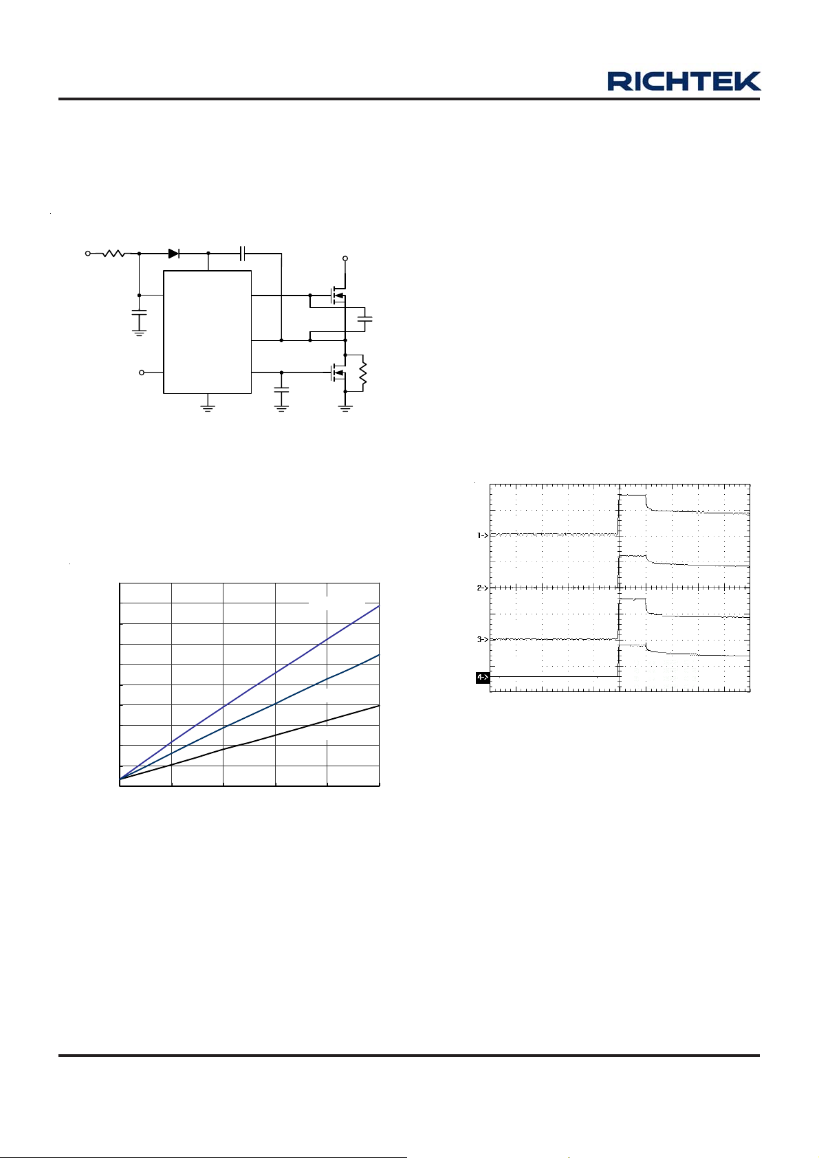
total gate charge of the selected MOSFET . Figure 3 shows
the power dissipation test circuit. C
and CU are the UGA TE
L
and LGATE load capacitors, respectively. The bootstrap
cap acitor value is 1μF.
C
BOOT
BOOT
UGATE
PHASE
LGATE
1uF
2N7002
C
L
3nF
+12V
2N7002
C
3nF
20
U
+12V
10
1uF
PWM
1N4148
VCC
RT9619/A
VIN
PGND
Figure 3. Test Circuit
Figure 4 shows the power dissipation of the RT9619/A a s
a function of frequency and load ca pa citance. The value of
the CU and CL are the same and the frequency is varied
from 100kHz to 1MHz.
T
= (160°C/W x 100mW) + 25°C = 41°C (11)
J
where the ambient temperature is 25°C.
The method to improve the thermal tran sfer is to increa se
the PCB copper area around the RT9619/A first. Then,
adding a ground pad under IC to transfer the heat to the
peripheral of the board.
Over-Voltage Protection Function at Power-On
An unique feature of the RT9619/A driver is the addition of
over-voltage protection in the event of upper MOSFET direct
shorted before power-on. The RT9619/Adetects the fault
condition during initial start-up, the internal power-on OVP
sense circuitry will ra pidly drive the output lower MOSFET
on before the multi-pha se PWM controller ta kes control.
Figure 5 shows the measured waveforms with the high
side MOSFET directly shorted to 12V.
(2V/Div)
VCC
Power Dissipation vs. Frequency
1000
900
800
700
600
500
400
300
200
Power Dissipation (mW)
100
0
0 200 400 600 800 1000
CU=CL=3nF
CU=CL=2nF
CU=CL=1nF
Frequency (kHz)
Figure 4. Power Dissipation vs. Frequency
The operating junction temperature can be calculated from
the power dissipation curves (Figure 4). Assume
VCC=12V, operating frequency is 200kHz and the
CU=CL=1nF which emulate the input cap acitances of the
high side and low side power MOSFETs. From Figure 4,
the power dissipation is 100mW. For RT9619/A, the
package thermal resista nce θ
is 160°C/W , the operating
JA
junction temperature is calculated as :
(2V/Div)
PHASE
(2V/Div)
LGATE
V
CORE
(2V/Div)
Time (50ms/Div)
Figure 5. Waveforms at High Side MOSFET Shorted
Plea se note that the VCC trigger point to RT9619/A is at
3V , a nd the cla mped level on PHASE pin is at about 2.4V .
Obviously since the PHASE pin voltage increa ses during
initial start-up, the V
increases correspondingly, but
CORE
it would quickly drop-off followed by LGATE and VCC
decrea sed.
Layout Consideration
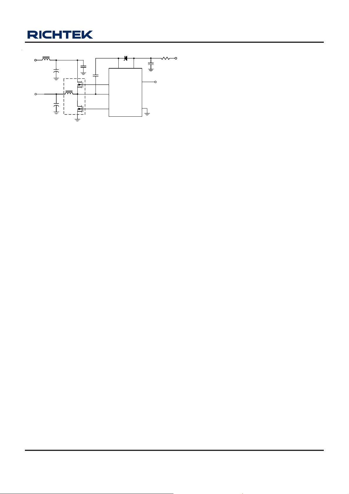
Figure 6 shows the schematic circuit of a two-phase
synchronous buck converter to implement the RT9619/A.
The converter operates from 5V to 12V of VIN.
10
DS9619/A-04 March 2007www.richtek.com
Page 11
RT9619/A
D1
14
VCC
BOOT
2
UGATE
PHASE
LGATE
VIN
RT9619/A
PGND
6
C4
1uF
PWM
V
V
12V
CORE
L1
IN
1.2uH
C1
1000uF
C3
1500uF
+
L2
+
2uH
Q1
Q2
C2
1uF
PHB83N03LT
PHB95N03LT
C
1uF
B
8
7
5
Figure 6. T wo-Phase Synchronous Buck Converter Circuit
When layout the PCB, it should be very careful. The powercircuit section is the most critical one. If not configured
properly , it will generate a large amount of EMI. The junction
of Q1, Q2, L2 should be very close.
Next, the trace from UGATE, and LGA TE should also be
short to decrease the noise of the driver output signals.
PHASE signals from the junction of the power MOSFET,
carrying the large gate drive current pulses, should be a s
heavy as the gate drive trace. The bypass capacitor C4
should be connected to PGND directly. Furthermore, the
bootstrap ca pa citors (CB) should always be placed a s close
to the pins of the IC a s possible.
R1
10
12V
DS9619/A-04 March 2007 www.richtek.com
11
Page 12
RT9619/A
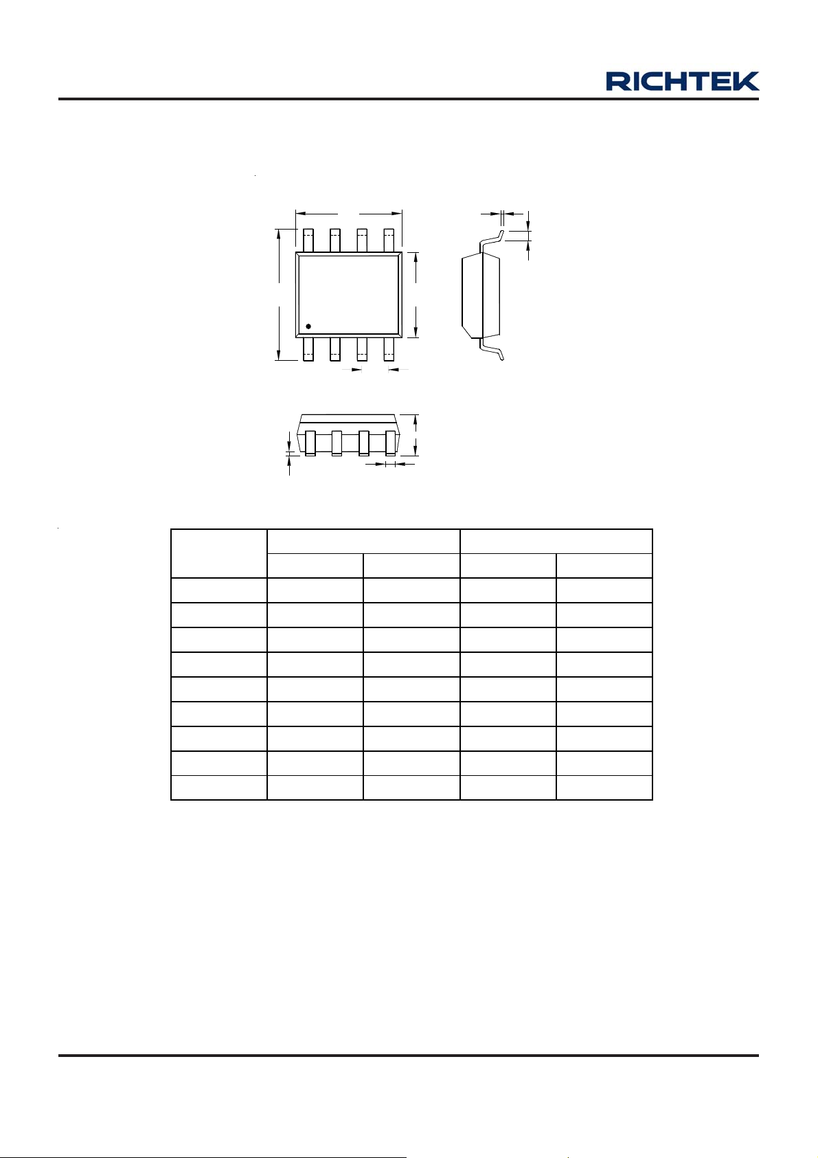
Outline Dimension
A
J
I
Dimensions In M illimeters Dimensions In Inches
Symbol
Min Max Min Max
A 4.801 5.004 0.189 0.197
B
F
C
D
H
M
B 3.810 3.988 0.150 0.157
C 1.346 1.753 0.053 0.069
D 0.330 0.508 0.013 0.020
F 1.194 1.346 0.047 0.053
H 0.170 0.254 0.007 0.010
I 0.050 0.254 0.002 0.010
J 5.791 6.200 0.228 0.244
M 0.400 1.270 0.016 0.050
Richtek Technology Corporation
Headquarter
5F, No. 20, Taiyuen Street, Chupei City
Hsinchu, Taiwan, R.O.C.
Tel: (8863)5526789 Fax: (8863)5526611
8-Lead SOP Plastic Package
Richtek Technology Corporation
Taipei Office (Marketing)
8F, No. 137, Lane 235, Paochiao Road, Hsintien City
Taipei County, Taiwan, R.O.C.
Tel: (8862)89191466 Fax: (8862)89191465
Email: [email protected]
12
DS9619/A-04 March 2007www.richtek.com
 Loading...