

Page 1
RT9602
Dual Channel Synchronous-Rectified Buck MOSFET Driver
General Description
The RT9602 is a dual power channel MOSFET driver
specifically designed to drive four power N-Channel
MOSFETs in a synchronous-rectified buck converter
topology. These drivers combined with RT9237/A and
RT9241A/B series of Multi-Phase Buck PWM
controllers provide a complete core voltage regulator
solution for advanced microprocessors.
The RT9602 can provide flexible gate driving for both
high side and low side drivers. This gives more
flexibility of MOSFET selection.
The output drivers in the RT9602 have the capability
to drive a 3000pF load with a 40nS propagation delay
and 80nS transition time. This device implements
bootstrapping on the upper gates with only a single
external capacitor required for each power channel.
This reduces implementation complexity and allows
the use of higher performance, cost effective, N-
Channel MOSFETs. Adaptive shoot-through protect-
ion is integrated to prevent both MOSFETs from
conducting simultaneously.
The RT9602 can detect high side MOSFET drain-to-
source electrical short at power on and pull the 12V
power by low side MOS and cause power supply to
go into over current shutdown to prevent damage of
CPU.
Features
Drives Four N-Channel MOSFETs
Adaptive Shoot-Through Protection
Internal Bootstrap Devices
Small 14-Lead SOIC Package
5V to 12V Gate-Drive Voltages for Optimal
Efficiency
Tri-State Input for Bridge Shutdown
Supply Under-Voltage Protection
Power ON Over-Voltage Protection
Applications
Core Voltage Supplies for Intel Pentium 4 and
AMD Athlon
High Frequency Low Profile DC-DC Converters
High Current Low Voltage DC-DC Converters
TM
Microprocessors
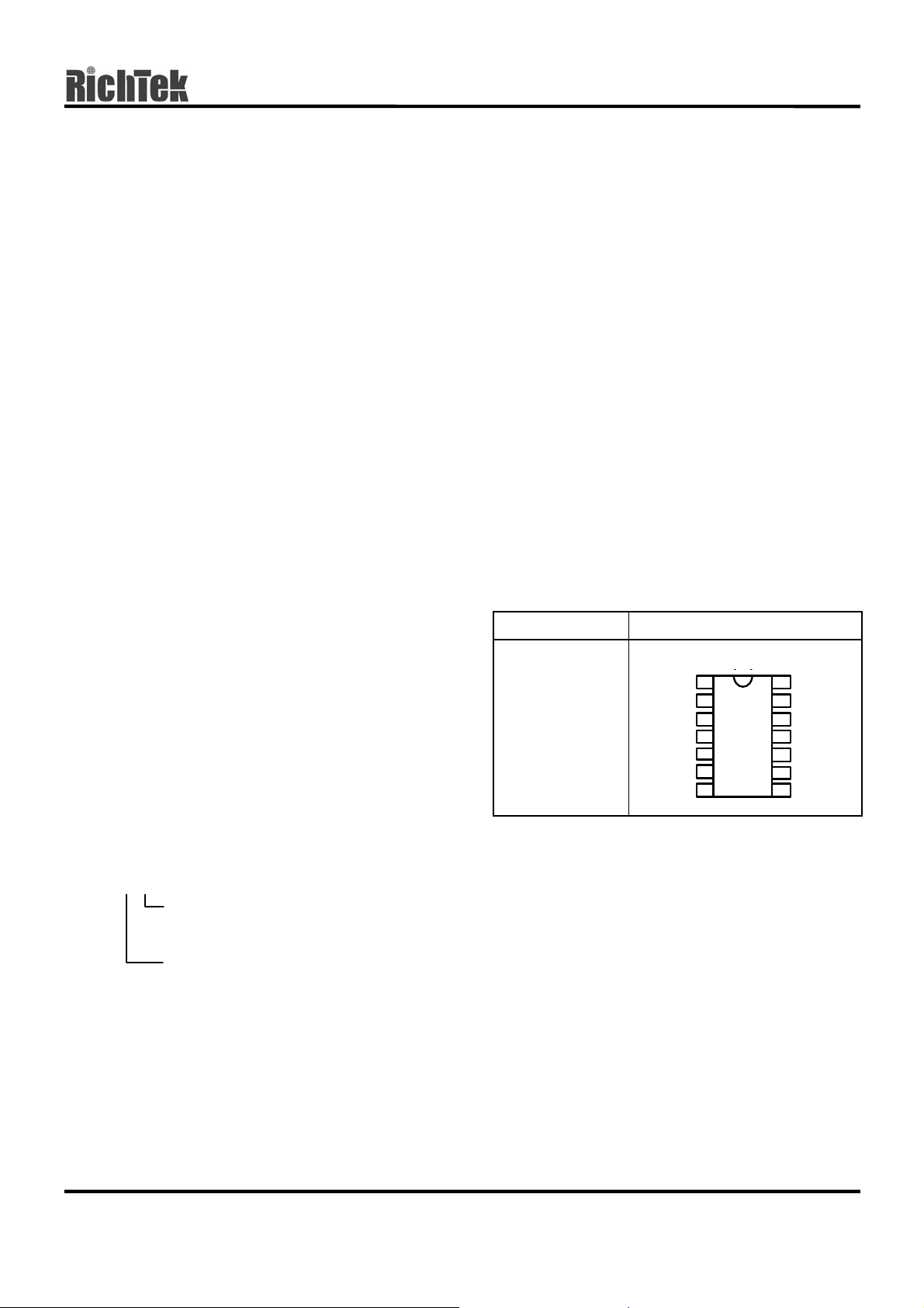
Pin Configurations
Part Number Pin Configurations
RT9602CS
(Plastic SOP-14)
PWM1
PWM2
LGATE1
PVCC
PGND
LGATE2
GND
TOP VIEW
1
2
3
4
5
6
7
14
13
12
11
10
9
8
VCC
PHASE1
UGATE1
BOOT 1
BOOT 2
UGATE2
PHASE2
Ordering Information
RT9602
DS9602-02 November 2002 www.richtek.com
1
Package Type
S : SOP-14
Operating Temperature Range
C: Commercial Standard
Page 2

RT9602
Pin Description
Pin No.
Pin Name Pin Function
1
PWM1 Channel 1 PWM Input
2
PWM2 Channel 2 PWM Input
3
GND Ground Pin
4
LGATE1 Lower Gate Drive of Channel 1
5
PVCC Upper and Lower Gate Driver Power Rail
6
PGND Lower Gate Driver Ground Pin
7
LGATE2 Lower Gate Drive of Channel 2
8 PHASE2
9
UGATE2 Upper Gate Drive of Channel 2
10
BOOT2 Floating Bootstrap Supply Pin of Channel 2
11
BOOT1 Floating Bootstrap Supply Pin of Channel 1
12
UGATE1 Upper Gate Drive of Channel 1
PHASE1
13
14
VCC Control Logic Power Supply
Connect this pin to phase point of channel 2.
Phase point is the connection point of high side MOSFET source and low side MOSFET drain
Connect this pin to phase point of channel 1.
Phase point is the connection point of high side MOSFET source and low side MOSFET drain
www.richtek.com DS9602-02 November 2002
2
Page 3
RT9602
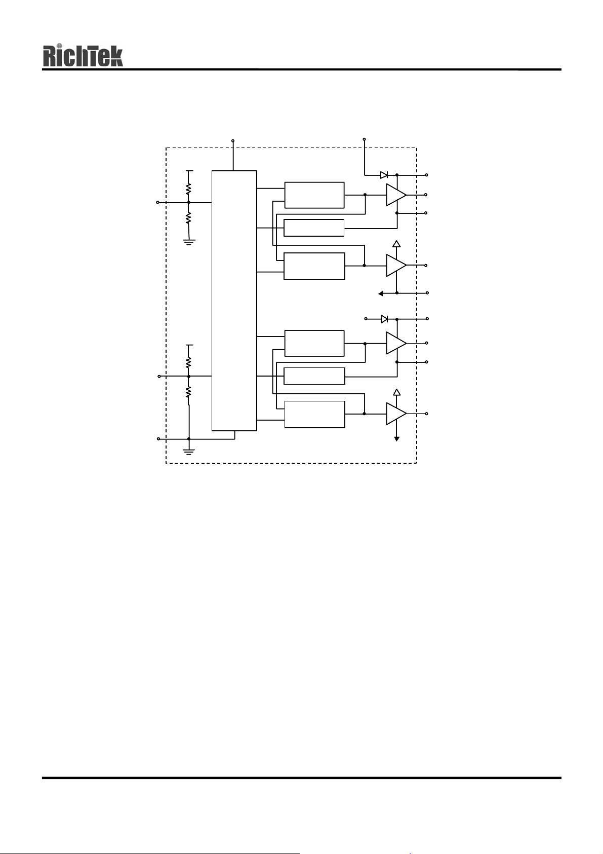
Function Block Diagram
Internal
Internal
5V
5V
40K
40K
PW M1
PW M1
40K
40K
Internal
Internal
5V
5V
40K
40K
PW M2
PW M2
40K
40K
VCC
VCC
Control
Control
Logic
Logic
Shoot-through
Shoot-through
Protection
Protection
Pow er-on OVP
Pow er-on OVP
Shoot-through
Shoot-through
Protection
Protection
Shoot-through
Shoot-through
Protection
Protection
Pow er-on OVP
Pow er-on OVP
Shoot-through
Shoot-through
Protection
Protection
PV C C
PV C C
PG N D
PG N D
PV C C
PV C C
PV C C
PV C C
PV C C
PV C C
BOOT1
BOOT1
UGA T E1
UGA T E1
PHASE1
PHASE1
LGATE1
LGATE1
PG N D
PG N D
BOOT2
BOOT2
UGA T E2
UGA T E2
PHASE2
PHASE2
LGATE2
LGATE2
GND
GND
PG N D
PG N D
DS9602-02 November 2002 www.richtek.com
3
Page 4
RT9602
Absolute Maximum Ratings
Supply Voltage (V
Supply Voltage (PV
BOOT Voltage (V
Input Voltage (V
UGATE V
LGATE GND − 0.3V to V
Package Thermal Resistance
SOP-14, θ
Ambient Temperature 0°C to 70°C
Junction Temperature 0°C to 125°C
Storage Temperature Range −40°C to 150°C
Lead Temperature (Soldering, 10 sec.) 260°C
ESD Level (Note)
127.67°C /W
JA
) 15V
CC
) VCC + 0.3V
CC
BOOT-VPHASE
) GND − 0.3V to 7V
PWM
) 15V
− 0.3V to V
PHASE
HBM 2KV
MM 200V
Electrical Characteristics
Parameter Symbol Test Conditions Min Typ Max Units
VCC Supply Current
BOOT
PVCC
+ 0.3V
+ 0.3V
Bias Supply Current
Power Supply Current
I
VCC
I
PVCC
= 250kHz, V
PWM
C
= 0.1µF, R
BOOT
f
= 250kHz, V
PWM
C
= 0.1µF, R
BOOT
PVCC
PHASE
PVCC
PHASE
= 12V,
= 20Ω
= 12V,
= 20Ω
-- 5.5 8 mA
-- 5.5 10 mA
f
Power-On Reset
VCC Rising Threshold
8.6 9.9 10.7 V
Hysteresis 0.6 1.35 -- V
PWM Input
Maximum Input Current
V
PWM
= 0 or 5V
80 127 150
µA
PWM Floating Voltage Vcc = 12V 1.1 2.1 3.7 V
PWM Rising Threshold 3.3 3.7 4.3 V
PWM Falling Threshold 1.0 1.26 1.5 V
UGATE Rise Time
LGATE Rise Time
UGATE Fall Time
LGATE Fall Time
UGATE Turn-Off Propagation Delay
LGATE Turn-Off Propagation Delay
V
PVCC
V
PVCC
V
PVCC
V
PVCC
V
VCC
V
VCC
= V
= V
= V
= V
= V
= V
= 12V, 3nF load
VCC
= 12V, 3nF load
VCC
= 12V, 3nF load
VCC
= 12V, 3nF load
VCC
= 12V, 3nF load
PVCC
= 12V, 3nF load
PVCC
-- 30 -- ns
-- 30 -- ns
-- 40 -- ns
-- 30 -- ns
-- 60 -- ns
-- 45 -- ns
Shutdown Window 1.26 -- 3.7 V
To be continued
www.richtek.com DS9602-02 November 2002
4
Page 5

Output
RT9602
Parameter Symbol Test Conditions Min Typ Max Units
Upper Drive Source
Upper Drive Sink
Lower Drive Source
Lower Drive Sink
R
UGATEVVCC
R
UGATEVVCC
R
LGATEVVCC
R
LGATEVVCC
= 12V, V
= 12V, V
= 12V, V
= V
PVCC
= 12V
PVCC
= 12V
PVCC
= 12V
PVCC
= 12V
-- 1.75 3.0
-- 2.8 5.0
-- 1.9 3.0
-- 1.6 3.0
Ω
Ω
Ω
Ω
Note: Devices are ESD sensitive, especially for PHASE and LGATE pins. Handling precaution recommended. The human
body model is a 100pF capacitor discharged through a 1.5KΩ resistor into each pin.
Operation Descriptions
The RT9602 has power on protection function which
held UGATE and LGATE low before VCC up cross
the rising threshold voltage. After the initialization, the
PWM signal takes the control. The rising PWM signal
first forces the LGATE signal turns low then UGATE
signal is allowed to go high just after a non-
overlapping time to avoid shoot-through current. The
falling of PWM signal first forces UGATE to go low.
When UGATE and PHASE signal reach a
predetermined low level, LGATE signal is allowed to
turn high. The non-overlapping function is also
presented between UGATE and LGATE signal
transient.
the PHASE low until the PHASE voltage goes below
1.5V. Such function can protect the CPU from
damage by some short condition happened before
power on, which is sometimes encountered in the
M/B manufacturing line.
The PWM signal is recognized as high if above rising
threshold and as low if below falling threshold. Any
signal level in this window is considered as tri-state,
which causes turn-off of both high side and low-side
MOSFET. When PWM input is floating (not
connected), internal divider will pull the PWM to 1.9V
to give the controller a recognizable level. The
maximum sink/source capability of internal PWM
reference is 60µA.
The PVCC pin provides flexibility of both high side
and low side MOSFET gate drive voltages. If 8V, for
example, is applied to PVCC, then high side
MOSFET gate drive is 8V to 1.5V (approximately,
internal diode plus series resistance voltage drop).
The low side gate drive voltage is exactly 8V.
The RT9602 implements a power on over-voltage
protection function. If the PHASE voltage exceeds
1.5V at power on, the LGATE would be turn on to pull
DS9602-02 November 2002 www.richtek.com
5
Page 6
RT9602
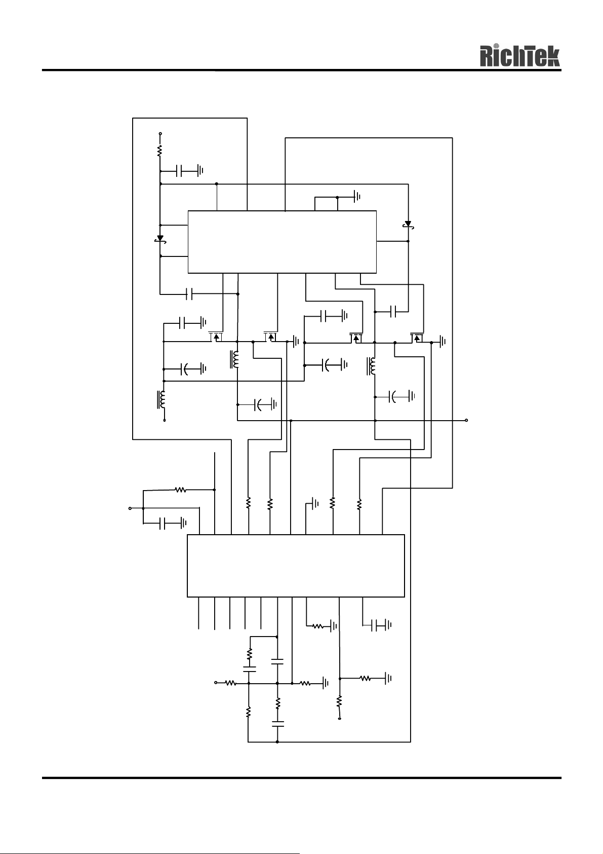
Typical Application Circuit
12V
12V
10Ω
10Ω
1µF
1µF
optional
optional
5
5
14
14
VCC
VCC
11
11
BOOT1
BOOT1
1µF
1µF
1µF
1µF
1
1
PWM1
PVCC
PWM1
PVCC
RT9602
RT9602
LGATE1
UGATE1
PHASE1
UGATE1
PHASE1
13
13
12
12
PHB83N 03LT
PHB83N 03LT
LGATE1
4
4
3
3
2
2
PWM2
PWM2
9
9
PHB95N 03LT
PHB95N 03LT
UGATE2
UGATE2
6
6
GND
GND
PGND
8
8
1µF
1µF
PGND
PHASE2
PHASE2
10
10
BOOT2
BOOT2
LGATE2
LGATE2
7
7
PHB83N 03LT
PHB83N 03LT
optional
optional
PHB95N03LT
PHB95N03LT
1000µF
1000µF
1.2µ H
1.2µ H
12V
12V
2µH
2µH
×1500µF
×1500µF
1000µF
1000µF
2µH
2µH
×1500µ F1µF
×1500µ F1µF
CORE
CORE
V
V
PGOOD
PGOOD
10K
10K
3K
3K
3K
+5V
+5V
20
20
19
19
1µF
1µF
VDD
VDD
VID4
VID4
2
2
1
1
VID4
VID3
VID4
VID3
17
17
PWM1
PWM1
PGOOD
PGOOD
VID3
VID2
VID3
VID2
3
3
VID2
VID2
18
18
4
4
VID1
VID1
3K
12
12
14
13
14
13
ISP1
ISP1
ISN1
ISN1
VID1
VID1
VID0
VID0
5
6
5
6
VID0
VID0
GND
GND
VSEN
VSEN
COMP
COMP
FB
ADJ
FB
ADJ
7
7
8
8
2.4K
2.4K
3K
3K
3K
3K
16
15
15
ISP2
ISP2
DVD
DVD
9
9
16
11
11
ISN2
ISN2
PWM2
PWM2
RT9241A/B
SS
SS
10
10
RT9241A/B
0.1µ F
0.1µ F
66pF
66pF
15K
2.4K
2.4K
15K
3K
3K
18K
18K
12V
12V
+5V
+5V
www.richtek.com DS9602-02 November 2002
6
Page 7
RT9602
Application Information
Driving power MOSFETs
The DC input impedance of the power MOSFET is
extremely high. When V
draws the current only few nanoamperes. Thus once
the gate has been driven up to “ON” level, the current
could be negligible.
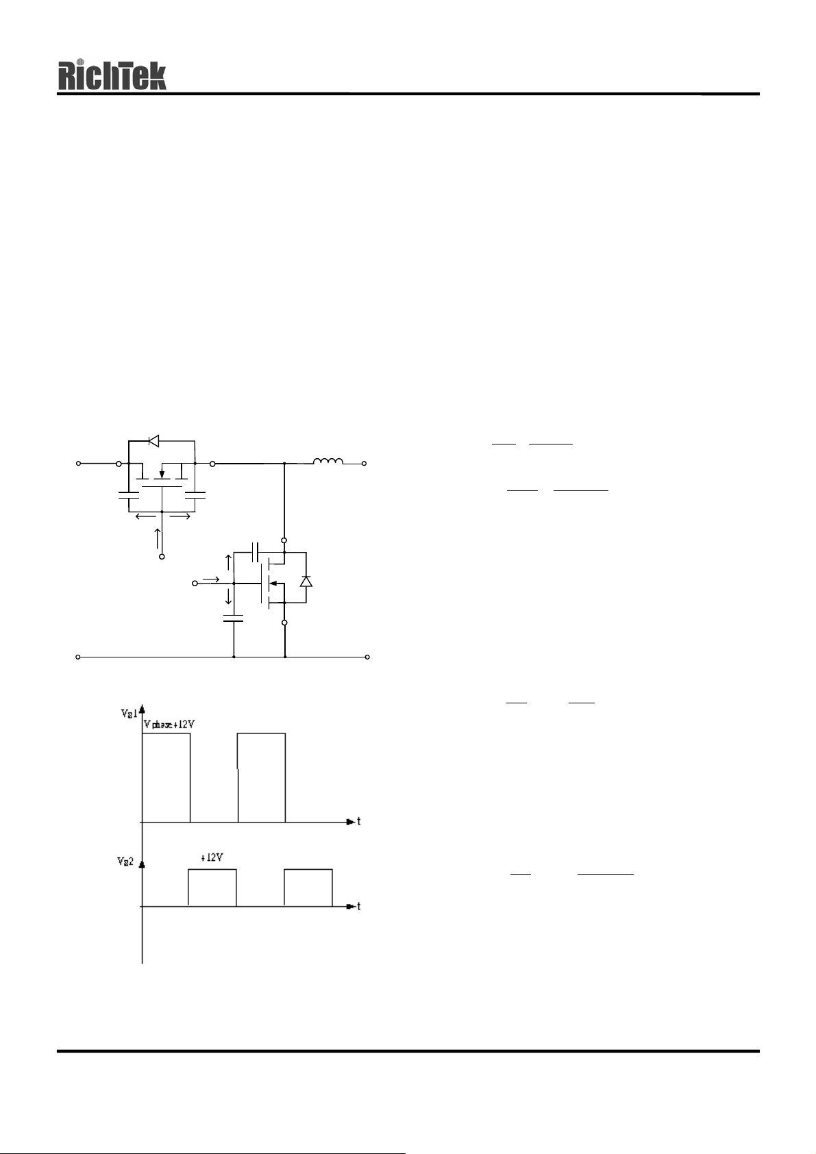
However, the capacitance at the gate to source
terminal should be considered. It requires relatively
large currents to drive the gate up and down 12V (or
5V) rapidly. It also required to switch drain current on
and off with the required speed. The required gate
drive currents are calculated as follows.
D1
d1
gd1 Cgs1
C
Igs1
Igd1
Ig1
g1
g2
at 12V (or 5V), the gate
gs
L
d2
D2
s2
Ig2
Cgs2
s1
Cgd2
Igd2
Igs2
VoVi
GND
In Figure 1, the current Ig1 and Ig2 are required to
move the gate up to 12V.The operation consists of
charging C
and Cgs. C
gd
and C
gs1
are the
gs2
capacitances from gate to source of the high side and
the low side power MOSFETs, respectively. In general
data sheets, the C
input capacitance. C
is referred as “C
gs
and C
gd1
gd2
” which is the
iss
are the capacitances
from gate to drain of the high side and the low side
power MOSFETs, respectively and referred to the data
sheets as “C
example, t
” the reverse transfer capacitance. For
rss,
and tr2 are the rising time of the high side
r1
and the low side power MOSFETs respectively, the
required current I
gs1
and I
are showed below
gs2,
dV
CI
gs1gs1
dt
dV
CI
gs2gs2
dt
12C
×
gs1g1
==
(1)
t
r1
12C
×
gs1g2
==
(2)
t
r2
According to the design of RT9602, before driving the
gate of the high side MOSFET up to 12V (or 5V), the
low side MOSFET has to be off; and the high side
MOSFET is turned off before the low side is turned on.
From Figure 1, the body diode “D
” had been turned
2
on before high side MOSFETs turned on
dV
CI ==
dt
12V
C
gd1gd1gd1
(3)
t
r1
Before the low side MOSFET is turned on, the C
have been charged to Vi. Thus, as C
polarity and g
is charged up to 12V, the required
2
reverses its
gd2
gd2
current is
dV
dt
C
==
gd2gd2gd2
CI
12VVi
+
(4)
t
r2
Figure 1. The gate driver must supply Igs to Cgs and Igd to C
gd
DS9602-02 November 2002 www.richtek.com
7
Page 8
RT9602
It is helpful to calculate these currents in a typical case.
Assume a synchronous rectified BUCK converter, input
voltage V
MOSFET is PHB83N03LT whose C
380pF,and t
PHB95N03LT whose C
t
= 30nS, from the equation (1) and (2) we can obtain
r
= 12V, Vg1 = Vg2 = 12V. The high side
i
= 1660pF, C
iss
= 14nS. The low side MOSFET is
r
= 2200pF, C
iss
= 500pF, and
rss
rss
=
12
××
12101660
1.428(A) (5)
=
I
1gs
×
1014
=
−−9
12
××
12102200
=
I
2gs
−−9
×
1030
0.88(A) (6)
=
from equation. (3) and (4)
12
××
1210380
0.326(A) (7)
=
I
gd1
×
1014
=
−−9
12
I
=
2gd
−−9
1030
×
)1212(10500
+××
0.4(A) (8)
=
the total current required from the gate driving source
is
1.745(A) (9)
1gd1gs1g
=+=+= )326.0428.1(III
= 1.28(A) (10)
)4.088.0(III
2gd2gs2g
+=+=
By a similar calculation, we can also get the sink
current required from the turned off MOSFET.
Layout Consider
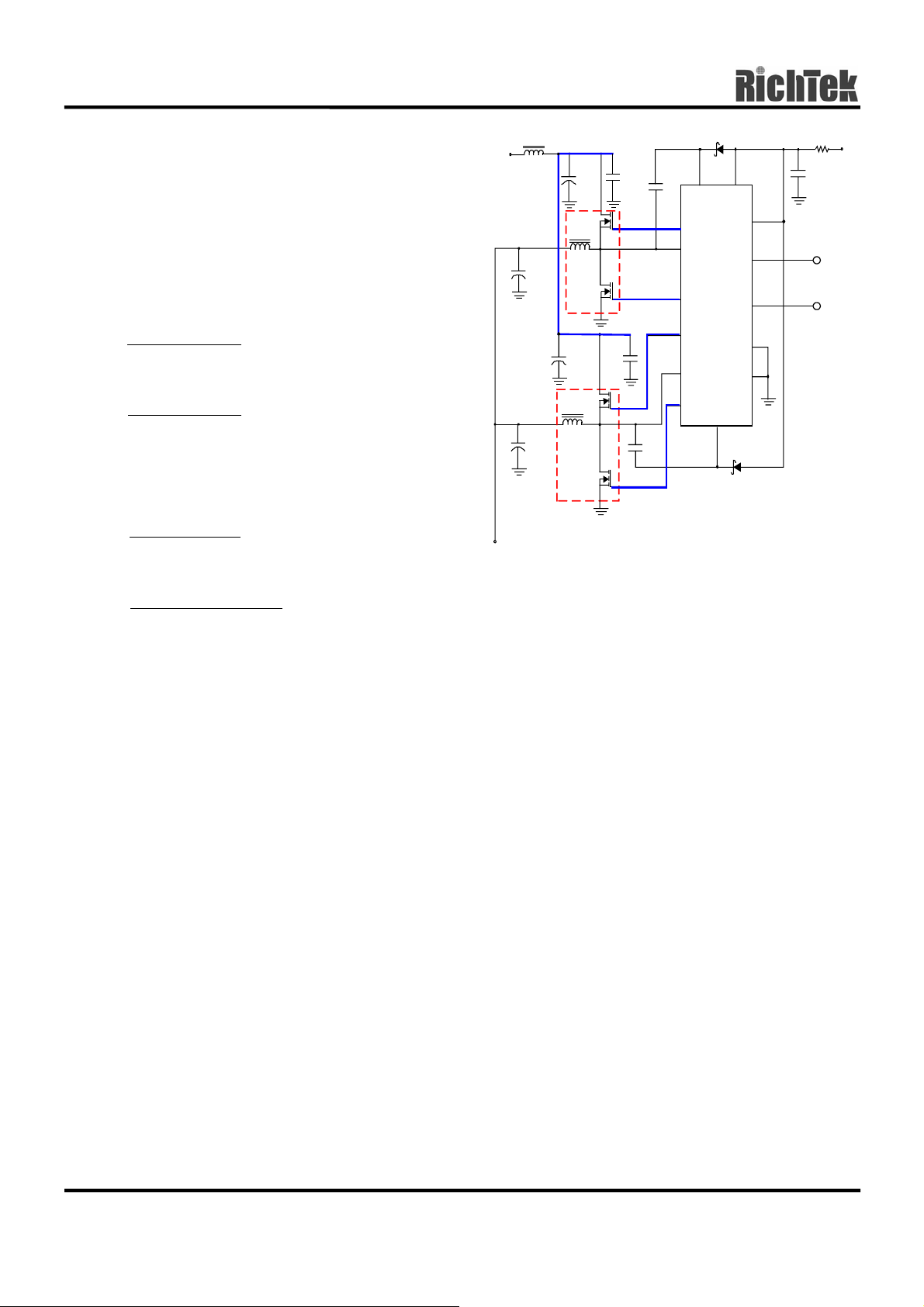
Figure 2. shows the schematic circuit of a two-phase
synchronous-buck converter to implement the RT9602.
The converter operates for the input rang from 5V to
12V.
V
Vin
12V
CORE
L1
uH
1.2
C1
1000uF
C5
1500uF
C3
1000uF
C6
1500uF
L3
2uH
L2
2uH
Q3
Q4
Q1
PHB83N03LT
Q2
PHB95N03LT
C4
1uF
PHB83N03LT
PHB95N03LT
C2
1uF
Cb2
1uF
Cb1
1
uF
12
13
4
9
8
7
11
BOOT1
UGATE1
PHASE1
RT9602
LGATE1
UGATE2
PHASE2
LGATE2
BOOT2
D1
VCC
PVCC
PWM1
PWM2
PGND
10
GND
D2
14
5
1
2
3
6
C7
1uF
R1
10Ω
12V
PWM1
PWM2
Figure 2. Two- Phase Synchronous-Buck Converter Circuit
When layout the PC board, it should be very careful.
The power-circuit section is the most critical one. If not
configured properly, it will generate a large amount of
EMI. The junction of Q1, Q2, L2 and Q3, Q4, L4 should
be very close. The connection from Q1, and Q3 drain
to positive sides of C1, C2, C3, and C4; the connection
from Q2, and Q4 source to the negative sides of C1,
C2, C3, and C4 should be as short as possible.
Next, the trace from Ugate1, Ugate2, Lgate1, and
Lgate2 should also be short to decrease the noise of
the driver output signals. Phase1 and phase2 signals
from the junction of the power MOSFET, carrying the
large gate drive current pulses, should be as heavy as
the gate drive trace. The bypass capacitor C7 should
be connected to PGND directly. Furthermore, the
bootstrap capacitors (C
, Cb2) should always be
b1
placed as close to the pins of the IC as possible.
www.richtek.com DS9602-02 November 2002
8
Page 9
RT9602
Select the Bootstrap Capacitor
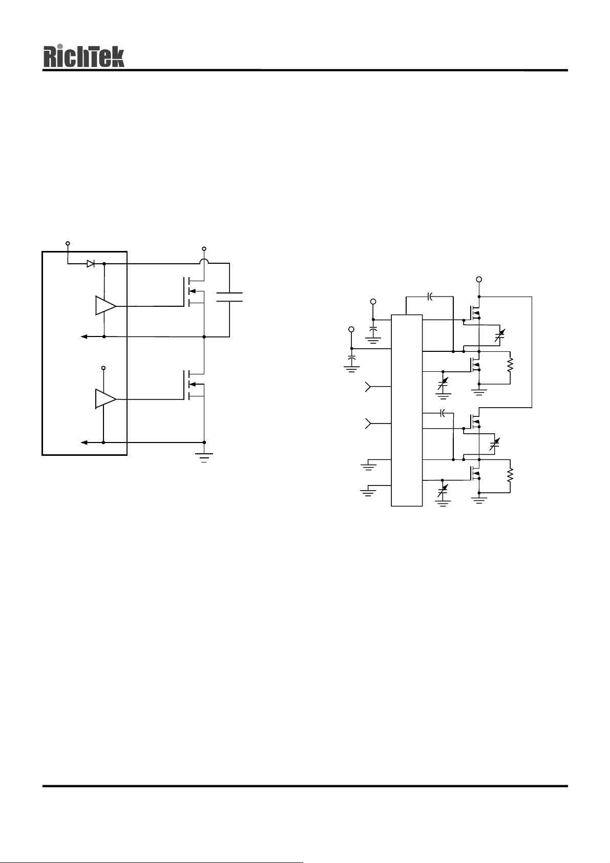
Figure 3. shows part of the bootstrap circuit of RT9602.
The V
(the voltage difference between BOOT1 and
CB
PHASE1 on RT9602) provides a voltage to the gate of
the high side power MOSFET. This supply needs to be
ensured that the MOSFET can be driven. For this, the
capacitance C
has to be selected properly. It is
B
determined by following constraints.
PVCC
BOOT1
UGATE1
PHASE1
PVCC
LGATE1
PGND
Vin
+
B
C
V
CB
-
Figure 3. Part of Bootstrap Circuit of RT9602
In practice, a low value capacitor C
will lead the
B
overcharging that could damage the IC. Therefore to
minimize the risk of overcharging and reducing the
ripple on V
, the bootstrap capacitor should not be
CB
smaller than 0.1µF, and the larger the better. In
general design, using 1µF can provide better
performance. At least one low-ESR capacitor should
be used to provide good local de-coupling. Here, to
adopt either a ceramic or tantalum capacitor is suitable.
Power Dissipation
For not exceeding the maximum allowable power
dissipation to drive the IC beyond the maximum
recommended operating junction temperature of 125°C,
it is necessary to calculate power dissipation
appropriately. This dissipation is a function of switching
frequency and total gate charge of the selected
MOSFET. Figure 4. shows the power dissipation test
circuit. C
and CU are the UGATE and LGATE load
L
capacitors, respectively. The bootstrap capacitor value
is 0.01µF.
+5V OR +12V
0.01 uF
+12V
1uF
1uF
PWM1
UGATE1
PHASE1
LGATE1 2N 7000
PWM2
PGND
GND
RT9602
UGATE2
PHASE2
LGATE2
0.01 uF
+5V OR +12V
C
L
C
L
2N7000
2N7000
2N7000
C
U
33Ω
C
U
Ω
33
Figure 4. RT9602 Power Dissipation Test Circuit
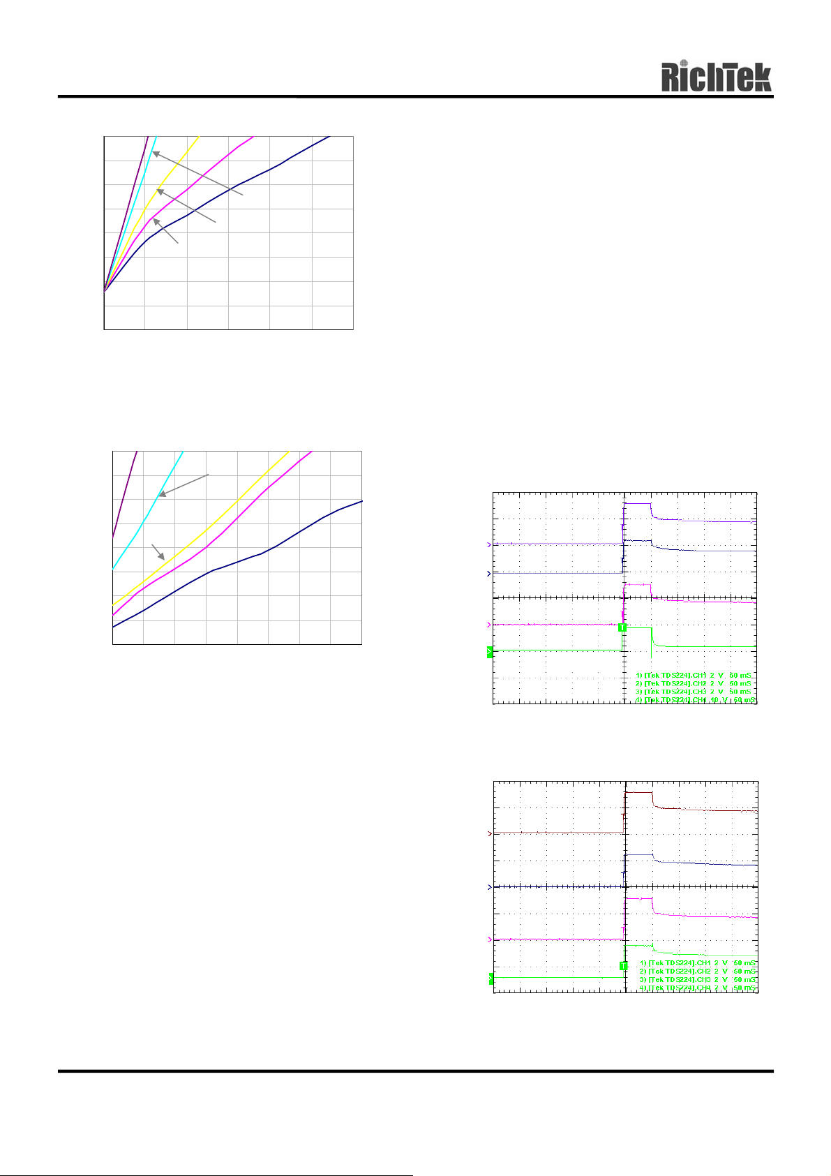
Figure 5. shows the power dissipation of the RT9602
as a function of frequency and load capacitance. The
value of the C
and CL are the same and the frequency
u
is varied from 100kHz to 600kHz. PVCC and VCC is
12V and connected together. Figure 6. shows the
same characterization for PVCC tied to 5V instead of
12V.
DS9602-02 November 2002 www.richtek.com
9
Page 10
RT9602
POWER (mW)
Power Dissipation vs. Frequency
800
C
U=CL
=5nF
700
600
500
400
300
C
200
100
0
U
0 100 200 300 400 500 600
C
= CL= 1nF
FREQUENCY (kHz)
= CL=2nF
U
C
= CL=3nF
U
C
= CL=4nF
U
PV
CC
= VCC = 12V
Figure 5. Power Dissipation vs. Frequency (RT9602)
POWER(mW)
Figure 6. Power Dissipation vs. Frequency, PVCC = 5V
Power Dissipation vs. Frequency
250
240
230
220
210
200
190
180
170
C
=5nF
C
50 100 150 200 250 300 350 400 450
U=CL
= CL=3nF
U
C
= CL=4nF
U
PV
CC
FREQUENCY(kHz)
= CL=2nF
C
U
= CL= 1nF
C
U
= 5V, VCC = 12V
The operating junction temperature can be calculated
from the power dissipation curves (Figure 5 and Figure
6). Assume the RT9602’s PVCC = VCC=12V,
operating frequency is 200kHz, and the C
U=CL
=1.5nF
which emulate the input capacitances of the high side
and low side power MOSFETs. From Figure 5, the
power dissipation is 500mW. In RT9602, the package
thermal resistance θ
is 127.67°C/W, the operating
JA
junction temperature is calculated as:
T
= 127.67°C/W × 500mW+ 25°C
J
= 88.84°C (11)
where the 25°C is the ambient temperature.
The method to improve the thermal transfer is to
increase the PC board copper area around the
RT9602, first. Then, adding a ground pad under IC to
transfer the heat to the peripheral of the board.
Power on Over-Voltage Protection Function
The RT9602 provides a protect function which can
avoid some short condition happened before power on.
The following discussion about the power on over-
voltage protection function of RT9602 is based on the
experiments of the high side MOSFET directly shorted
to 12V. The test circuit as shown in the typical
application circuit (with RT9241A/B dual-channel
synchronous-rectified buck controller) the VCC and the
phase signals are measured on the VCC pin and the
phase pin of RT9602. The LGATE signal is measured
on the gate terminal of MOSEFET.
V
CC
PHASE
LGATE
Current
Through
12V
10A/Div
Time (50mS)
Figure 7.. High Side Direct Short
V
CC
PHASE
LGATE
V
CORE
Figure 8. High Side Direct Short
Time (50mS)
www.richtek.com DS9602-02 November 2002
10
Page 11
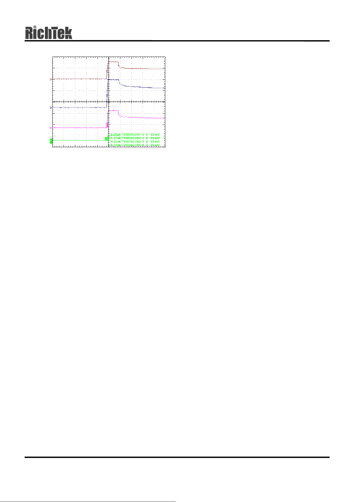
VCC
PHASE
LGATE
PWM1
RT9602
Time (25mS)
Figure 9. High Side Direct Short
Referring to Figure 7, when VCC exceeds 1.5V,
RT9602 turns on the LGATE to clamp the Phase
through the low side MOSFET. During the turn-on of
the low side MOSFET, the current of ATX 12V is limited
at 25A although the maximum current of ATX 12V
listed on the case of ATX is 15A. After the ATX 12V
shuts down, the VCC falls slowly. Please note that the
trigger point of RT9602 is at 1.5V VCC, and the
clamped value of phase is at about 2.4V. Next,
reference to Figure 8, it is obvious that since the Phase
voltage increases during the power-on, the V
CORE
increases correspondingly, but is gradually decreased
as LGATE and VCC decrease. In Figure 9, during the
turn-on of the low side MOSFET, the VCC is much less
than 12V, thus the RT9241A/B keeps the PWM signal
at high impedance state.
DS9602-02 November 2002 www.richtek.com
11
Page 12
RT9602
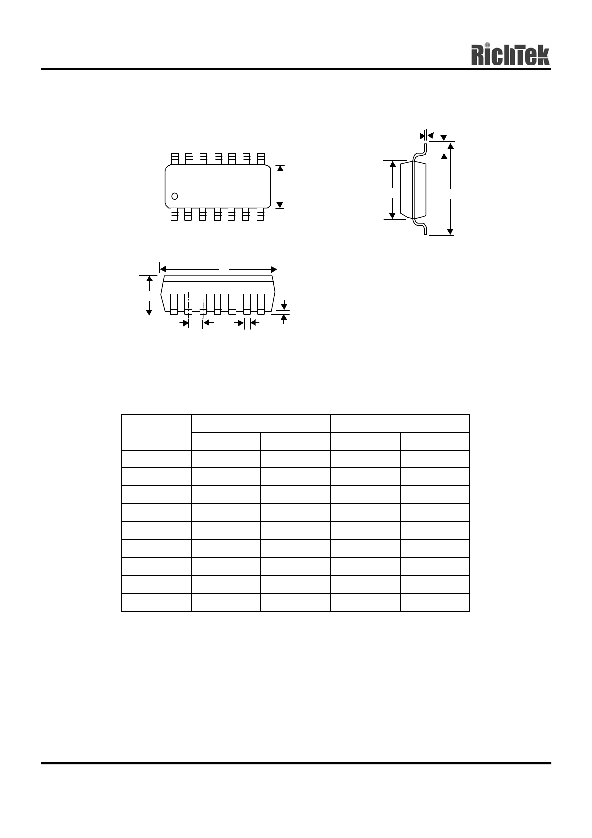
Package Information
H
M
B
A
C
F
D
I
B
J
Symbol
A 8.534 8.738 0.336 0.344
Dimensions In Millimeters Dimensions In Inches
Min Max Min Max
B 3.810 3.988 0.150 0.157
C 1.346 1.753 0.053 0.069
D 0.330 0.508 0.013 0.020
F 1.194 1.346 0.047 0.053
H 0.178 0.254 0.007 0.010
I 0.102 0.254 0.004 0.010
J 5.791 6.198 0.228 0.244
M 0.406 1.270 0.016 0.050
14–Lead SOP Plastic Package
www.richtek.com DS9602-02 November 2002
12
Page 13

RT9602
DS9602-02 November 2002 www.richtek.com
13
Page 14

RT9602
RICHTEK TECHNOLOGY CORP.
Headquarter
5F, No. 20, Taiyuen Street, Chupei City
Hsinchu, Taiwan, R.O.C.
Tel: (8863)5526789 Fax: (8863)5526611
RICHTEK TECHNOLOGY CORP.
Taipei Office (Marketing)
8F-1, No. 137, Lane 235, Paochiao Road, Hsintien City
Taipei County, Taiwan, R.O.C.
Tel: (8862)89191466 Fax: (8862)89191465
Email: [email protected]
www.richtek.com DS9602-02 November 2002
14
 Loading...