

Page 1
12V Synchronous Buck PWM DC/DC and
Linear Power Controller
RT9259
General Description
The RT9259 is a dual-channel DC/DC controller specifically
designed to deliver high quality power where 12V power
source is available. This part consists of a synchronous
buck controller and a n LDO controller. The synchronous
buck controller integrates MOSFET drivers that support
12V + 12V bootstra pped voltage for high efficiency power
conversion. The bootstra p diode is built-in to si mplify the
circuit design and minimize extern al part count. The LDO
controller drives an external N-MOSFET for lower power
requirement.
Other features include adjustable operation frequency,
internal soft start, under voltage protection, over current
protection and shut down function. With the above
functions, this part provides customers a compact, high
efficiency , well-protected and cost-ef f
ective solution. This
part comes to VQFN-16L 4x4, SOP14 and SSOP-16
packages.
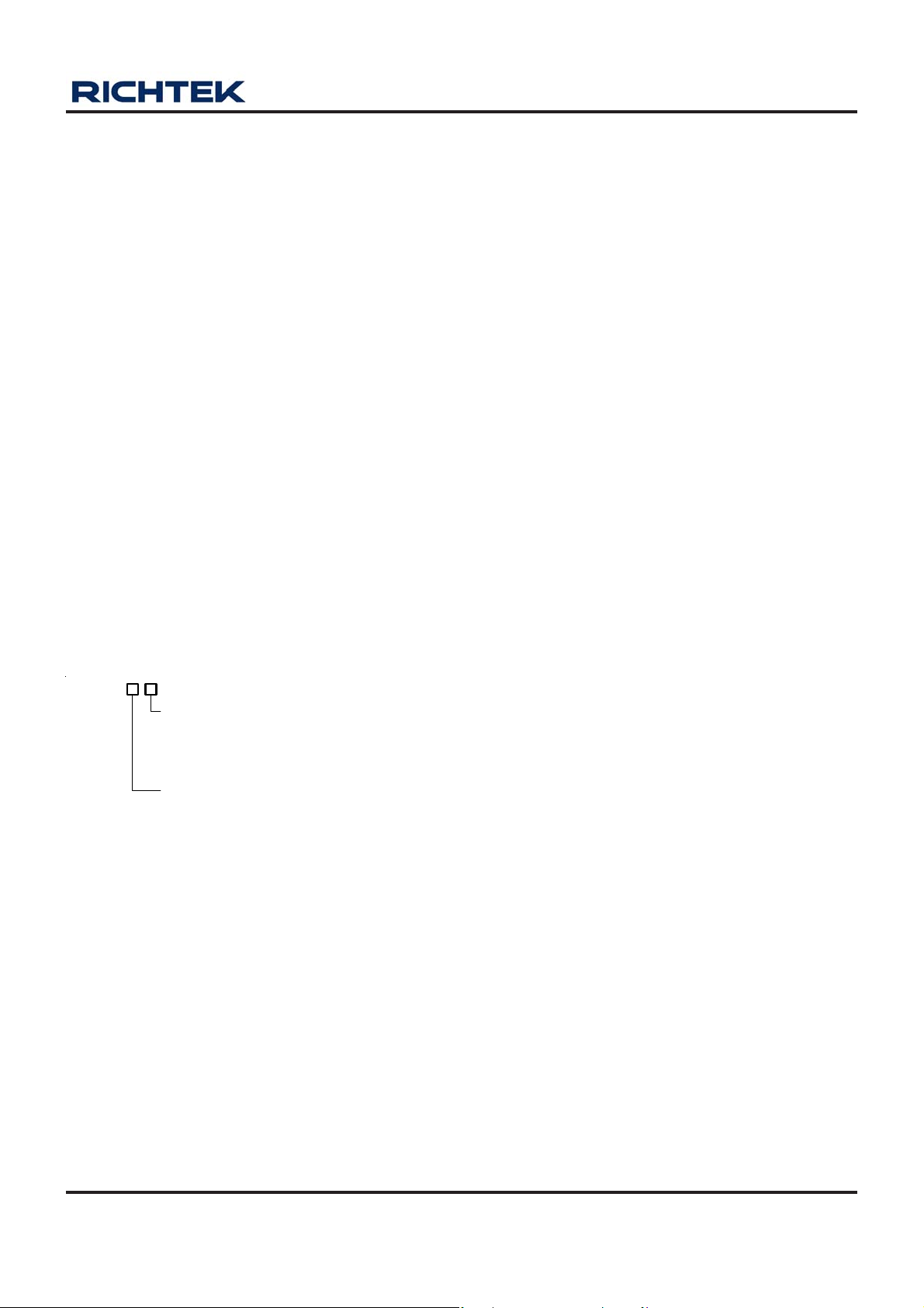
Ordering Information
RT9259
Package Type
S : SOP-14
A : SSOP-16
QV : VQFN-16 4x4 (V-Type)
Operating Temperature Range
P : Pb Free with Commercial Standard
G : Green (Halogen Free with Commer cial Standard)
Note :
Richtek Pb-free and Green products are :
` RoHS compliant and compatible with the current require-
ments of IPC/JEDEC J-STD-020.
` Suitable for use in SnPb or Pb-free soldering processes.
` 100% matte tin (Sn) plating.
Features
zz
Single 12V Bias Supply
z
zz
zz
z Support Dual Channel Power Conversion
zz
` One Synchronous Rectified Buck PWM Controller
` One Linear Controller
zz
z Both Controllers Drive Low Cost N-MOSFET s
zz
zz
z Adjustable Frequency from 150kHz to 1MHz
zz
and Free-Run Frequency at 230kHz
zz
z Small External Component Count
zz
zz
z Output Voltage Regulation
zz
`PWM Controller :
`LDO Controller :
zz
z Two Internal V
zz
zz
z Adjustable External Compensation
zz
zz
z Linear Controller Drive s N-MOSFET Pass
zz
±±
±1% Accuracy
±±
±±
±2% Accuracy
±±
Power Support Lower to 0.8V
REF
Transistor
zz
z Fully-Adjustable Outputs
zz
zz
z Under V oltage Prote ction for Both Outputs
zz
zz
z Over Current Fault Monitor on MOSFET; No Current
zz
Sense Resistor is Required
zz
z RoHS Compliant and 100% Lead (Pb)-Free
zz
Applications
z Graphic Card GPU, Memory Core Power
z Graphic Card Interfa ce Power
z Motherboard, Des ktop and Servers Chipset a nd Memory
Core Power
z IA Equipments
z T elecomm Equipments
z High Power DC-DC Regulators
Marking Information
For marking information, contact our sales re presentative
directly or through a Richtek distributor located in your
area, otherwise visit our website for detail.
DS9259-03T00 August 2007 www.richtek.com
1
Page 2
RT9259
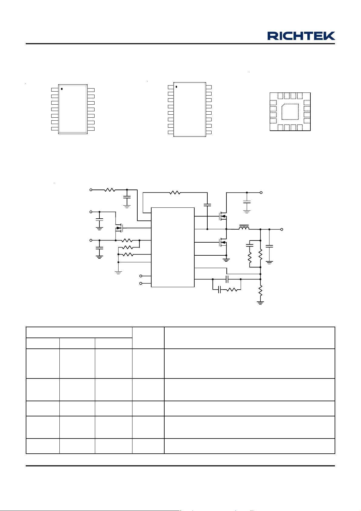
Pin Configurations
BOOT
FB
2
3
4
5
6
7
RT_DIS
COMP
DRV
FBL
GND
SOP-14
Typical Application Circuit
14
UGATE
13
PHASE
12
PGND
11
LGATE
10
NC
9
NC
VCC12
8
V
C
C
1
2
V
V
I
N
5
2
t
V
o
1
2
V
Q3
V
O
U
T
2
C
U
T
O
2
BOOT
RT_DIS
COMP
FB
DRV
FBL
GND
GND
BOOT
VCC12
DRV
FBL
RT_DIS
GND
NC
NC
(TOP VIEW)
2
3
4
5
6
7
8
SSOP-16
RT9259
UGATE
PHASE
LGATE
PGND
FB
COMP
16
15
14
13
12
11
10
UGATE
PHASE
PGND
LGATE
NC
NC
VCC12
VCC12
9
COMP
FB
DRV
FBL
RT_DIS
BOOT
PHASE
UGATE
13141516
PGND
NC
12
11
LGATE
10
17
NC
NC
9
8765
NC
VCC12
1
2
3
4
GND
VQFN-16L 4x4
V
N
I
1
V
/
3
3
.
5
1
V
2
/
V
C
IN
Q1
L
U
T
O
1
V
U
O
T
1
Q2
C
U
T
O
Functional Pin Description
Pin No.
Pin Name Pin Function
RT9259S RT9259A RT9259PQV
1 1 15 BOOT
2 2 16 RT_DIS
3 3 1 COMP
4 4 2 FB
5 5 3 DRV
2
Bootstrap supply for the upper gate driver. Connect the
bootstrap capacitor between BOOT pin and the PHASE pin.
The bootstrap capacitor provides the charge to turn on the
upper MOSFET.
Connect a resistor from RT_DIS to GND to set frequency. In
addition, if this pin is pulled do wn towards GN D, it will disab le
both regulator outputs until released.
Buck converter external compensation. This pin is used to
compensate the control loop of the buck converter.
Buck converter feedback voltage. This pin is the inverting input
of the PWM error amplifier. FB senses the switcher output
through an external resistor divider network.
Connect this pin to the gate of an ex ternal MOSFET. This pin
provides the drive for the linear regulator’s pass MOSFET.
To be continued
DS9259-03T00 August 2007www.richtek.com
Page 3
RT9259
Pin No.
Pin Name Pin Function
RT9259S RT9259A RT9259PQV
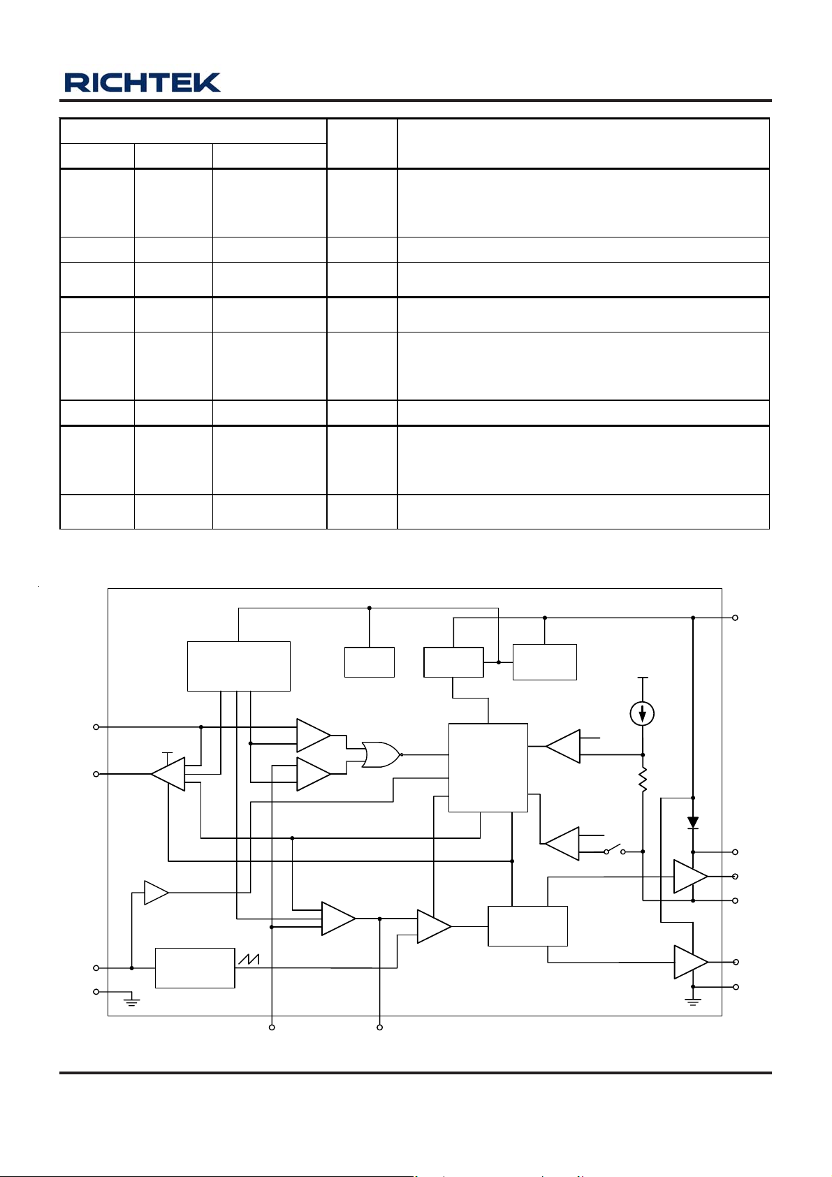
Linear regulator feedback voltage. This pin is the inverting
6 6 4 FBL
input of the LDO error amplifier and protection monitor.
Connect this pin to an external resistor divider network of
the linear re gulator .
7 7, 8 5 GND Ground.
8 9, 10 7 VCC12
9, 10 11, 12
6, 8, 9, 10,
17 (Expose d Pad)
NC No Internal Connection.
Connect this pin to a well-decoupled 12V bias supply. It is
also th e posit ive supply for the lower gate dr iver, LGATE.
Lower gate driver output. Connect to the gate of the
11 13 11 LGATE
low-side power N-MOSFET. This pin is monitored by the
adaptive shoot-through protection circuitry to determine
when the lower MOSFET has turned off.
12 14 12 PGND Power gro und re turn for th e lower gate dr iver .
Connect this pin to the source of the upper MOSFET and
13 15 13 PHASE
the drain of the lower MOS FET . Th is pi n is m oni to red by the
adaptive shoot-through protection circuitry to determine
when t he upper MOSF ET has tu rn ed off.
14 16 14 UGATE
Connect this pin to a well-decoupled 12V bias supply. It is
also th e posit ive supply for the lower gate dr iver, LGATE.
Function Block Diagram
Voltage
Reference
FBL
DRV
RT_DIS
GND
VCC12
Inhibit
V
REF2
+
+
Shutdown
Oscillator
V
0.4V
REF1
+
+
SSE
VCC12
Bias
+
+
EA
-
Power
On Reset
+
PWM
POR
Soft-Start
&
Fault Logic
SSE
5V
Regulator
OC
Driver
Logic
PH_M
5VDD
+
0.4V
-
-
1.5V
+
40uA
R
OCSET
20k
BOOT
UGATE
PHASE
LGATE
PGND
FB
COMP
DS9259-03T00 August 2007 www.richtek.com
3
Page 4

RT9259
Absolute Maximum Ratings (Note 1)
z Supply Voltage, V
z PHASE to GND
-------------------------------------------------------------------------------------- 15V
CC
DC------------------------------------------------------------------------------------------------------------- −5V to 15V
< 200ns------------------------------------------------------------------------------------------------------ −10V to 30V
z BOOT to PHASE ------------------------------------------------------------------------------------------15V
z BOOT to GND
DC------------------------------------------------------------------------------------------------------------- −0.3V to VCC+15V
< 200ns------------------------------------------------------------------------------------------------------ −0.3V to 42V
z UG ATE------------------------------------------------------------------------------------------------------- V
z LGATE ------------------------------------------------------------------------------------------------------- GND − 0.3V to V
z DRV ---------------------------------------------------------------------------------------------------------- GND − 0.3V to V
z Input, Output or I/O Voltage----------------------------------------------------------------------------- GND − 0.3V to 7V
z Power Dissipation, P
@ T
D
= 25°C
A
PHASE
− 0.3V to V
SOP-14 ------------------------------------------------------------------------------------------------------ 1.000W
SSOP-16 ---------------------------------------------------------------------------------------------------- 0.909W
VQFN-16L 4x4 --------------------------------------------------------------------------------------------- 1.852W
z Package Thermal Re sistance (Note 2)
SOP-14, θJA------------------------------------------------------------------------------------------------- 100°C/W
SSOP-16, θJA----------------------------------------------------------------------------------------------- 110°C/W
VQF N-16L 4x4, θJA---------------------------------------------------------------------------------------- 54°C/W
z Junction T emperature------------------------------------------------------------------------------------- 150°C
z Lead T e mperature (Soldering, 10 sec.)--------------------------------------------------------------- 260 °C
z Storage T emperature Range ---------------------------------------------------------------------------- −40°C to 150°C
z ESD Susceptibility (Note 3)
HBM (Human Body Mode) ------------------------------------------------------------------------------ 2kV
MM (Ma chine Mode)-------------------------------------------------------------------------------------- 200V
BOOT
+ 0.3V
CC
+ 0.3V
CC
+ 0.3V
Recommended Operating Conditions (Note 4)
z Supply Voltage, V
z Junction T emperature Range---------------------------------------------------------------------------- −40°C to 125°C
z Ambient T emperature Range---------------------------------------------------------------------------- −40°C to 85°C
-------------------------------------------------------------------------------------- 12V ± 10%
CC
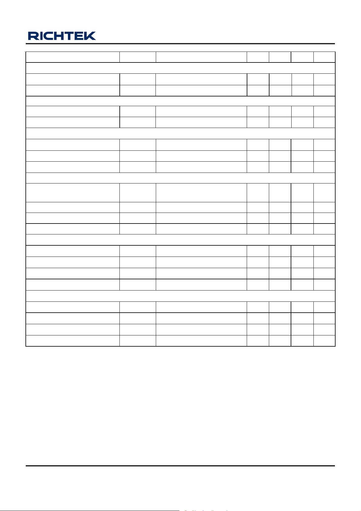
Electrical Characteristics
(VCC = 12V, T
Supply Input
Power Supply Voltage VCC -- 12 15 V
Power On Reset V
Power On Reset Hysteresis V
Power Supply Current I
4
= 25°C unless otherwise specified)
A
Parameter Symbol Test Conditions Min Typ Max Unit
VCCRTH
VCCHYS
VCC
VCC Rising 8.8 9.6 10.4 V
0.4 0.78 1.2 V
UGATE, LGATE Open -- 3 -- mA
To be continued
DS9259-03T00 August 2007www.richtek.com
Page 5
Oscillator
RT9259
Parameter Symbol Test Conditions Min Typ Max Unit
Free Running Frequency f
R
OSC
= 1 10k Ω 250 300 350 kHz
RT
Ramp Amplit ude -- 1.6 -- V
Reference Voltage
PWM Error Amplifier Reference V
Linear Driver Refe re nce V
0.792 0.8 0.808 V
REF1
0.784 0.8 0.816 V
REF2
Error Amplifier
DC Gain 70 88 - - dB
Gain-Bandwidth Product GBW
Slew Rate SR
C
LOAD
= 5pF
6 15 -- MHz
3 6 -- V/μs
Gate Driver
Upper Drive Sour ce R
Upper Drive Sink R
Lower Drive Source R
Lower Drive Sink R
UGATE
V
UGATE
VCC − V
LGATE
V
LGATE
V
BOOT
V
BOOT
UGATE
LGATE
− V
− V
= 1V -- 4 8 Ω
LGATE
= 1V -- 2 4 Ω
= 12V,
PHASE
UGATE
= 1V
-- 4 8 Ω
= 1V -- 4 6 Ω
Protection
Under Vol t age Prot ec tion
Soft-Start Time Interval
Over Current Thres hol d
V
T
V
UVP
SS
OC
0.36 0.4 0.45 V
2 3 4 ms
-- −400 -- mV
RT_DIS Shutdown Threshold 0.35 0.4 -- V
Linear Regulat or
Output High Vol tage
Output Low Voltage
Sour ce Cu rrent
Sink Current I
Note 1. Stresses listed as the above "Absolute Maximum Ratings" may cause permanent damage to the device. These are for
stress ratings. Functional operation of the device at these or any other conditions beyond those indicated in the
operational sections of the specifications is not implied. Exposure to absolute maximum rating conditions for extended
periods may remain possibility to affect device reliability.
Note 2. θ
Note 3. Devices are ESD sensitive. Handling precaution recommended.
Note 4. The device is not guaranteed to function outside its operating conditions.
DS9259-03T00 August 2007 www.richtek.com
is measured in the natural convection at TA = 25°C on a high effective 4-layers 2S2P thermal conductivity test board
JA
of JEDEC 51-7 thermal measurement standard.
V
DRV
V
DRV
I
DRVSR
DRVSC
0.5 -- -- mA
9.5 10.3 -- V
-- 0.1 1 V
2 -- -- mA
5
Page 6
RT9259
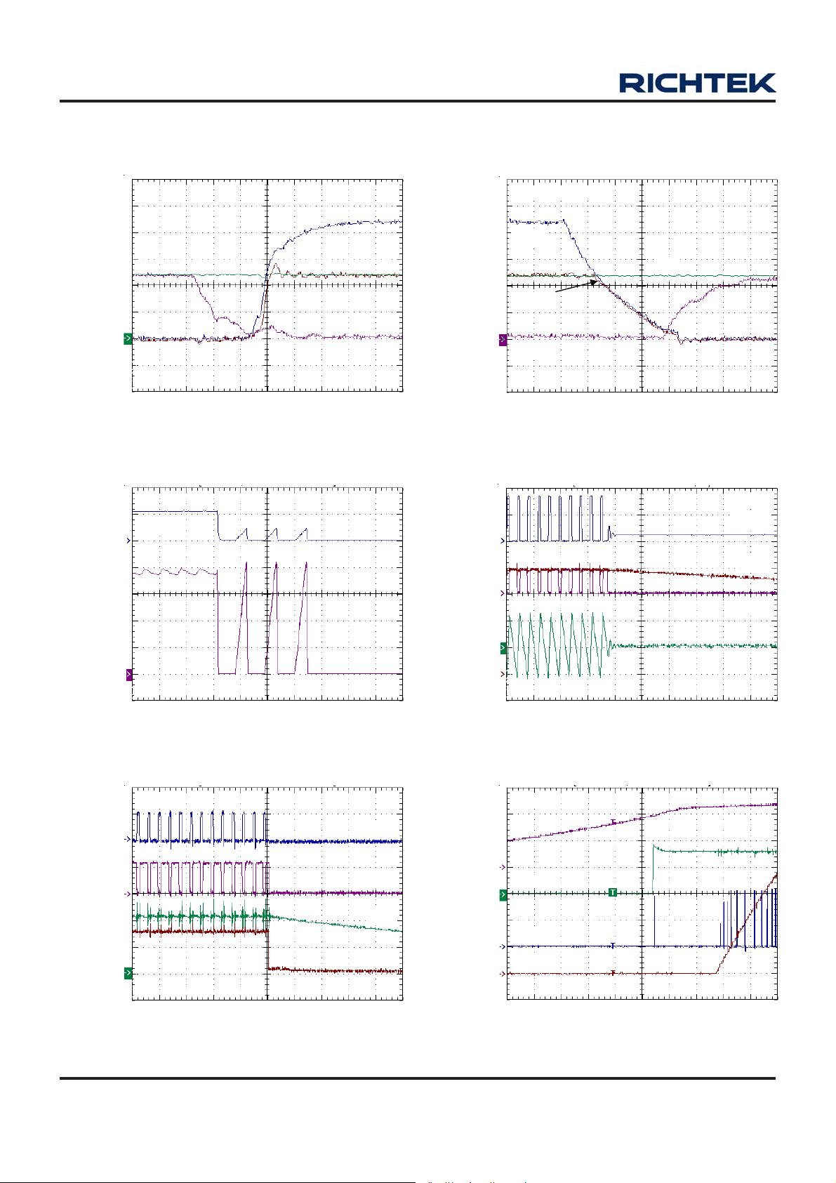
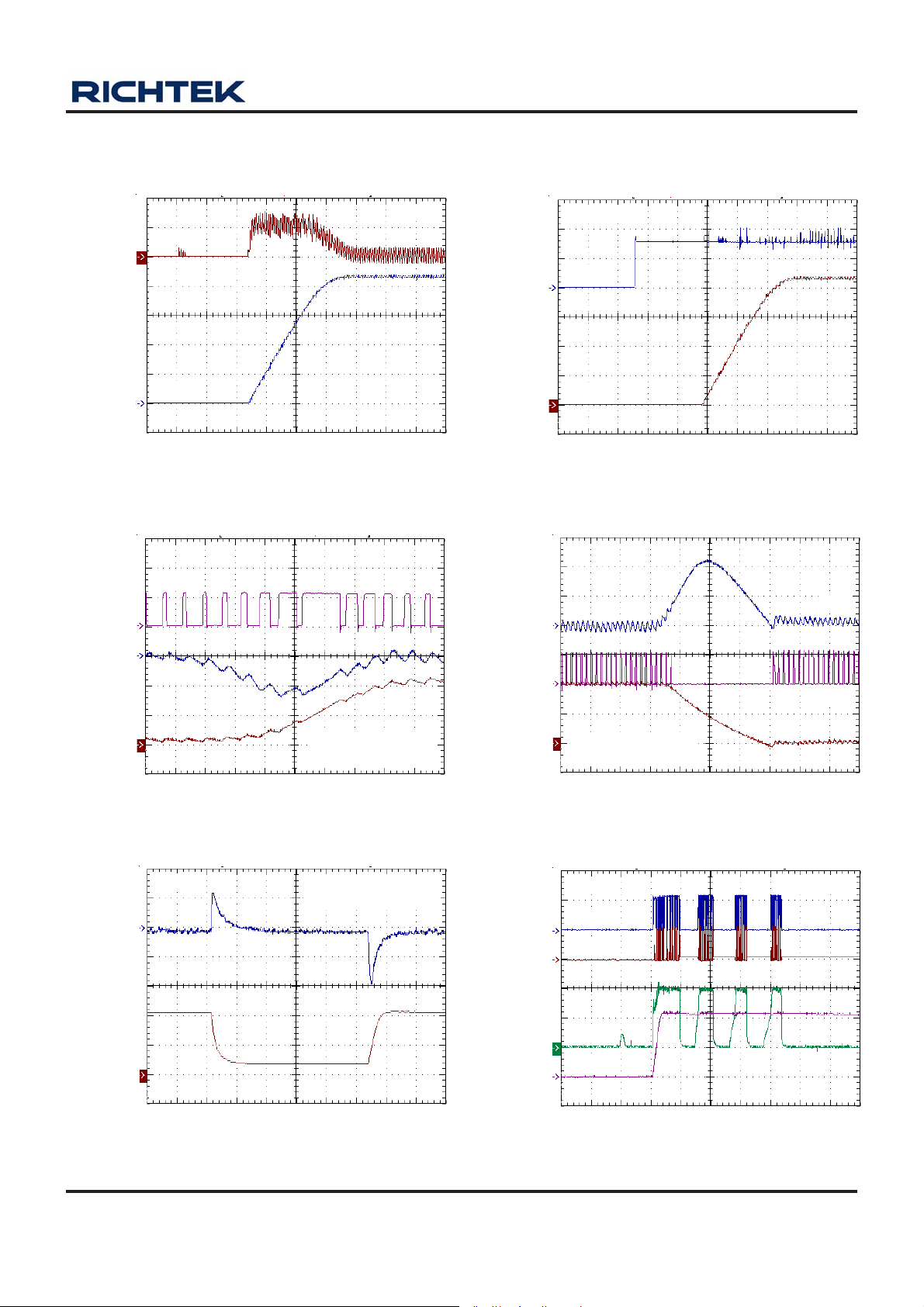
Typical Operating Characteristics
(5V/Div)
(2V/Div)
No Load, Falling
V
OUT1
I
L
Dead Time
V
IN1
PHASE
Time (25ns/Div)
OCP
UGATE
LGATE
(5V/Div)
(10V/Div)
(10V/Div)
No Load, Rising
UGATE
PHASE
LGATE
Dead Time
V
IN1
Time (25ns/Div)
Power Off
No Load
UGATE
V
REF
LGATE
(10A/Div)
(20V/Div)
(10V/Div)
(500mV/Div)
(1V/Div)
Full Load
Time (2.5ms/Div)
Shut Down
Time (5μs/Div)
UGATE
LGATE
V
OUT1
RT_Dis
(0.5A/Div)
(200mV/Div)
(5V/Div)
(500mV/Div)
(10V/Div)
(500mV/Div)
No Load
V
IN1
RT_Dis
PHASE
V
OUT1
Time (5μs/Div)
Start Up
Time (1ms/Div)
I
L
DS9259-03T00 August 2007www.richtek.com
6
Page 7
RT9259
(2.5A/Div)
(500mV/Div)
(20V/Div)
I
LOAD
V
OUT1
UGATE
Start Up
Time (1ms/Div)
Transient Response
No Load
(500mV/Div)
(500mV/Div)
(100mV/Div)
I
LOAD
RT_Dis
V
OUT1
Start Up
= 20A
Time (1ms/Div)
Transient Response
V
OUT
(100mV/Div)
(10A/Div)
(2mV/Div)
(0.5A/Div)
V
OUT1
I
L
LDO
V
I
L
OUT2
V
= 12V, V
IN1
I
= 1A to 20A
LOAD
Time (2.5μs/Div)
Transient Response
V
= 12V, V
IN2
I
= 1A to 100mA
LOAD
OUT1
OUT2
= 2V
= 2.5V
(20V/Div)
(10A/Div)
(10V/Div)
(20V/Div)
(500mV/Div)
(1V/Div)
V
IN1
I
LOAD
= 12V, V
= 20A to 1A
OUT1
= 2V
Time (10μs/Div)
Under Voltage Protection
LDO
LGATE
UGATE
COMP
V
OUT2
UGATE
V
IN2
= 0V
I
L
Time (100μs/Div)
Time (10ms/Div)
DS9259-03T00 August 2007 www.richtek.com
7
Page 8
RT9259
Application Information
Introduction
The RT9259 is a dual-channel DC/DC controller specifically
designed to deliver high quality power where 12V power
source is available. This part consists of a synchronous
buck controller and a n LDO controller. The synchronous
buck controller integrates internal MOSFET drivers that
support 12V+12V bootstra pped voltage for high efficiency
power conversion. The bootstra p diode is built-in to simplify
the circuit design and minimize external part count. The
LDO controller drives an external N-MOSFET for lower
power requirement.
Internal 5VDD Regulator
It is highly recommended to power the RT9259 with welldecoupled 12V to VCC12 pin. VCC12 powers the RT9259
control circuit, low side gate driver and bootstra p circuit for
high side gate driver. A bootstrap diode is embedded to
facilitates PCB design a nd reduce the total BOM cost. No
external Schottky diode is required. The RT9259 integrates
MOSFET gate drives that are powered from the VCC12
pin and support 12V + 12V driving capability. Converters
that consist of RT9259 feature high efficiency without
special consideration on the selection of MOSFETs.
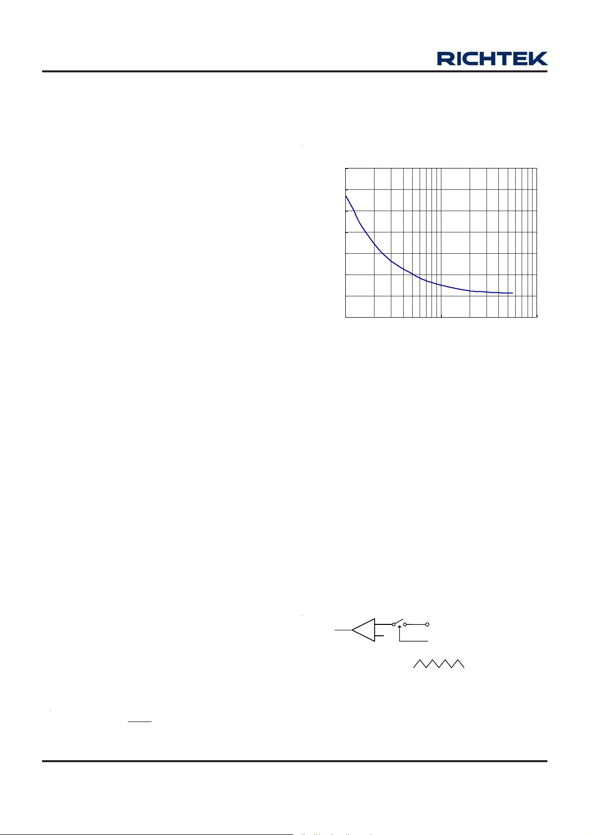
When let open, the free running frequency is 230kHz
typically . Figure 1 shows the operation frequency vs. R
RT
for quick reference.
1400
1200
1000
800
(kHz)
600
SW
f
400
200
0
10 100 1000
(kΩ)
RRT (kohm)
Figure 1. RT vs. fsw at Low Frequency
Shorting the RT_DIS pin to G ND with an extern al signallevel MOSFET shuts down the device. This allows flexible
power sequence control for specified application. The
RT_DIS pin threshold voltage is 0.4V typically.
An internal linear regulator regulates VCC12 input to a
5V DD voltage for internal control logic circuit. No external
bypass ca pa citor is required for filtering the 5V DD voltage.
This further facilitates PCB design and reduces the total
BOM cost.
Power On Reset
The RT9259 automatically initializes upon a pplying input
power (at the VCC12) pin. The power on reset function
(POR) continually monitors the input bias supply voltage
at the VCC12 pin. The VCC12V POR level is typically
9.6V at VCC12V rising.
Frequency Setting and Shut Down
Connecting a resistor RRT from the RT_DIS pin to GND
sets the operation frequency . The relation can be roughly
expressed in the equation.
7700
OSC
kHz302f
+≅
(kHz)
R
RT
VIN1 Detection
The RT9259 continuously generates a 10kHz pulse train
with 1μs pulse width to turn on the upper MOSFET for
detecting the existence of VIN1 after VCC12V POR and
RT_DIS enabled a s shown in Figure 2. PHASE pin voltage
is monitored during the detection duration.
If the PHASE voltage crosses 1.5V four times, VIN1
existence is recognized and the RT9259 initiates its soft
start cycle as described in next section.
V
POR_H
IN1
PHASE_M
+
-
1.5V
PHASE
UGATE
1st 2nd 3rd4th
Internal Counter will count (V
four times (rising & falling) to recognize
V
is ready.
IN1
PHASE
waveform
PHASE
> 1.5V)
Figure 2
DS9259-03T00 August 2007www.richtek.com
8
Page 9
RT9259
μ
Soft Start for Synchronous Buck Converter
A built-in soft-start is used to prevent surge current from
power supply input during power on (referring to the
Functional Block Di agram). The error a mplifier EA is a threeinput device. SSE or V
whichever is smaller dominates
REF1
the behavior non-inverting input. The internal soft start
voltage SSE linearly ramps up to about 4V after VIN1
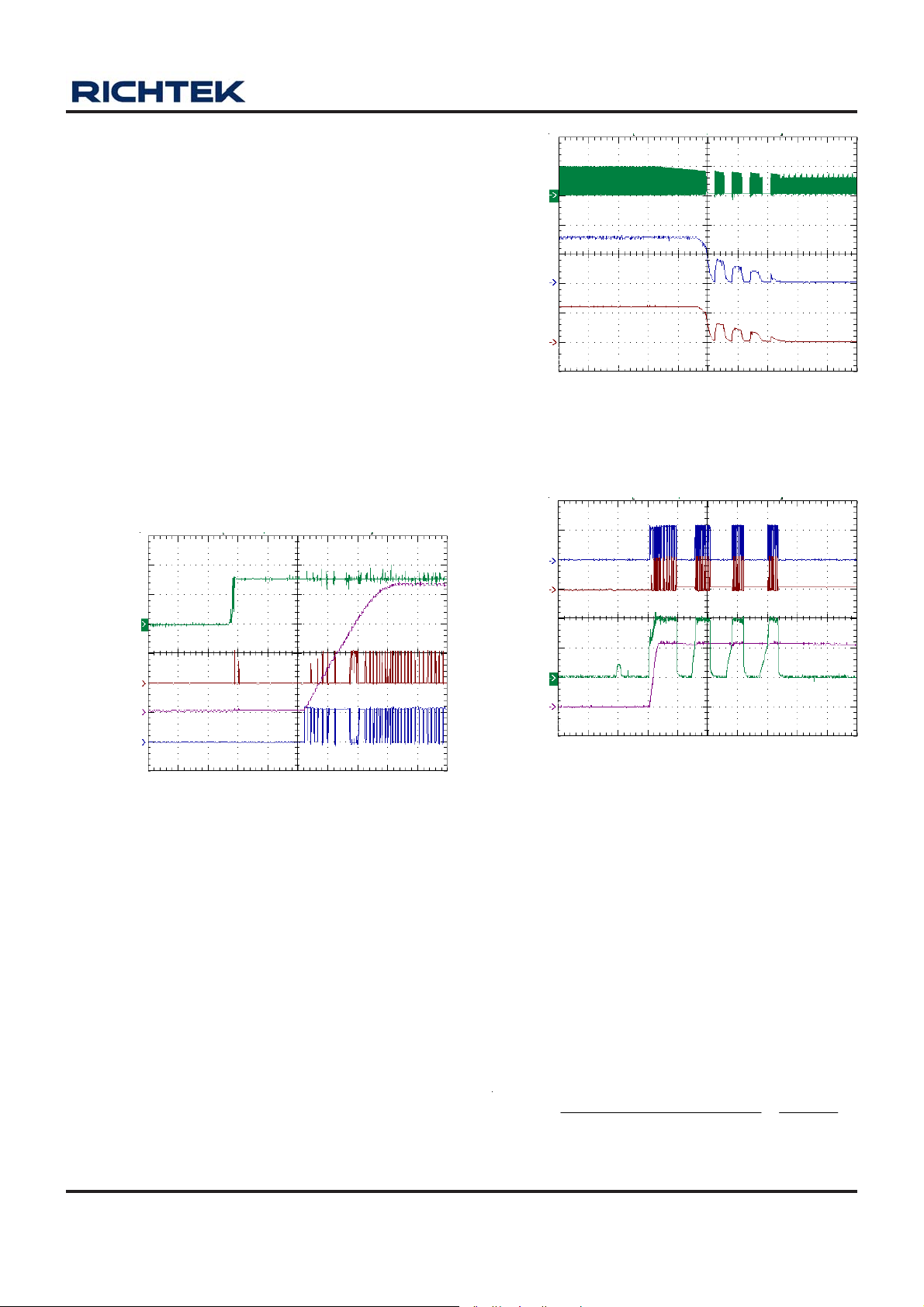
existence is recognized with about 2ms delay . According,
the output voltage ramps up smoothly to its target level.
The rise time of output voltage is about 2ms as shown in
Figure 3. V
V
.
REF1
takes over the behavior EA when SSE >
REF1
SSE is also used for LDO soft start. LDO input voltage
VIN2 MUST be ready before SSE starts to ramp up.
Otherwise UVP function of LDO may be triggered and shut
down the RT9259.
RT_DIS
(500mV/Div)
UGATE
(20V/Div)
FB
(500mV/Div)
V
OUT
(20V/Div)
LGATE
(10V/Div)
UGATE
(20V/Div)
V
Time (10ms/Div)
Figure 4. UVP triggered by FB
= 12V to 0V
IN1
V
IN2
= 0V
UGATE
(20V/Div)
V
OUT1
(500mV/Div)
LGATE
(10V/Div)
Time (1ms/Div)
Figure 3 : Start up by RT_DIS
Under Voltage Protection
The voltages at FB and FBL pin are monitored for under
voltage protection (UVP) after the soft start is completed.
UVP is triggered if one of the feedba ck voltages is under
(50% x V
) with a 30us delay. As shown in Figure 4,
REFX
the RT9259 PWM controller is shut down when VFB drops
lower than the UVP threshold. In Figure 5, the RT9259
shuts down after 4 time UVP hiccups triggered by FBL.
COMP
(500mV/Div)
V
OUT1
(1V/Div)
Time (10ms/Div)
Figure 5. UVP hiccups triggered by FBL
Over Current Protection
The RT9259 senses the current flowing through lower
MOSFET for over current protection (OCP) by sensing the
PHASE pin voltage as shown in the Functional Block
Diagra m. A 40μA current source flows through internal 20kΩ
R
to PHASE pin causes 0.8V voltage drop across
OCSET
the resistor. OCP is triggered if the voltage at PHASE pin
(drop of lower MOSFET VDS) is lower than −0.4V when low
side MOSFET conducting. Accordingly inductor current
threshold for OCP is a function of conducting resistance
of lower MOSFET R
I =
OCSET
=
DS(ON)
OCSET
R
as :
0.4V-)(20kRA40
Ω×
R
0.4V
DS(ON)DS(ON)
DS9259-03T00 August 2007 www.richtek.com
9
Page 10
RT9259
If MOSFET with R
= 16mΩ is used, the OCP
DS(ON)
threshold current is about 25A. Once OCP is triggered,
the RT9259 enters hiccup mode and re-soft starts again.
The RT9259 shuts down after 4 time OCP hiccups.
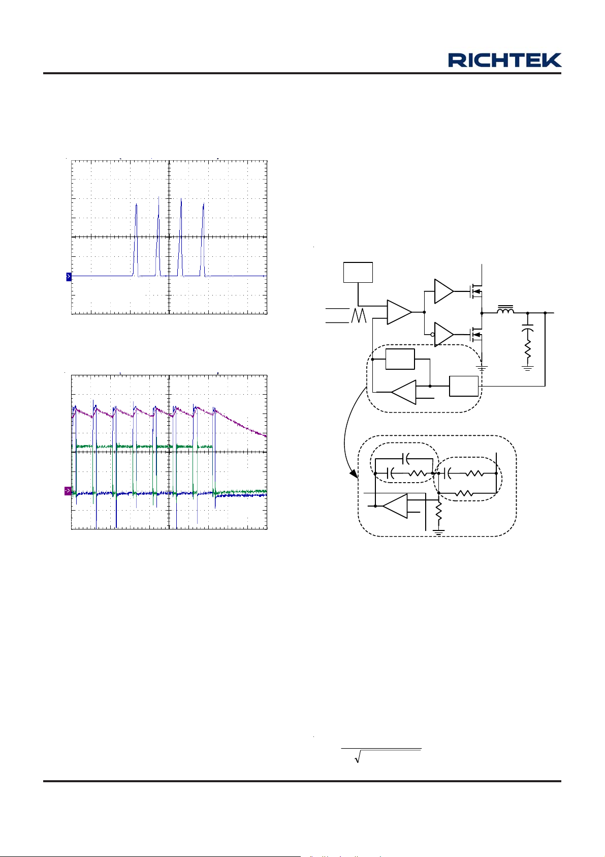
Inductor Current
(20A/Div)
Time (2.5ms/Div)
Figure 6. Shorted then Start Up
I
L
(20A/Div)
A well-designed compensator regulates the output voltage
to the reference voltage V
with fast tra nsient response
REF
and good stability.
In order to achieve fast transient response and accurate
output regulation, an adequate compensator design is
necessary. The goal of the compensation network is to
provide adequate pha se margin (greater than 45 degrees)
and the highest 0dB crossing frequency. It is also
recommended to manipulate loop frequency respon se that
its gain crosses over 0dB at a slope of −20dB/dec.
V
IN
ΔV
OSC
OSC
Comparator
PWM
+
COMP
Z
FB
EA
Driver
L
Driver
+
REF
PHASE
C
Z
IN
OUT
ESR
V
OUT
LGATE
(5V/Div)
UGATE
(5V/Div)
Time (5μs/Div)
Figure 7. Shorted then Start Up (Extended Figure 3)
Feedback Compensation
The RT9259 is a voltage mode controller. The control loop
is a single voltage feedback path including a compensator
and modulator a s shown Figure 8. The modulator consists
of the PWM comparator and power stage. The PWM
comparator compares error amplif ier EA output (COMP)
with oscillator (OSC) sawtooth wave to provide a PulseWidth Modulated (PWM) with an amplitude of VIN at the
PHASE node. The PWM wave is smoothed by the output
filter L
OUT
and C
. The output voltage (V
OUT
) is sensed
OUT
and fed to the inverting input of the error a mplifier .
C1
COMP
EA
C2
+
R2
REF
FB
Z
FB
C3
R1
Z
R3
V
OUT
IN
Figure 8. Closed Loop
1) Modulator Frequency Equations
The modulator trans fer function is the small-signal trans fer
function of V
OUT/VCOMP
(output voltage over the error
a mplif ier output. This trans fer function is domin ated by a
DC gain, a double pole, and a zero a s shown in Figure 10.
The DC gain of the modulator is the input voltage (VIN)
divided by the peak to peak oscillator voltage V
OSC
. The
output LC filter introduces a double pole, 40dB/decade
gain slope above its corner resona nt frequency, a nd a total
phase lag of 180 degrees. The resona nt frequency of the
LC filter expressed a s :
f
=
LC
π
1
CL2
×
OUTOUT
10
DS9259-03T00 August 2007www.richtek.com
Page 11
RT9259
The ESR zero is contributed by the ESR associ ated with
the output capacitance. Note that this requires that the
output capa citor should have enough ESR to satisfy stability
requirements. The ESR zero of the output capacitor
expressed as f ollows :
f
ESR
=
π
1
OUT
ESRC2
××
2) Compensation Frequency Equations
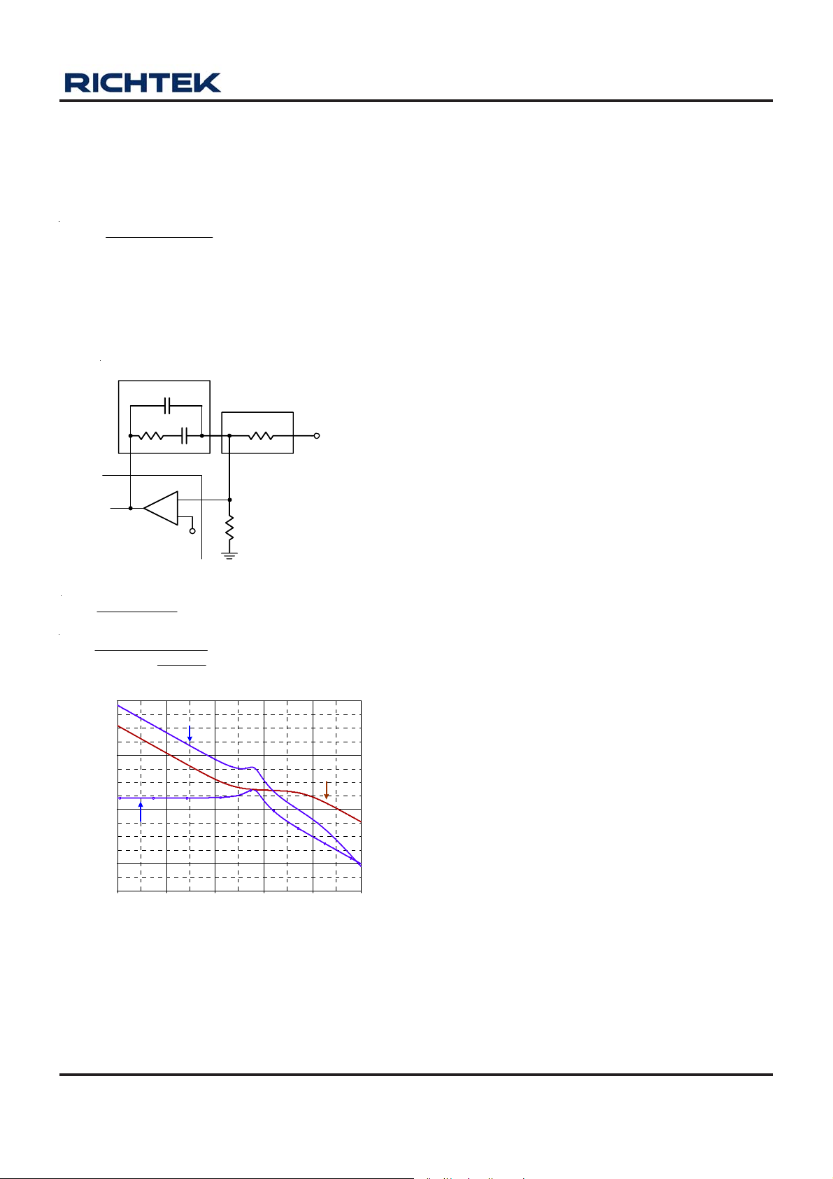
The compensation network consists of the error a mplifier
and the impedance networks ZC and ZF as shown in
Figure 9.
Z
F
C1
Z
C
C2
COMP
R2
EA
FB
+
V
REF
R1
R
F
V
OUT
Figure 9. Compensation Loop
=
f
Z1
f
=
P1
1
π
C2 x R2 x 2
1
x R2 x 2
π
80
80
60
40
40
20
0
0
Modulator
Gain (d B)
-20
Gain
-40
-40
-60
-60
10Hz 100Hz 1.0KHz 10KHz 100KHz 1.0MHz
10 100 1k 10k 100k 1M
vdb(vo) vdb(comp2) vdb(lo)
C2 x C1
C2C1
+
Loop Gain
Frequency
Frequency (Hz)
Compensation
Gain
Figure 10. Bode Plot
Figure 10 shows the DC-DC converter's gain vs. frequency .
The compensation gain uses external impeda nce networks
ZC and ZF to provide a stable, high bandwidth loop. High
crossover frequency is desirable for fa st transient respon se,
but often jeopardize the system stability . In order to cancel
one of the LC filter poles, place the zero before the LC
filter resona nt frequency. In the experience, pla ce the zero
at 75% LC filter resona nt frequency. Crossover frequency
should be higher than the ESR zero but less than 1/5 of
the switching frequency . The second pole is placed at hal f
the switching frequency .
Thermal Considerations
For continuous operation, do not exceed absolute
maximum operation junction temperature 125°C. The
maximum power dissipation depends on the thermal
resistance of IC package, PCB layout, the rate of
surroundings airflow and temperature difference between
junction to ambient. The maximum power dissipation ca n
be calculated by following formula :
P
Where T
temperature 125°C, T
θ
= ( T
D(MAX)
J(MAX)
is the junction to ambient thermal resistance.
JA
− TA ) / θ
J(MAX)
JA
is the maximum operation junction
is the ambient te mperature and the
A
For recommended operating conditions specification of
RT9259, where T
is the maximum junction
J(MAX)
temperature of the die (125°C) and TA is the maximum
ambient temperature. The junction to ambient thermal
resistance θJA is layout dependent. For VQFN-16L 4x4
packages, the thermal resistance θJA is 54°C/W on the
standard JEDEC 51-7 four-layers thermal test board.
The maximum power dissipation at TA = 25°C can be
calculated by following formula :
P
= ( 125°C − 25°C ) / 54°C/W = 1.852 W for
D(MAX)
QF N-16L 4x4 pa ckages
P
= ( 125°C − 25°C) / 100°C/W = 1.000 W for
D(MAX)
SOP-14 packages
P
= ( 125°C − 25°C ) / 110°C/W = 0.909 W for
D(MAX)
SSOP-16 packages
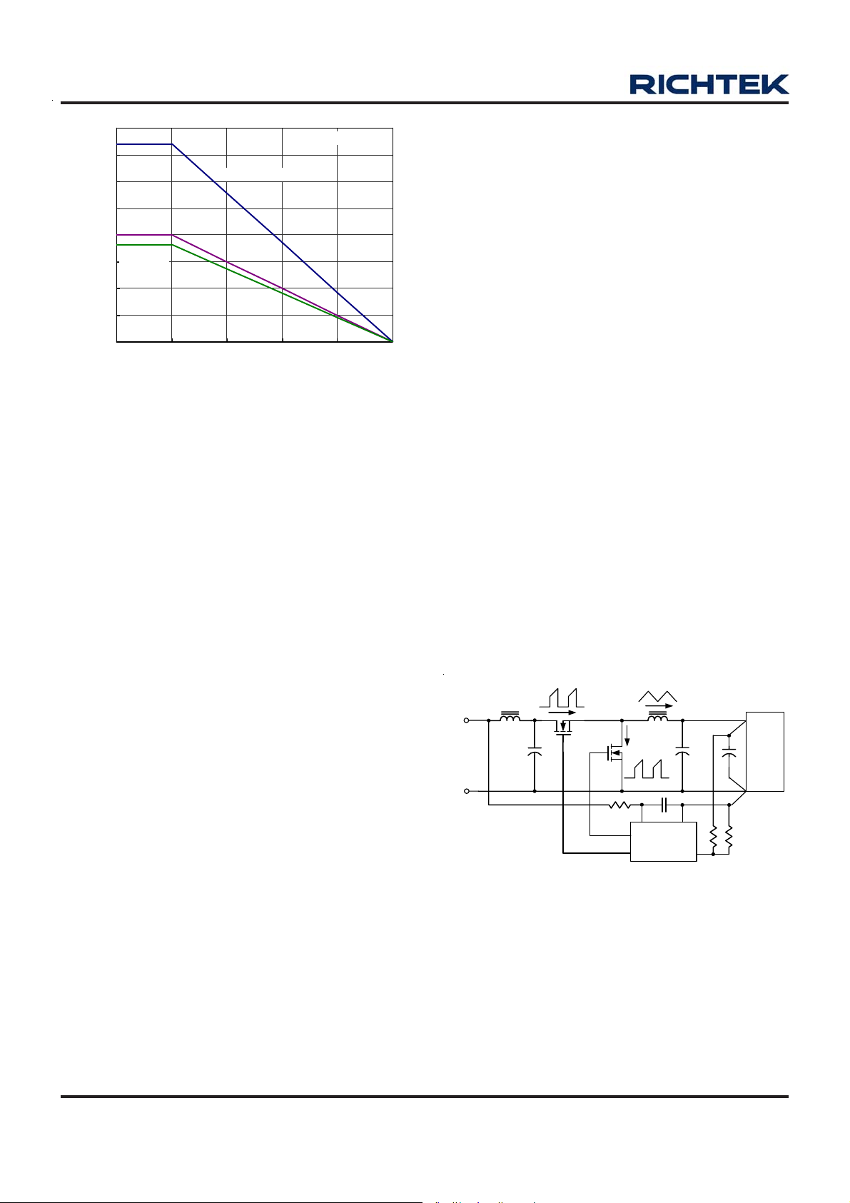
The maximum power dissipation depends on operating
a mbient temperature for fixed T
θ
. For RT9259 pack ages, the Figure 11 of derating curves
JA
and thermal resista nce
J (MAX)
allows the designer to see the effect of rising ambient
temperature on the maximum power allowed.
DS9259-03T00 August 2007 www.richtek.com
11
Page 12
RT9259
2
1.75
1.5
1.25
SOP-14
1
SSOP-16
0.75
0.5
0.25
Maximum Po wer Dissipati on (W)
0
0 25 50 75 100 125
QFN-16L 4x4
Ambient Temperature
4-Layers PCB
(°C)
Figure 11. Derating Curves for R T9259 Packages
PCB Layout Considerations
MOSFET s switch very fa st and ef ficiently . The speed with
which the current transitions from one device to another
causes voltage spikes across the interconnecting
impedances and parasitic circuit elements. The voltage
spikes can degrade eff iciency and radiate noise, that results
in over-voltage stress on devices. Careful component
placement layout a nd printed circuit design ca n minimize
the voltage spikes induced in the converter. Consider, a s
an example, the turn-off tran sition of the upper MOSFET
prior to turn-off, the upper MOSFET was carrying the full
load current. During turn-off, current stops flowing in the
upper MOSFET and is picked up by the low side MOSFET
or schottky diode.
Any inductance in the switched current path generates a
large voltage spike during the switching interval. Careful
component selections, layout of the critical components,
and use shorter a nd wider PCB tra ces help in minimizing
the magnitude of voltage spikes.
The power components and the PWM controller should
be placed firstly . Pla ce the input ca pacitors, especi ally the
high-frequency ceramic de coupling capa citors, close to the
power switches. Place the output inductor and output
capa citors between the MOSFET s and the loa d. Also locate
the PWM controller near by MOSFET s. A multi-layer printed
circuit board is recommended. Figure 12 shows the
connections of the critical components in the converter.
Note that the capacitors CIN and C
each of them
OUT
represents numerous physical ca pa citors.
Use a dedicated grounding plane a nd use vias to ground
all critical components to this layer. Apply another solid
layer as a power pla ne and cut this plane into smaller isla nds
of common voltage levels. The power plane should support
the input power and output power nodes. Use copper filled
polygons on the top and bottom circuit layers for the PHASE
node, but it is not necessary to oversize this particular
island. Since the PHASE node is subjected to very high
dV/dt voltages, the stray capacitance formed between
these islands a nd the surrounding circuitry will tend to couple
switching noise. Use the remaining printed circuit layers
for small signal routing. The PCB tra ces between the PWM
controller and the gate of MOSFET and also the traces
connecting source of MOSFETs should be sized to carry
2A pea k currents.
5V/12V
GND
IQ1
Q1
+
Q2
LGATE
UGATE
IQ2
VCC
IL
GND
RT9259
FB
V
OUT
+
+
LOAD
There are two sets of critical components in a DC-DC
converter using the RT9259. The switching power
components are most critical because they switch large
amounts of energy, and as such, they tend to generate
equally large amounts of noise. The critical small signal
components are those connected to sensitive nodes or
those supplying critical bypass current.
12
Figure 12. The connections of the critical components in
the converter
DS9259-03T00 August 2007www.richtek.com
Page 13
Outline Dimension
RT9259
A
J
I
Dimensions In Millimeters Dimensions In Inches
Symbol
Min Max Min Max
A 8.534 8.738 0.336 0.344
B 3.810 3.988 0.150 0.157
B
F
C
D
H
M
C 1.346 1.753 0.053 0.069
D 0.330 0.508 0.013 0.020
F 1.194 1.346 0.047 0.053
H 0.178 0.254 0.007 0.010
I 0.102 0.254 0.004 0.010
J 5.791 6.198 0.228 0.244
M 0.406 1.270 0.016 0.050
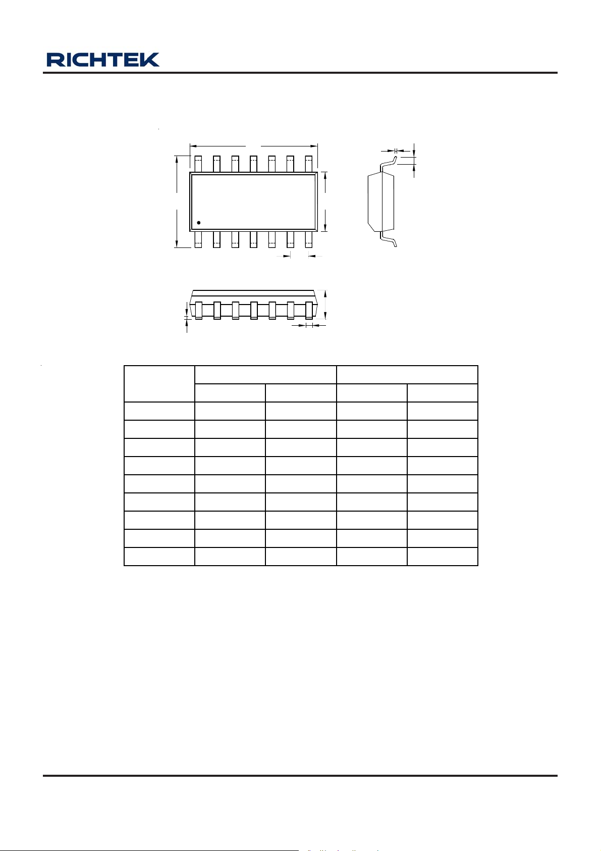
14–Lead SOP Plastic Package
DS9259-03T00 August 2007 www.richtek.com
13
Page 14
RT9259
c
D
L
E
A
b
Dimensions In Millimeters Dimensions In Inches
Symbol
Min Max Min Max
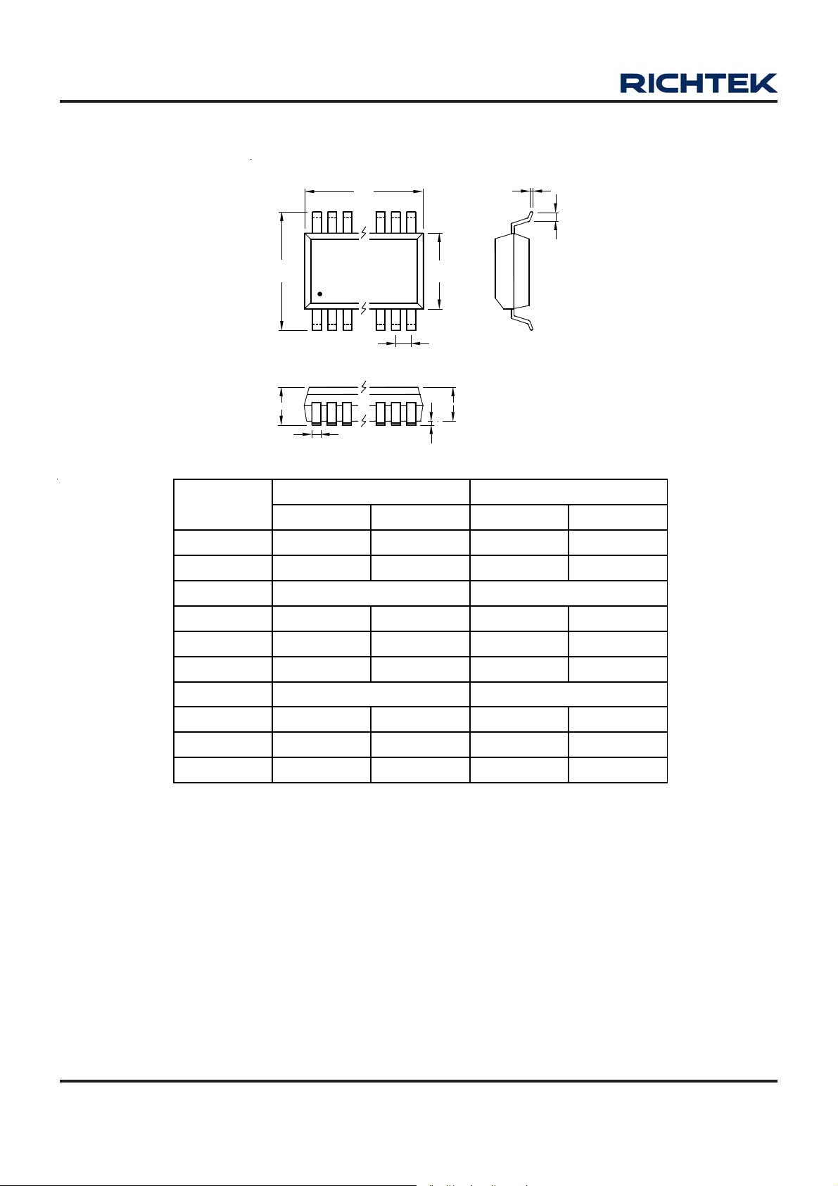
A 1.346 1.753 0.053 0.069
A1 0.102 0.254 0.004 0.010
A2 1.499 0.059
b 0.203 0.305 0.008 0.012
C 0.178 0.254 0.007 0.010
D 4.801 5.004 0.189 0.197
E1
e
A2
A1
14
e 0.635 0.025
E 5.791 6.198 0.228 0.244
E1 3.810 3.988 0.150 0.157
L 0.406 1.270 0.016 0.050
16-Lead SSOP Plastic Package
DS9259-03T00 August 2007www.richtek.com
Page 15
RT9259
D
D2
L
SEE DETAIL A
1
E
e
A
A3
A1
E2
1
b
2
1
2
DETAIL A
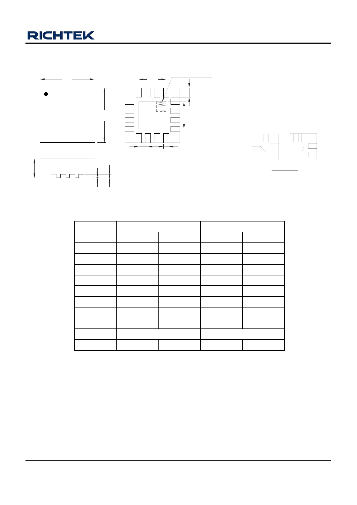
Pin #1 ID a nd T ie Bar Mark Option s
Note : The configuration of the Pin #1 identifier is optional,
but must be located within the zone indicated.
Dimensions In Millimeters Dimensions In Inches
Symbol
Min Max Min Max
A 0.800 1.000 0.031 0.039
A1 0.000 0.050 0.000 0.002
A3 0.175 0.250 0.007 0.010
b 0.250 0.380 0.010 0.015
D 3.950 4.050 0.156 0.159
D2 2.000 2.450 0.079 0.096
E 3.950 4.050 0.156 0.159
E2 2.000 2.450 0.079 0.096
e 0.650 0.026
L 0.500 0.600
Richtek Technology Corporation
Headquarter
5F, No. 20, Taiyuen Street, Chupei City
Hsinchu, Taiwan, R.O.C.
Tel: (8863)5526789 Fax: (8863)5526611
0.020 0.024
V-Type 16L QFN 4x4 Package
Richtek Technology Corporation
Taipei Office (Marketing)
8F, No. 137, Lane 235, Paochiao Road, Hsintien City
Taipei County, Taiwan, R.O.C.
Tel: (8862)89191466 Fax: (8862)89191465
Email: [email protected]
Information that is provided by Richtek Technology Corporation is believed to be accurate and reliable. Richtek reserves the right to make any change in circuit design,
specification or other related things if necessary without notice at any time. No third party intellectual property infringement of the applications should be guaranteed
by users when integrating Richtek products into any application. No legal responsibility for any said applications is assumed by Richtek.
DS9259-03T00 August 2007 www.richtek.com
15
 Loading...