

Page 1
Preliminary
RT9248
Multi-Phase PWM Controller for CPU Core Power Supply
General Description
The RT9248 is a multi-phase buck DC/DC controller
integrated with all control functions for GHz CPU VRM.
The RT9248 controls 2 or 3 buck switching stages operating
in interleaved phase set automatically. The multi-phase
architecture provides high output current while maintaining
low power dissipation on power devices and low stress on
input and output ca pacitors. The high equivalent operating
frequency also reduces the component dimension and the
output voltage ripple in load tra nsient.
RT9248 controls both voltage and current loops to a chieve
good regulation, response & power stage thermal balance.
Precise current loop using R
as sense component
DS(ON)
builds precise load line for strict VRM DC & transient
specification and also ensures thermal bala nce of different
power stages. The settings of current sense, droop tuning,
V
initial offset and over current protection are
CORE
independent to compensation circuit of voltage loop. The
feature greatly facilitates the flexibility of CPU power supply
design and tuning.
The DAC output of RT9248 supports V RM9 & V RD10 by
VID125 multi-level input, precise initial value & smooth
V
transient at VID jump. The IC monitors the V
CORE
CORE
voltage for PGOOD and over-voltage protection. Soft-start,
over-current protection and progra mmable under-voltage
lockout are also provided to assure the safety of microprocessor and power system.
Ordering Information
RT9248
Package Type
C : TSSOP-28
Operating Temperature Range
P : Pb Free with Commercial Standard
G : Green (Halogen Free with Commer cial Standard)
Note :
RichTek Pb-free and Green products are :
`RoHS compliant and compatible with the current require ments of IPC/JEDEC J-STD-020.
`Suitable for use in SnPb or Pb-free soldering processes.
`100% matte tin (Sn) plating.
Features
zz
Multi-Phase Power Conversion with Automatic
z
zz
Phase Selection
zz
z VRM9 & VRD10 DAC Output with Active Droop
zz
Compensation for Fast Load Transient
zz
z Smooth V
zz
zz
z Multi-Level VID125 Input for VRM9 & VRD10
zz
Transition at VID Jump
CORE
Selection
zz
z Power Stage Thermal Balance by R
zz
DS(ON)
Current
Sense
zz
z Hiccup Mode Over-Current Protection
zz
zz
z Programmable Switching Frequency (50kHz to
zz
400kHz per Phase), Under-Voltage Lockout and
Soft-Start
zz
z High Ripple Frequency Times Channel Number
zz
zz
z RoHS Compliant and 100% Lead (Pb)-Free
zz
Applications
®
z Intel
z Low Output V oltage, High Current DC-DC Converters
z V oltage Regulator Modules
Processors V oltage Regulator: VRM9 a nd VRD10
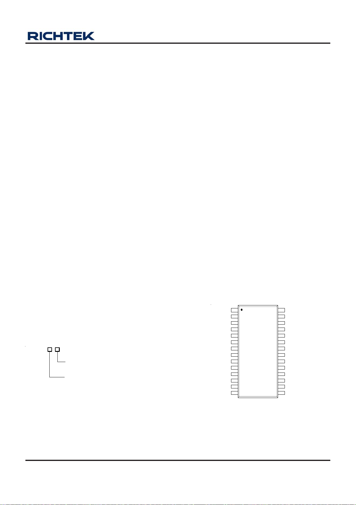
Pin Configurations
(TOP VIEW)
28
27
26
25
24
23
22
21
20
19
18
17
16
15
VCC
PWM1
PWM2
PWM3
ISN1
ISP1
ISP2
ISP3
ISN23
GND
ADJ
VDIF
VSEN
IMAX
VID4
VID3
VID2
VID1
VID0
VID125
SGND
FB
COMP
PGOOD
DVD
SS
RT
VOSS
2
3
4
5
6
7
8
9
10
11
12
13
14
TSSOP-28
DS9248-05 March 2007 www.richtek.com
1
Page 2
RT9248
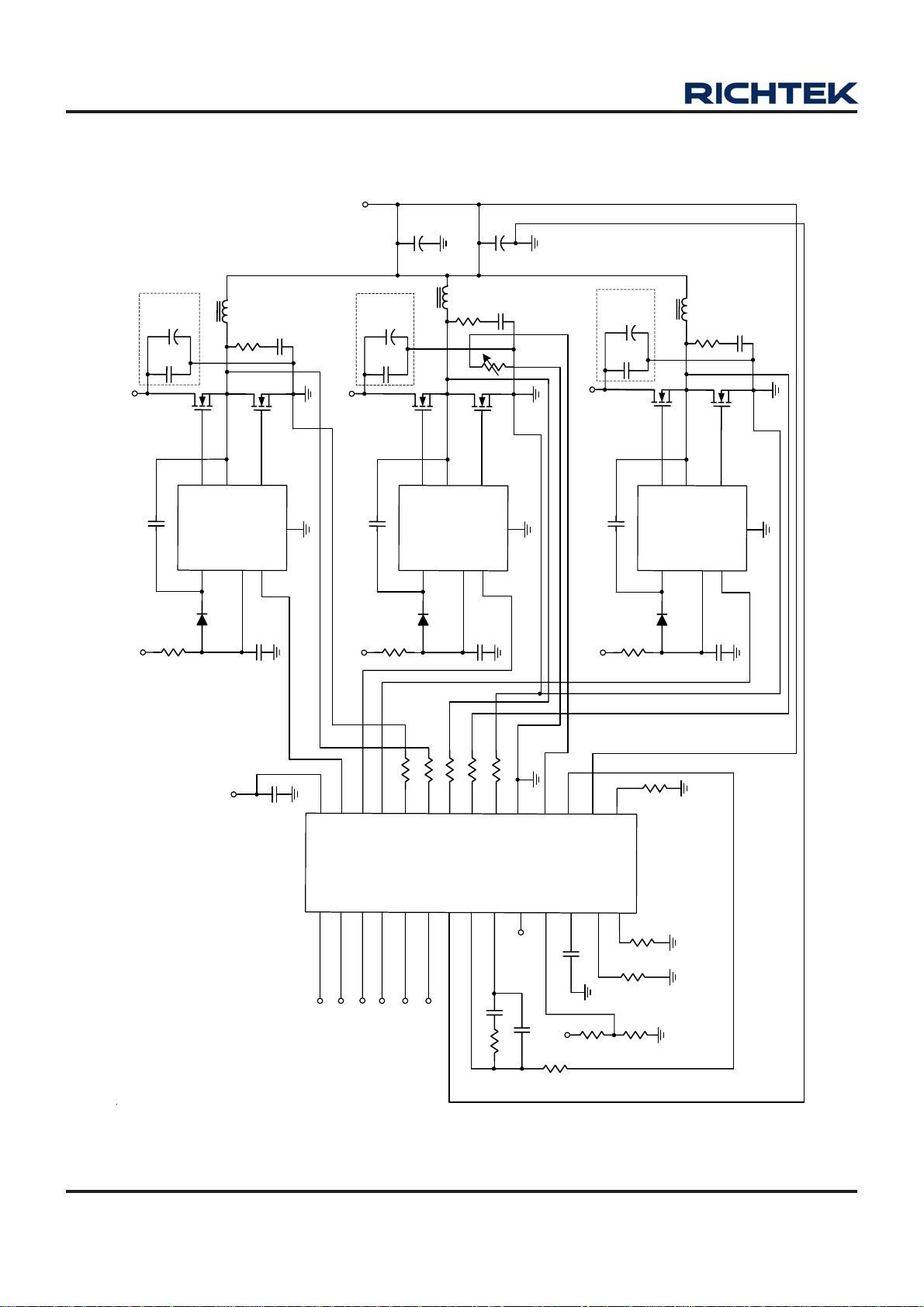
Typical Application Circuit
F
u
H
1
0
u
L
0
8
1
2
C
2
F
u
7
7
.
C
V
2
1
+
4
1
A
L
Q
3
0
N
9
0
D
P
I
7
8
H
W
V
S
R
3
D
0
F
6
u
C
V
2
1
+
6
1
9
T
R
T
S
B
4
1
8
4
1
1
4
D
N
1
3
1
0
R
1
F
u
1
4
0
9
7
.
1
.
C
0
4
R
2
A
L
Q
3
0
N
6
0
D
P
I
5
L
V
R
D
D
N
6
G
P
C
C
N
V
I
2
F
5
u
C
1
Preliminary
E
R
O
C
V
4
5
2
x
C
F
o
u
t
0
0
0
2
2
C
2
F
u
0
3
0
1
2
C
2
F
u
2
7
1
.
4
C
V
2
1
+
1
1
C
V
2
1
+
3
Q
8
3
0
F
u
6
1
9
T
R
1
8
4
1
2
4
D
N
1
5
1
0
R
1
8
4
2
x
C
F
o
u
t
0
5
0
2
2
2
C
F
H
2
u
L
1
A
L
3
0
N
9
0
D
P
I
7
H
W
V
S
R
D
T
S
B
4
u
1
4
6
0
1
7
.
1
.
C
0
4
R
V
2
1
4
A
Q
L
3
0
N
6
0
D
P
I
5
L
V
R
D
D
N
6
G
P
C
C
N
V
I
2
0
F
1
u
C
1
+
F
u
0
H
3
8
0
u
L
1
2
1
C
2
F
u
7
7
1
.
4
C
5
A
Q
L
3
0
N
9
0
D
P
I
7
8
H
W
V
S
R
3
0
6
F
1
u
1
C
V
2
1
+
D
6
9
T
R
T
S
B
4
1
8
4
3
1
D
4
N
7
1
1
0
R
1
F
u
1
9
0
8
1
.
7
1
.
0
C
4
R
6
A
Q
L
3
0
N
6
0
D
P
I
5
L
V
R
D
D
N
6
G
P
C
C
N
V
I
2
5
F
1
u
C
1
k
k
3
3
3
7
8
R
V
5
+
F
4
u
C
1
8
4
2
9
T
R
6
7
8
2
2
2
2
1
C
M
M
C
V
W
W
P
P
4
2
3
D
D
D
I
I
I
V
V
V
2
1
3
4
3
2
D
D
D
I
I
I
V
V
V
R
5
3
4
2
2
2
1
3
1
P
N
M
S
S
I
I
W
P
5
2
1
0
1
D
D
D
I
I
I
V
V
V
6
4
5
1
D
I
V
5
0
2
D
I
1
V
D
I
V
.
3
1
0
1
9
1
1
R
R
R
2
0
1
2
2
2
2
3
P
P
S
S
I
I
D
N
G
B
S
F
8
7
9
F
n
2
2
1
C
1
k
5
R
1
8
9
1
1
3
D
2
N
N
G
S
I
D
P
O
M
O
O
G
P
C
0
1
1
1
E
R
O
C
V
_
G
P
F
p
3
3
2
C
6
7
1
J
D
A
D
V
D
2
1
3
C
V
2
1
+
k
2
4
R
.
2
5
1
1
F
N
I
E
D
S
V
V
T
S
S
R
3
1
F
u
1
.
0
k
3
9
R
k
2
2
1
1
R
X
A
M
I
S
S
O
V
4
1
k
6
0
R
0
1
k
5
2
R
1
k
4
1
R
k
5
k
k
DS9248-05 March 2007www.richtek.com
2
Page 3
Preliminary
Functional Pin Description
VID4 (Pin 1), VID3 (Pin 2), VID2 (Pin 3), VID1 (Pin 4),
VID0 (Pin 5) & VID125 (Pin 6)
DAC voltage identification inputs. T ie VID125 to GND fo r
VRM9 or to VCC for VRD10. These pins are internally
pulled to 3.3V if left open.
RT9248
VOSS (Pin 14)
V
initial value offset. Connect this pin to GND with a
CORE
resistor to set the offset value.
IMAX (Pin 15)
Over-Current protection set.
SGND (Pin 7)
V
differential sense negative input.
CORE
FB (Pin 8)
Inverting input of the internal error a mplifier .
COMP (Pin 9)
Output of the error amplifier and input of the PWM
comparator.
PGOOD (Pin 10)
Power good open-drain output.
D V D (Pin 1 1)
Programma ble power UVLO detection or converter enable
input.
SS (Pin 12)
Connect this SS pin to GND with a capacitor to set the
soft-start time interval.
VSEN (Pin 16)
V
differential sense positive input.
CORE
V DIF (Pin 17)
V
differential sense output.
CORE
ADJ (Pin 18)
Current sense output for active droop adjust. Connect a
resistor from this pin to G ND to set the load droop.
GND (Pin 19)
IC ground.
ISN23 (Pin 20)
R
current sense inputs from converter 2nd & 3rd phase
DS(ON)
channel sense components' GND node.
ISP1 (Pin 23), ISP2 (Pin 22), ISP3 (Pin 21)
R
current sense inputs for individual converter
DS(ON)
channels. Tie this pin to the component's sense node.
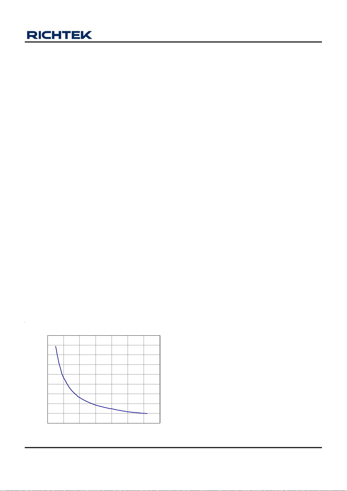
RT (Pin 13)
Switching frequency setting. Connect this pin to GN D with
a resistor to set the frequency.
450
400
350
300
250
(kHz)
200
OSC
f
150
100
50
0
0 10203040506070
DS9248-05 March 2007 www.richtek.com
Frequency vs. R
R
RT
RT
(k Ω)
ISN1 (Pin 24)
R
DS(ON)
current sense inputs from converter 1
st
channel
sense component's GND node.
PWM1 (Pin 27), PWM2 (Pin 26), PWM3 (Pin 25)
PWM outputs for ea ch driven channel. Connect these pins
to the PWM input of the MOSFET driver. For systems
which use 2 channels, connect PWM3 high.
VCC (Pin 28)
IC power supply . Connect this pin to a 5V supply.
3
Page 4
RT9248
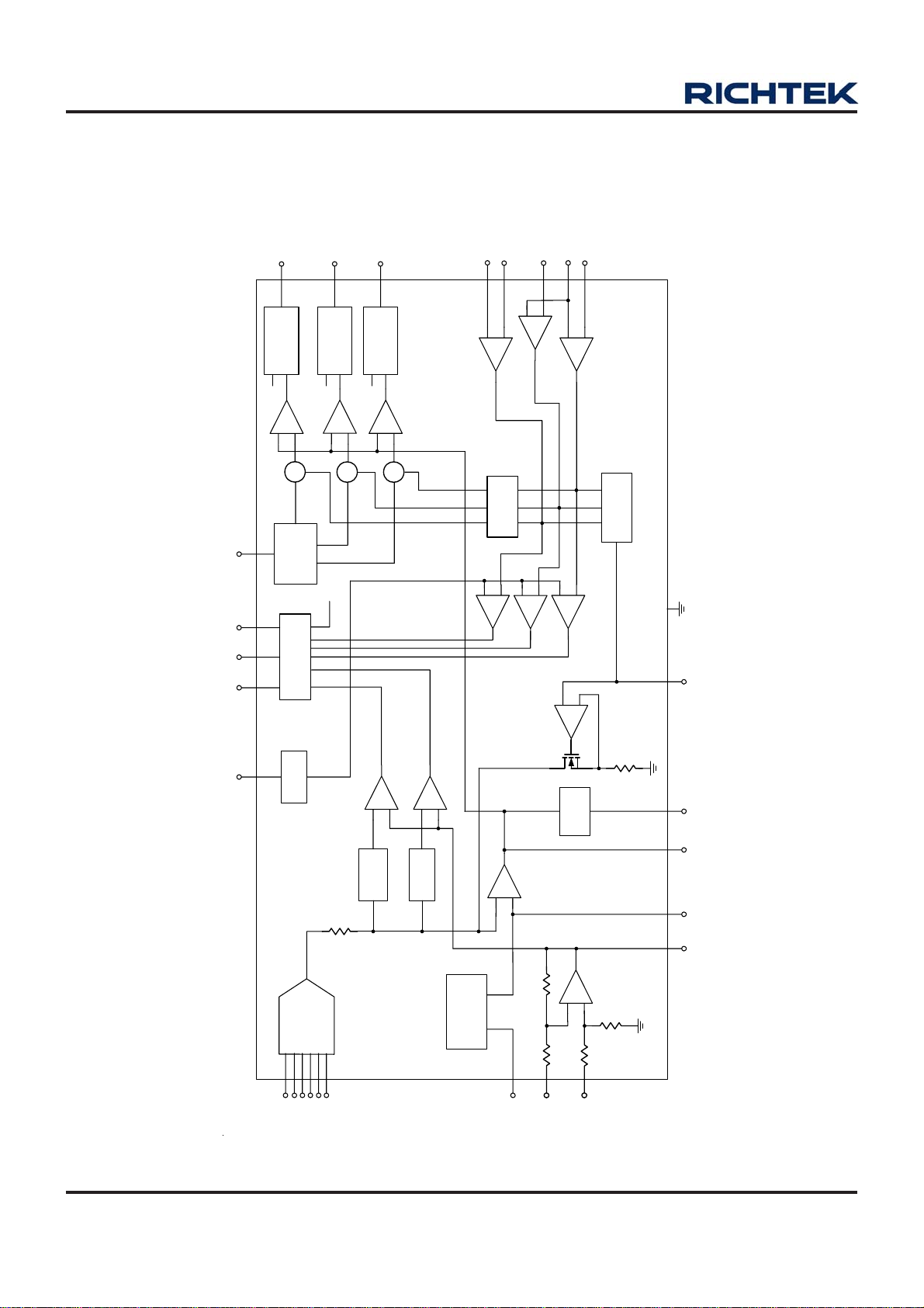
Function Block Diagram
Preliminary
PGOOD VCC DVD RT
PWM1
& Driver
PWM Logic
INH
-
+
+
+
Oscillator&Sawtooth
Power On Reset
INH
PWMCP
PWM2
& Driver
PWM Logic
-
+
PWMCP
+
+
INH
PWM3
& Driver
PWM Logic
INH
-
+
+
+
ISN1
ISP1
ISP2
ISN23
ISP3
+
-
+
-
PWMCP
Current
Correction
+
-
+
-
SUM/M
+
+
-
-
GND
ADJ
+
-
IMAX
GAP
Amplifier
OCP
Setting
DAC
VID1
VID3
VID4
VID0
VID2
VID125
-
+
Point
OVP Trip
-
+
Point
PG Trip
DAC + Droop
Source/Sink
Offset Currrent
SS
Control
-
+
Error
Amplifier
-
+
Buffer
Amplifier
VOSS
VSEN
SGND
SS
COMPVDIF FB
DS9248-05 March 2007www.richtek.com
4
Page 5
Preliminary
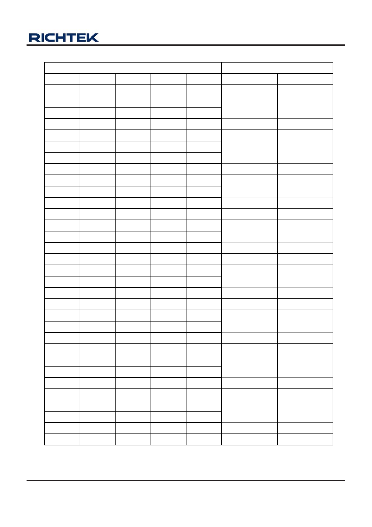
Table 1. Output Voltage Program
Pin Name Nominal Output Voltage DACOUT
VID4 VID3 VID2 VID1 VID0 VID125 = H VID125 = L
1 1 1 1 1 No CPU No CPU
0 1 0 0 1 0.850V 1.625V
0 1 0 0 0 0.875V 1.650V
0 0 1 1 1 0.900V 1.675V
0 0 1 1 0 0.925V 1.700V
0 0 1 0 1 0.950V 1.725V
0 0 1 0 0 0.975V 1.750V
0 0 0 1 1 1.000V 1.775V
0 0 0 1 0 1.025V 1.800V
0 0 0 0 1 1.050V 1.825V
0 0 0 0 0 1.075V 1.850V
1 1 1 1 0 1.100V 1.100V
RT9248
1 1 1 0 1 1.125V 1.125V
1 1 1 0 0 1.150V 1.150V
1 1 0 1 1 1.175V 1.175V
1 1 0 1 0 1.200V 1.200V
1 1 0 0 1 1.225V 1.225V
1 1 0 0 0 1.250V 1.250V
1 0 1 1 1 1.275V 1.275V
1 0 1 1 0 1.300V 1.300V
1 0 1 0 1 1.325V 1.325V
1 0 1 0 0 1.350V 1.350V
1 0 0 1 1 1.375V 1.375V
1 0 0 1 0 1.400V 1.400V
1 0 0 0 1 1.425V 1.425V
1 0 0 0 0 1.450V 1.450V
0 1 1 1 1 1.475V 1.475V
0 1 1 1 0 1.500V 1.500V
0 1 1 0 1 1.525V 1.525V
0 1 1 0 0 1.550V 1.550V
0 1 0 1 1 1.575V 1.575V
0 1 0 1 0 1.600V 1.600V
Note:(1) 0: Connected to GND
(2) 1: Open
(3) For VID125, H: VCC, L: GND
DS9248-05 March 2007 www.richtek.com
5
Page 6
RT9248
Preliminary
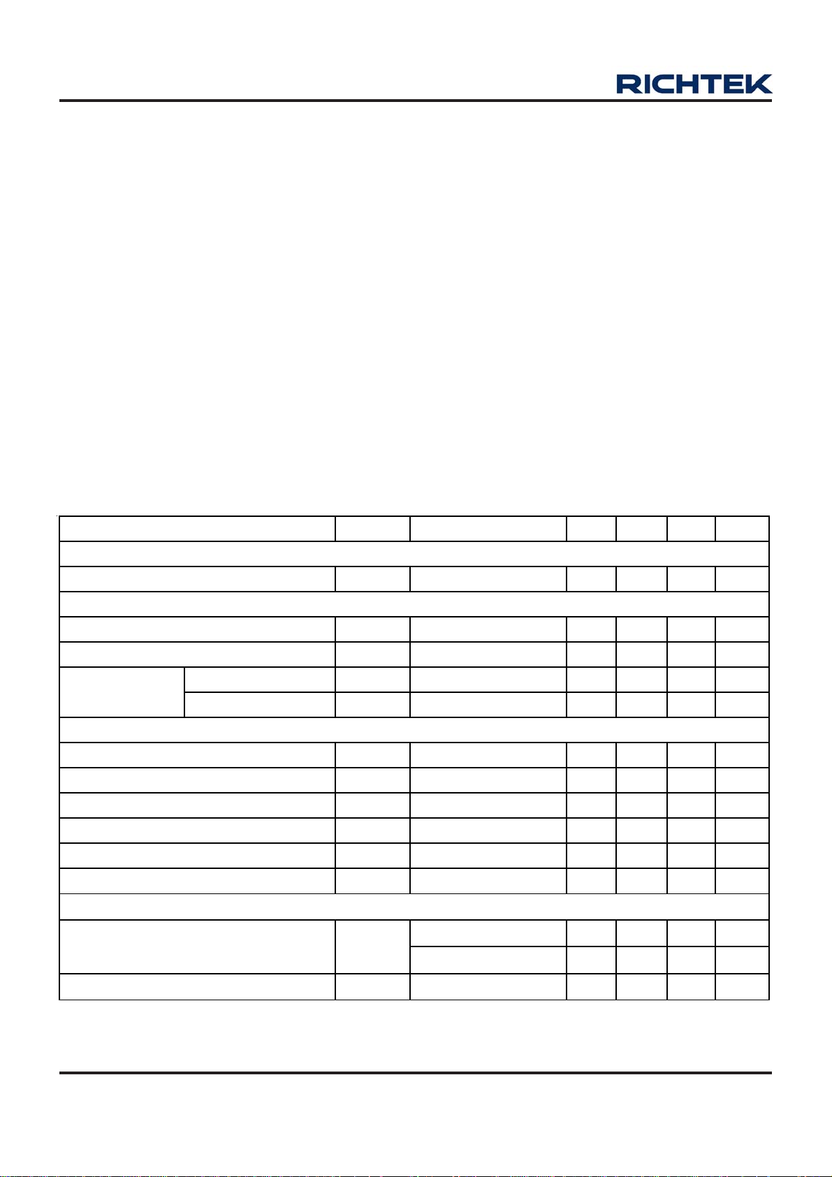
Absolute Maximum Ratings (Note 1)
z Supply Voltage, V
z Input, Output or I/O Voltage---------------------------------------------------------------------------------- GND-0.3V to V
z Package Thermal Resista nce
------------------------------------------------------------------------------------------- 7V
CC
TSSOP-28, θJA-------------------------------------------------------------------------------------------------- 45°C/W
z Junction T emperature------------------------------------------------------------------------------------------ 150°C
z Lead T e mperature (Soldering, 10 sec.)-------------------------------------------------------------------- 260°C
z Storage T emperature Range --------------------------------------------------------------------------------- −65°C to 150°C
z ESD Susceptibility (Note 2)
HBM (Human Body Mode) ----------------------------------------------------------------------------------- 2kV
MM (Ma chine Mode)------------------------------------------------------------------------------------------- 200V
Recommended Operating Conditions (Note 3)
z Supply Voltage, V
z Ambient T emperature Range--------------------------------------------------------------------------------- 0°C to 70°C
z Junction T emperature Range--------------------------------------------------------------------------------- 0°C to 125°C
Electrical Characteristics
(V
= 5V, T
CC
= 25° C, unless otherwise specified)
A
VCC Supply Current
------------------------------------------------------------------------------------------- 5V ± 10%
CC
Parameter Symbol Test Conditions Min Typ Max Units
CC
+0.3V
Nominal Supply Current ICC PWM 1,2,3 Open
--
12 -- mA
Power-On Reset
POR Threshold V
Hysteresis V
Trip (Low to High) V
V
Threshold
DVD
Hysteresis V
VCC Rising 4.0 4.2 4.5 V
CCRTH
0.2 0.5 -- V
CCHYS
Enable 0.95 1.0 1.05 V
DVDTP
-- 70 -- mV
DVDHYS
Oscillator
Free Running Frequency f
Frequency Adjustable Range f
Ramp Amplitude
OSC
50 -- 400 kHz
OSC_ADJ
RRT = 12kΩ
ΔV
OSC
R
RT
= 12kΩ
170 200 230 kHz
-- 1.9 -- V
Ramp Val ley VRV -- 1.0 -- V
Maximum On-Time of Each Channel 62 66 75 %
RT Pin Voltage VRT
R
RT
= 12kΩ
0.55 0.60 0.65 V
Reference and DAC
DACOUT Voltage Accuracy
ΔV
DAC_10
VRD10, V
VRD10, V
≥ 1V −1
DAC
< 1V
DAC
−10
-- +1 %
-- +10 mV
DACOUT Voltage Accuracy
6
ΔV
DAC_9
VRM9
−1
-- +1 %
To be continued
DS9248-05 March 2007www.richtek.com
Page 7
Preliminary
RT9248
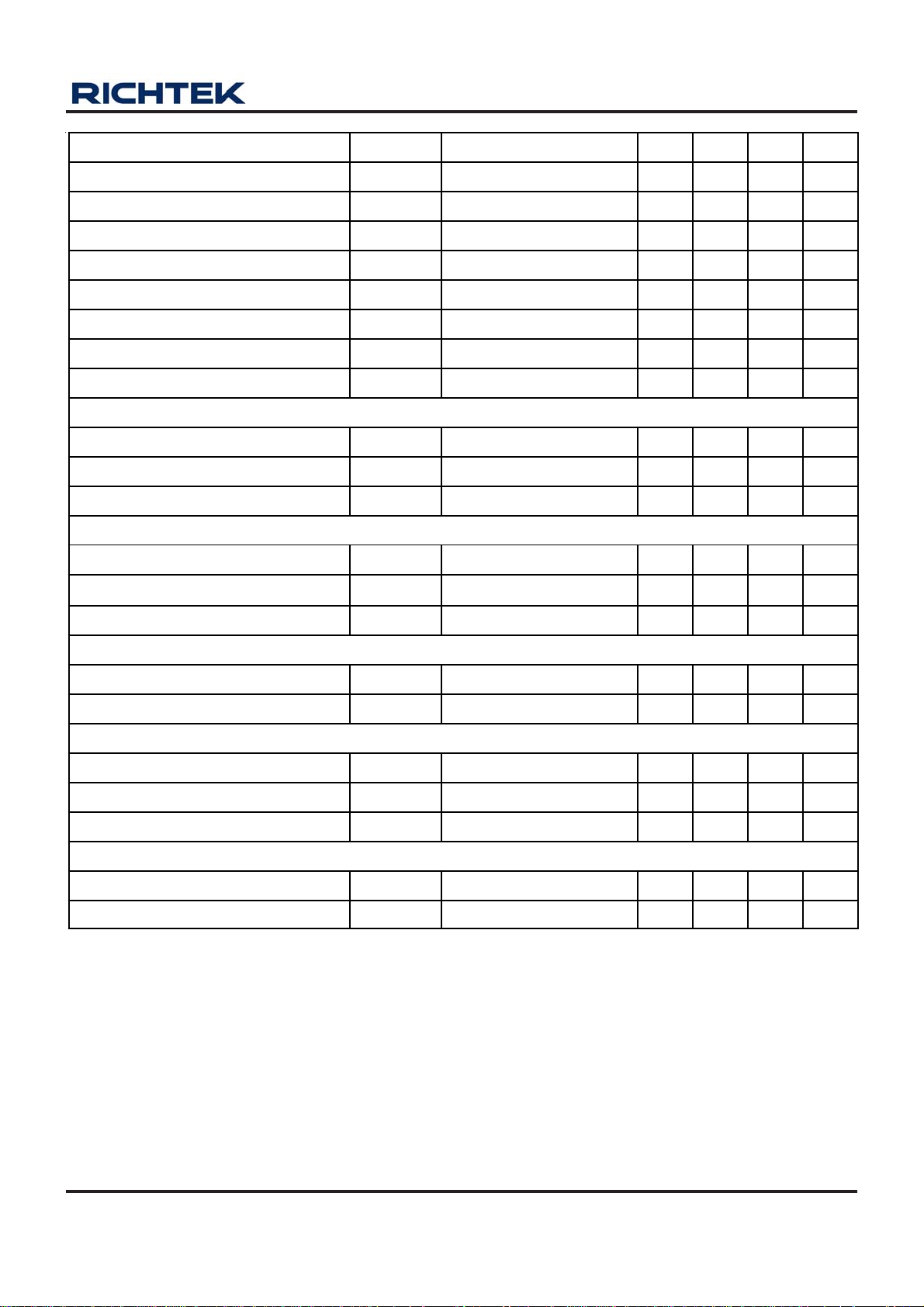
Parameter Symbol Test Conditions Min Typ Max Units
DAC (VID0-VID4) Input Low
DAC (VID0-VID4) Input High
DAC (VID0-VID4 ) Input Low
DAC (VID0-VID4) Input High
VID125 Input for VRM9
VID125 Input for VRD10
DAC (VID0-VID125) Bias Current
VOSS Pin Voltage
V
ILDAC_10
V
IHDAC_10
V
ILDAC_9
V
IHDAC_9
V
VID125_9
V
VID125_10
I
BIAS_DAC
V
VOSS
VRD10 -- -- 0.4 V
VRD10 0.8 -- -- V
VRM9 -- -- 0.8 V
VRM9 2.2 -- -- V
-- -- 0.4 V
0.8 -- -- V
60 120 180
R
VOSS
= 100kΩ
0.95 1.0 1.05 V
μA
Error Amplifier
DC Gain -- 85 -- dB
Gain-Bandwidth Product GBW -- 10 -- MHz
Slew Rate SR COMP = 10pF -- 3 --
V/μs
Differential Sense Amplifier
Input Impedance
Z
IMP
-- 16 --
kΩ
Gain-Bandwidth Product GBW -- 10 -- MHz
Slew Rate SR -- 3 --
V/μs
Current Sense GM Amplifier
ISP 1,2,3 Full Scale Source Current
ISP 1,2,3 Current for OCP
I
ISPFSS
I
ISPOCP
60 -- - 90 -- --
μA
μA
Protection
IMAX Voltage
SS Current
Over-Voltage Trip (VSEN/DACOUT)
V
IMAX
I
SS
ΔOVT
= 10k 0.55 0.60 0.65 V
R
IMAX
= 1V -- 13 --
V
SS
-- 140 -- %
μA
Power Good
Lower Threshold (VSEN/DACOUT)
Output Low Voltage
Note 1. Stresses listed as the above “Absolute Maximum Ratings” may cause permanent damage to the device. These are
for stress ratings. Functional operation of the device at these or any other conditions beyond those indicated in the
operational sections of the specifications is not implied. Exposure to absolute maximum rating conditions for extended
periods may remain possibility to affect device reliability.
Note 2. Devices are ESD sensitive. Handling precaution recommended
Note 3. The device is not guaranteed to function outside its operating conditions.
V
V
PG−
PGL
VSEN Rising -- 92 -- %
= 4mA -- -- 0.2 V
I
PG
DS9248-05 March 2007 www.richtek.com
7
Page 8
RT9248
Application Information
Preliminary
RT9248 is a multi-phase DC/DC controller that precisely
regulates CPU core voltage and balances the current of
different power channels. The converter consisting of
RT9248 and its compa nion MOSFET driver provides high
quality CPU power and all protection functions to meet
the requirement of modern VRM.
Voltage Control
RT9248 senses the CPU V
by an precise instrumental
CORE
amplifier to minimize the voltage drop on PCB trace at
heavy load. VSEN & SGND are the dif ferential inputs. V DIF
is the output node of the differential voltage & the input for
PGOOD & OVP sense. The internal high accuracy VID
DAC allows selection of either VRM9 or V RD10 complia nce
via VID125 pin setting. Control loop consists of error
amplifier, multi-phase pulse width modulator, driver and
power components. Like conventional voltage mode PWM
controller, the output voltage is locked at the V
REF
of error
amplif ier and the error sign al is used a s the control signal
VC of pulse width modulator. The PWM sign als of different
channels are generated by comparison of EA output a nd
split-phase sawtooth wave. Power stage tra nsf orms V
to
IN
output by PWM signal on-time ratio.
Current Balance
RT9248 senses the current of low side MOSFET in each
synchronous rectifier when it is conducting for channel
current balance and droop tuning. The differential sensing
GM amplif ier converts the voltage on the sense component
(can be a sense resistor or the R
of the low side
DS(ON)
MOSFET) to current signal into internal balance circuit.
The current balance circuit sums a nd averages the current
signals then produces the balancing signals injected to
pulse width modulator. If the current of some power cha nnel
is greater than average, the bala ncing signal reduces the
output pulse width to keep the balance.
Load Droop
The sensed power channel current signals regulate the
reference of DAC to f orm a output voltage droop proportional
to the load current. The droop or so-called “active voltage
positioning” can reduce the output voltage ripple at load
transient a nd the LC filter size.
Fault Detection
The chip detects V
for over voltage a nd power good
CORE
detection. The “hiccup mode” operation of over-current
protection is adopted to reduce the short circuit current.
The inrush current at the start up is suppressed by the
soft start circuit through clamping the pulse width a nd output
voltage.
Phase Setting and Converter Start Up
RT9248 interfac es with companion MOSFET drivers (like
RT9600, RT9602 or RT9603 series) for correct converter
initialization. The tri-state PWM output (high, low a nd high
impedance) pins sense the interface voltage at IC POR
period (both VCC and D V D trip). The channel is enabled if
the pin voltage is 1.2V less than VCC. Please tie the PWM
output to VCC and the current sense pins to GND or left
floating if the channel is unused. For 2-Cha nnel application,
connect PWM3 high.
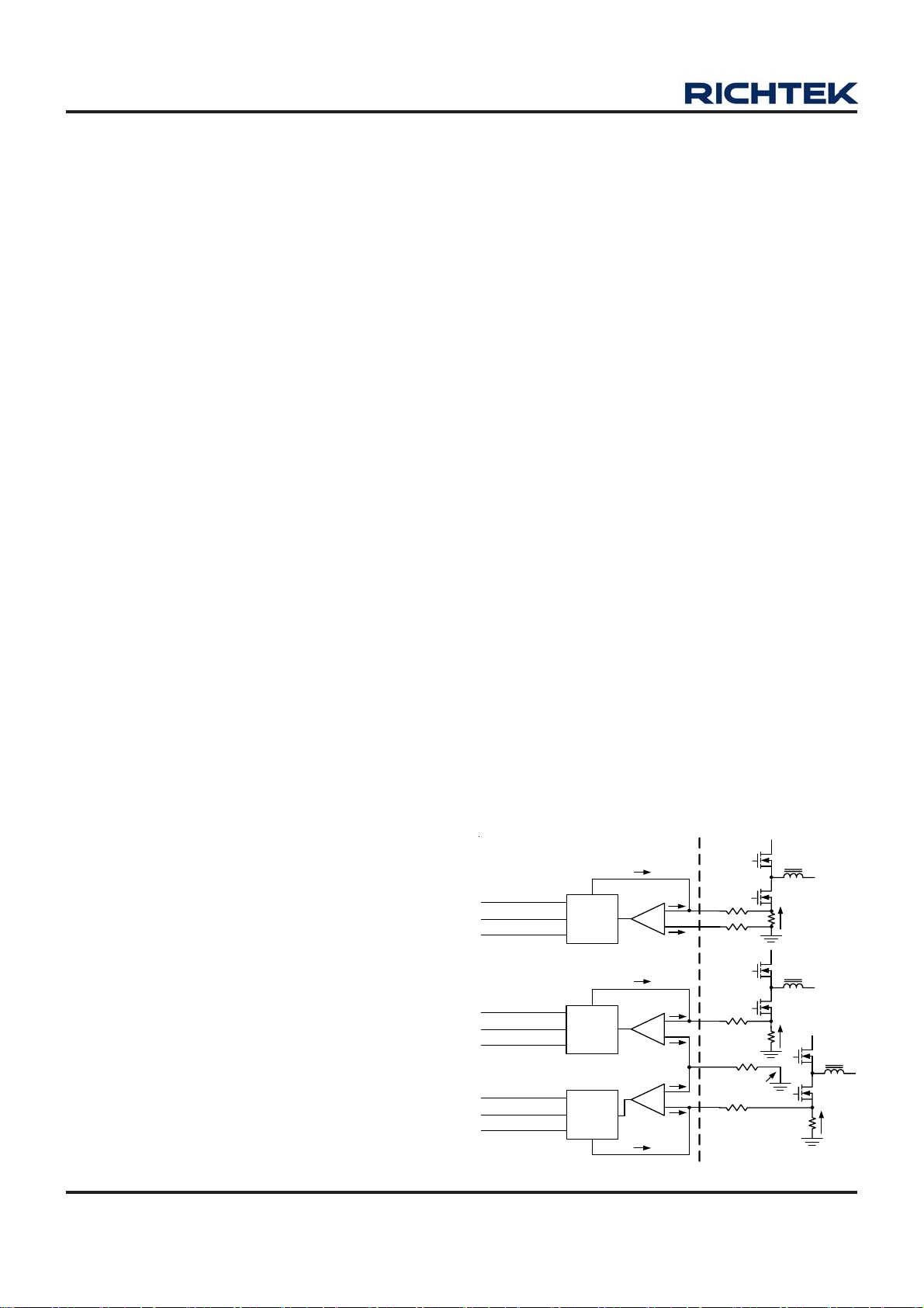
Current Sensing Setting
RT9248 senses the current of low side MOSFET in each
synchronous rectifier when it is conducting for channel
current balance a nd droop tuning. The differential sensing
GM amplif ier converts the voltage on the sense component
(can be a sense resistor or the R
of the low side
DS(ON)
MOSFET) to current signal into internal circuit (see
Figure 1). Be careful to choose GND sense input ISN23 of
GM amplifier of channel 2 & 3 (tied together by internal
wiring) for effective cha nnel current balance.
I
X1
Current
Balance
<
Droop Tune
<
<
Over-Current
Detection
Current
Balance
<
Droop Tune
<
<
Over-Current
Detection
Current
Balance
<
Droop Tune
<
<
Over-Current
Detection
I
X
Sample
2I
X
&
I
Hold
X
I
X
Sample
2I
X
&
I
Hold
X
I
X
Sample
2I
X
&
I
Hold
X
I
BP
-
GM
+
I
BN
I
X2
I
BP
-
GM
+
I
BN
I
BN
+
GM
-
I
BP
I
X3
ISP1
ISN1
ISP2
ISN23
Channel 2 & 3
GND return
ISP3
R
SP1
R
I
S
SN23
L
R
I
S
L
R
I
S
L
R
SN1
R
SP2
R
R
SP3
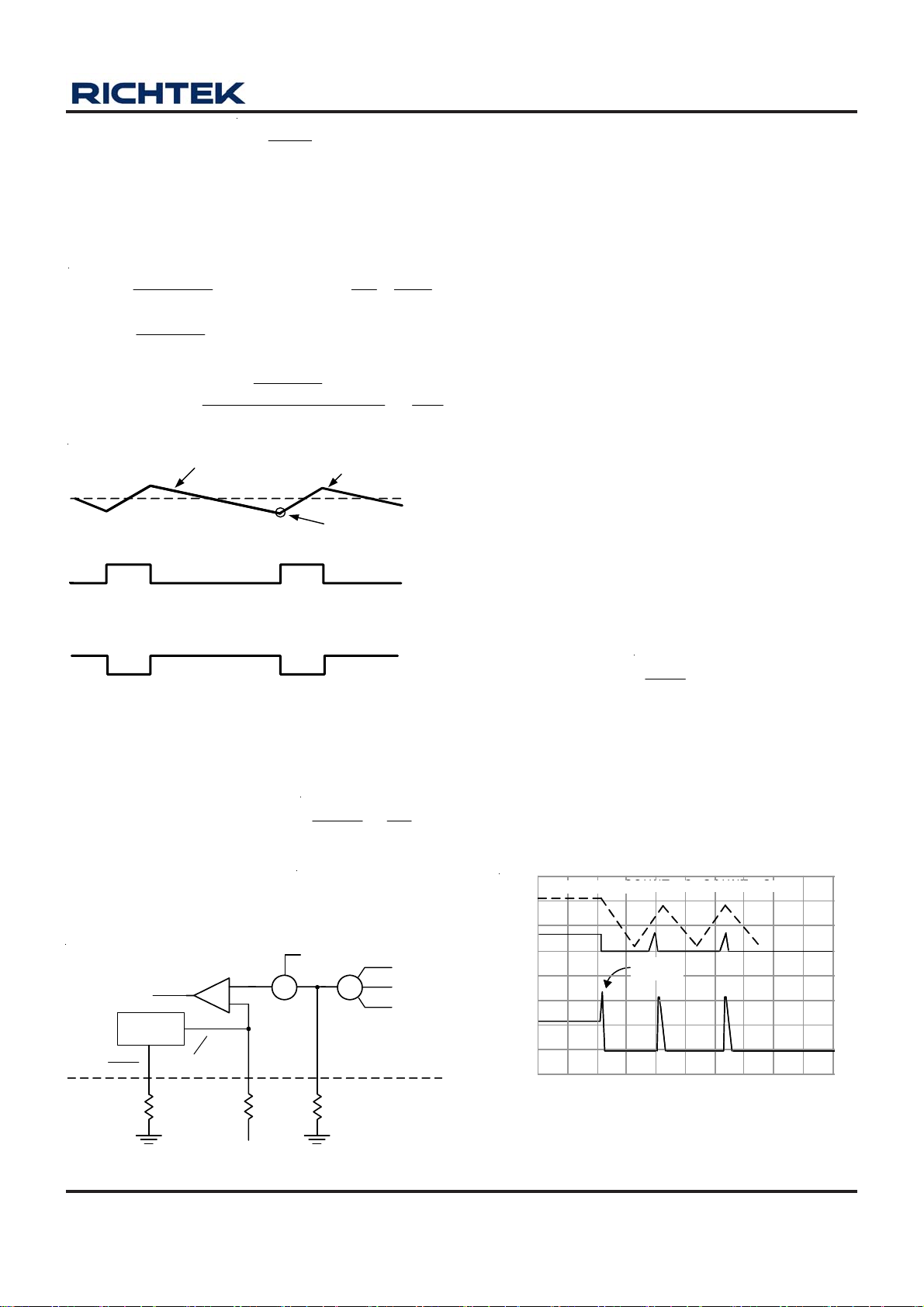
Figure 1. Current Sense Circuit
DS9248-05 March 2007www.richtek.com
8
Page 9
Preliminary
RI
×
I
=
The sensing circuit gets by local feedback.
R
= RSN for channel 1 & R
SP
X
SP
3 phase operation) to cancel the voltage drop caused by
GM amplif ier input bia s current. I
before low side MOSFET turns off (See Figure 2).
Therefore,
S(S/H) L
×
(S/H) X
=
I
⎡
OFF
=
T
⎢
⎣
⎡
⎢
⎢
II
RI
SP
R
OIN
−
VV
⎤
⎥
IN
V
⎦
⎡
O
−
V
⎢
L(AVG)(S/H) X
−=
⎣
⎢
⎢
⎣
Falling Slope = Vo/L
Inductor Current
PWM Signal & High Side MOSFET Gate Signal
Low Side MOSFET Gate Signal
Figure 2. Inductor Current and PWM Signal
DAC Offset V oltage & Droop Tuning
The DAC off set voltage is set by compensation network
& VOSS pin external resistors by .
The S/H current signals from power channels are inje cted
to ADJ pin to create droop voltage.
The DAC output voltage decreases by V
V
load droop (see Figure 3).
CORE
I =
VOSS
R
V1
VOSS
Current
Source
>
COMP
V
OSS
R
VOSS
+
EA
-
>
1
VOSSI
4
+
FB ADJ
R
-
>
V
CORE
Figure 3. DAC Offset V oltage & Droop Tune Circuit
SL
SP
R
= 2R
for channel 2 & 3 (at
SN
is sampled a nd held just
X
(AVG) L(S/H) L
I I ,
V
×−=
L
=×
200kHzfosc for 5uS
OIN
−
VV
⎤
5uS
×
⎥
IN
V
⎦
2L
I
L
I
L(S/H)
V1
VOSS
ADJ
∑
R
ADJ
⎞
×
⎟
⎠
×= XADJADJ I 2RV
∑
to form the
⎛
⎜
R
⎝
V
DAC
+
V
ADJ
-
F1
⎤
⎥
⎥
⎥
⎥
⎦
R
T
×
1f
4
2I
2I
2I
OFFO
2
S
R
SP
R
I
L(AVG)
X1
X2
X3
RT9248
Protection and SS Function
For OVP , the RT9248 detects the V
of the differential a mplifier output. Eliminate the delay due
to compensation network (compared to sensing FB voltage)
for fast and accurate detection. The trip point of OVP is
140% of normal output level. The PWM outputs are pulled
low to turn on the low side MOSFET and turn of f the high
,
side MOSFET of the synchronous rectifier at OVP. The
OVP latch can only be reset by VCC or D V D restart power
on reset sequence. The PGOOD detection trip point of
V
is 92% lower than the normal level. The PGOOD
CORE
open drain output pulls low when V
trip point. For VID jumping issue, only power fail conditions
(VCC & DVD are lower than trip point or OVP) reset the
output low.
Soft-start circuit generates a ramp voltage by charging
external capacitor with 13μA current after IC POR acts.
The PWM pulse width and V
CORE
ramp to reduce the inrush current and protect the power
devices.
Over-current protection trip point is set by the resistor R
connected to IMAX pin. OCP is triggered if one channel
V6.0
S/H current signal IX > Controller forces
⎛
⎜
⎝
⎞
⎟
IMAX
R
⎠
PWM output latched at high impedance to turn off both
high and low side MOSFETs in the power stage a nd initial
the hiccup mode protection. The SS pin voltage is pulled
low with a 13μA current after it is le ss than 90% VCC. The
converter restarts after SS pin voltage < 0.2V . Three times
of OCP disable the converter and only rele ase the latch by
POR acts (see Figure 4).
COUNT = 2 COUNT = 3
Count = 2 Count = 3
Overload
Applied
TIME
TIME
V
I
CORE
LOAD
S.S
0V
0A
COUNT = 1
Count = 1
T0,T1 T2
Figure 4.
by V
CORE
is lower than the
CORE
are clamped by the rising
.4.1
×
T3,T4
pin voltage
DIF
IMAX
DS9248-05 March 2007 www.richtek.com
9
Page 10
RT9248
Preliminary
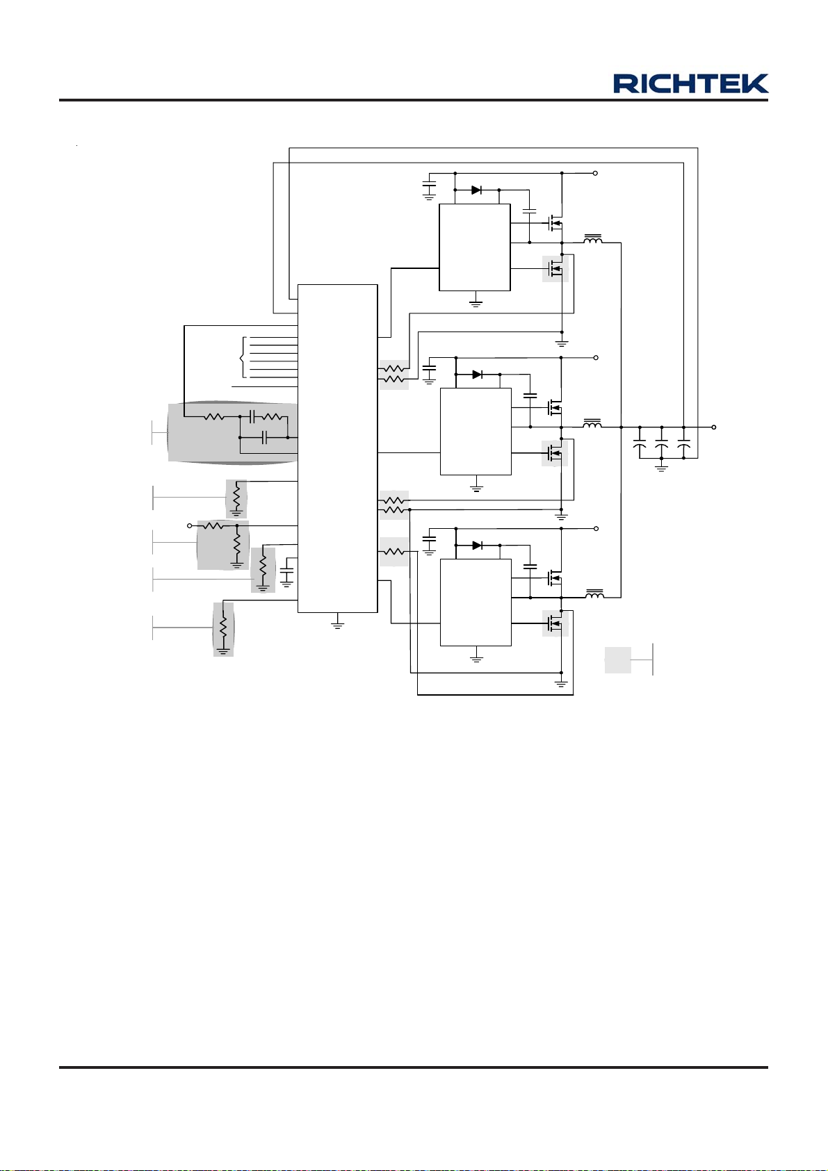
3-Phase Converter and Components Function Grouping
12V
Compensation
& Offset
Droop Setting
Driver Power
UVLO
DAC Offset
Voltage Setting
OCP Setting
12V
PGOOD
VID
SGND
VSEN
VDIF
RT9248
COMP
FB
ADJ
DVD
VOSS
SS
IMAX
GND
PWM1
ISP1
ISN1
PWM2
ISP2
ISN23
ISP3
PWM3
VCC
DRVH
RT9603
IN
DRVL
PGND
VCC
DRVH
RT9603
IN
DRVL
PGND
VCCINBST
DRVH
RT9603
DRVL
PGND
BST
SW
BST
SW
SW
12V
12V
Current Sense
Components
V
CORE
Design Procedure Suggestion
Voltage Loop Setting
a. Output filter pole and zero (Inductor , output ca pa citor
value & ESR).
b. Error amplif ier compensation & sawtooth wave a mp litude (compensation network).
c. Kelvin sense for V
Current Loop Setting
a. GM a mplif ier S/H current (current sense component
R
, ISPx & ISNx pin external resistor value,
DS(ON)
keep ISPx current < 60μA at full load condition for
better load line linearity).
b. Over-current protection trip point (IMAX pin resistor ,
keep ISPx current < 90μA at OCP condition for
precision issue).
10
CORE
.
VRM Load Line Setting
a. Droop a mplitude (ADJ pin resistor).
b. No loa d offset (a dditional resistor in compensation
network).
c. DAC off set voltage setting (VOSS pin & compen sation network resistor).
Power Sequence & SS
DVD pin external resistor and SS pin ca pa citor.
PCB Layout
a. Kelvin sense for current sense GM a mplif ier input.
b. Refer to layout guide for other item.
DS9248-05 March 2007www.richtek.com
Page 11
Preliminary
π
RT9248
Design Example
Given:
Apply f or three pha se converter
V
V
I
V
OCP trip point set at 30A for each channel (S/H)
R
L = 2μH
C
1. Compensation Setting
Modulator Gain = = = 4.2 (12.46dB)
where V
b. EA Compensation Network:
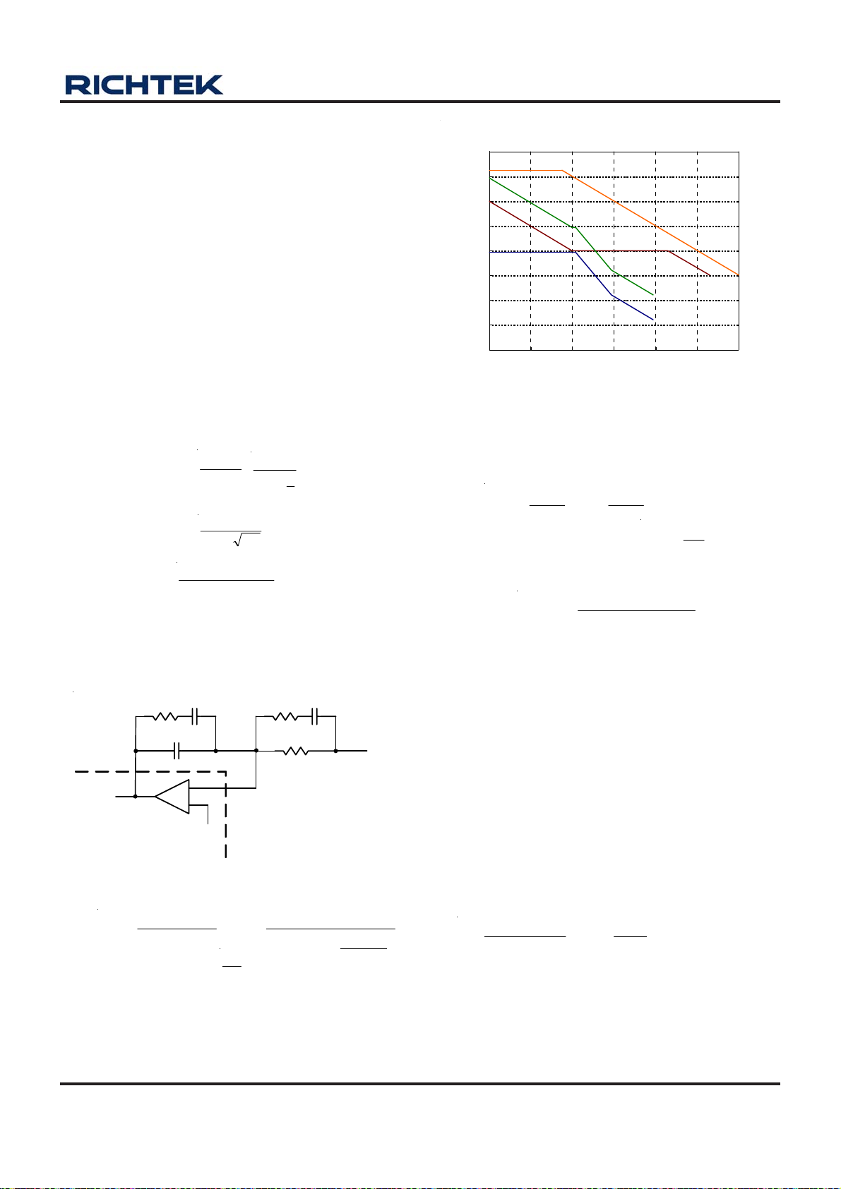
Select R1 = 2.4kΩ, R2 = 24kΩ, C1 = 6.6nF,
C2 = 33pF and use the type 2 compensation
scheme shown in Figure 5.
= 12V
IN
= 1.5V
CORE
(max) = 60A
LOAD
= 120mV at full load
DROOP
= 6mΩ of low side MOSFET at 27°C
DS(ON)
= 9,000μF with 2mΩ ESR.
OUT
a. Modulator Gain, Pole a nd Zero:
From the following formula:
IN
V
RAMP
V
: ramp amplitude of sawtooth wave
RAMP
LC Filter Pole = = 1.2kHz and
ESR Zero = = 8.8kHz
R
2
COMP
π
x ESR x C
2
C1
C2
+
DACOUT
12V
3
1.9V2×
1
LC x 2
1
OUT
C3
R
3
R
1
FB
R3,C3 are used in type
3 compensation scheme
(left NC in type 2)
>
VDIF
Asym ptotic Bode Plot of PWM Loop Gain
100
80
60
40
20
Gain (dB)
0
-20
-40
-60
10 100 1K 10K 100K 1M 10M
10 100 1000 10000 100000 1000000 10000000
Frequency (Hz)
Uncompensated EA Gain
Compensated EA Gain
PWM Loop Gain
Modulat o r Gain
Figure 6.
2. Droop & DAC Offset Setting
For each channel the load current is 60A / 3 = 20A
and the ripple current, ΔIL, is given as:
1.5V
x 5us =
2uH
The load current, IL, at S/H is
1.5V
⎛
1x
−
⎜
⎝
⎞
3.28A
⎟
12V
⎠
Δ
A20
−
I
L
=
2
.
A36.18
Using the following formula to select the appropriate
I
for the S/H of GM amplifier:
X (MAX)
(MAX) X
I
=
DS(ON)
18.36AR
×
SP
R
The suggested IX is in the order of 40 to 50μA, select
R
= R
SP
V
DROOP
R
, therefore R
ADJ
The R
= 2.4kΩ, then I
SN
= 120mV = 45.9μA × 2 × 3 (phase no.) ×
will be 435Ω.
ADJ
of MOSFET varies with temperature
DS(ON)
will be 45.9μA.
X (MAX)
rise. When the low side MOSFET working at 70°C
and 5000ppm/°C temperature coeff icient of R
the R
at 70°C is given as:
DS(ON)
DS(ON)
,
6mΩ × {1+ (70°C − 27°C) × 5000ppm/°C} = 7.3mΩ.
R
at 70°C is given as:
ADJ
R
ADJ_27°C
× (R
DS(ON)_27°C
/ R
DS(ON)_70°C
) = 358Ω
Figure 5.
From the following formulas:
Z
F
1
x R x 2
Cπ
Middle Band Gain =
By calculation, the FZ = 1kHz, F
==
P
1 2
F ,
R
R
π
2
1
P
Middle Band Gain is 10 (i.e 20dB).
1
×
CC
⎛
2
x R x 2
⎜
+
CC
⎝
= 200kHz and
21
⎞
⎟
21
⎠
3. Over-Current Protection Setting
OCP trip point set at 30A for ea ch cha nnel,
DS(ON)
X
I ×=
=
, R
30AR
×
R
1.4
0.6V
IMAXSP
R
IMAX
T a ke the temperature rise into a ccount, the R
70°C will be:
R
IMAX_27°C
× (R
DS(ON)_27°C
/ R
DS(ON)_70°C
= 11.2kΩ
IMAX
) = 9.2kΩ
at
The asymptotic bode plot of EA compensation and
PWM loop gain is shown as Figure 6.
DS9248-05 March 2007 www.richtek.com
4. Soft-Start Capacitor Selection
C
= 0.1μF is the suitable value for most application.
SS
11
Page 12
RT9248
Preliminary
Layout Guide
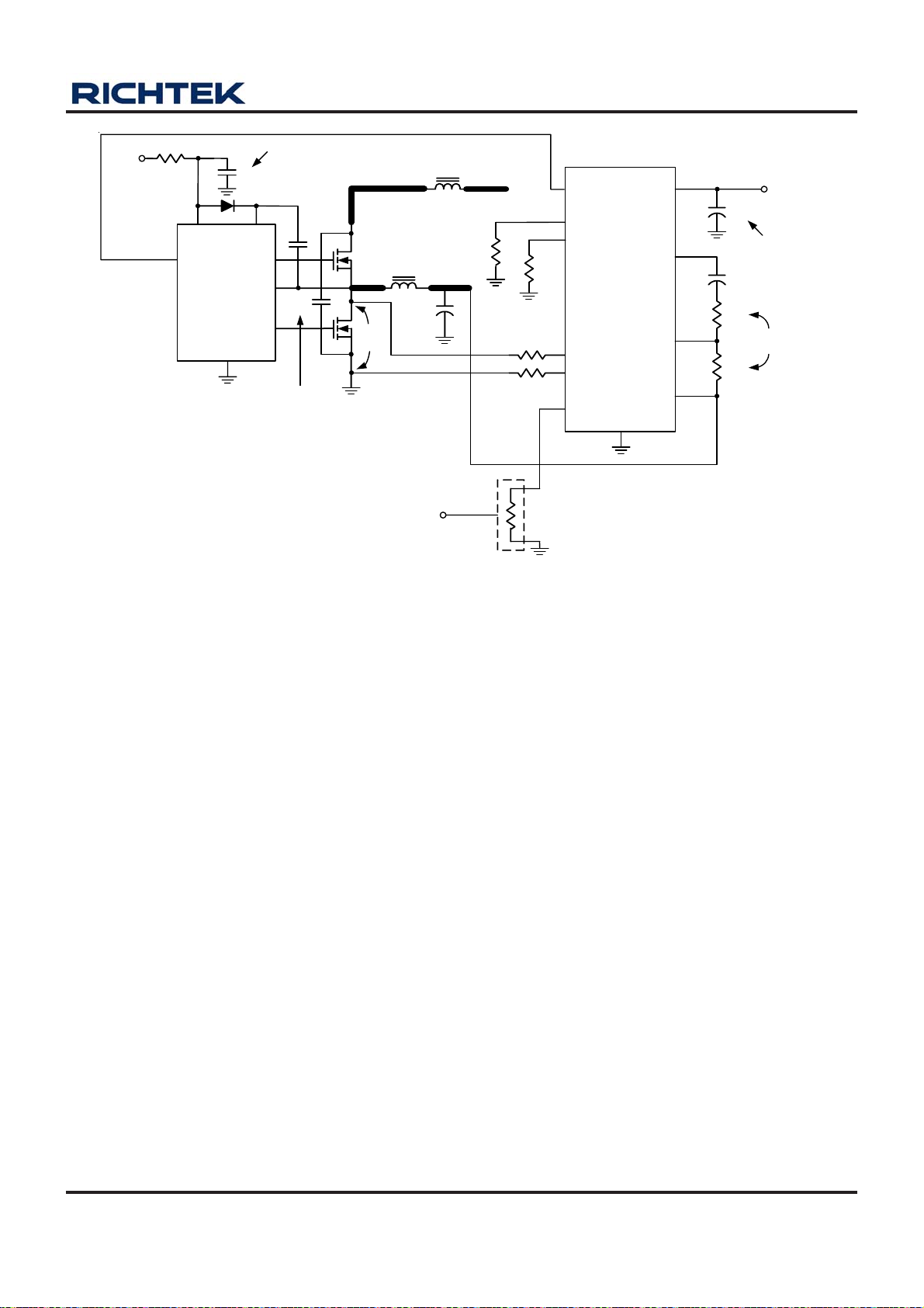
Place the high-power switching components first, a nd separate them from sensitive nodes.
1. Most critical path: the current sense circuit is the most sensitive part of the converter. The current sense
resistors tied to ISP1,2,3 and ISN1,ISN23 should be located not more than 0.5 inch from the IC and away
from the noise switching nodes. The PCB trace of sen se node s should be parallel and as short a s possible.
Kelvin connection of the sense component (additional sense resistor or MOSFET R
) ensures the accurate
DS(ON)
stable current sensing.
Keep well Kelvin sense to en sure the stable operation!
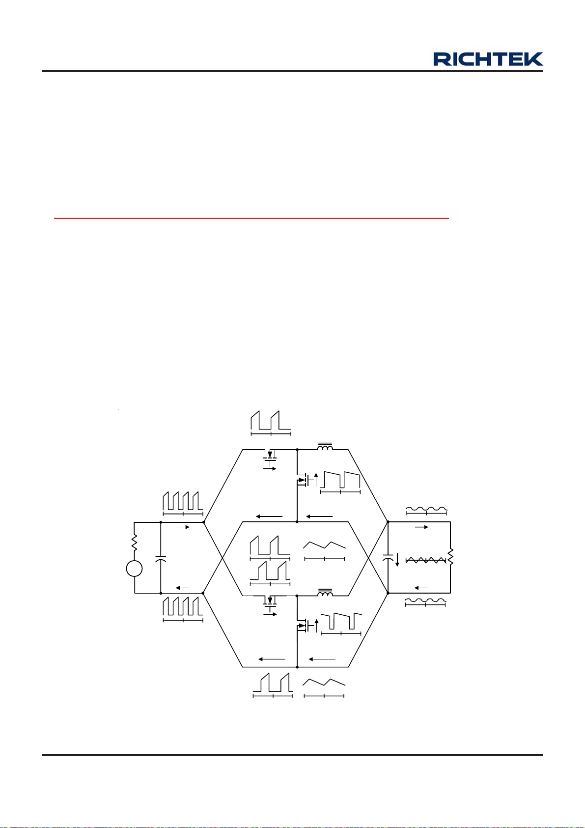
2. Switching ripple current path:
a. Input ca pa citor to high side MOSFET.
b. Low side MOSFET to output ca pa citor.
c. The return path of input and output ca p a citor .
d. Separate the power and signal GND.
e. The switching nodes (the connection node of high/low side MOSFET a nd inductor) is the most noisy points.
Keep them away from sensitive small-signal node.
f. Reduce parasitic R, L by minimum length, enough copper thickness a nd avoiding of vi a.
3. MOSFET driver should be closed to MOSFET .
4. The compensation, bypass and other function setting components should be ne ar the IC and away from the noisy
power path.
SW1
V
IN
R
IN
C
V
IN
SW2
L1
L2
V
OUT
C
OUT
R
L
12
Figure 7. Power Stage Ripple Current Path
DS9248-05 March 2007www.richtek.com
Page 13
Preliminary
RT9248
+12V
C
BP
VCC
IN
BST
DRVH
SW
RT9603
DRVL
PGND
Locate near MOSFETs
Next to IC
C
BOOT
C
IN
+12V or +5V
L
O1
V
CORE
C
OUT
Kelvin
Sense
For Thermal Couple
Figure 8. Layout Consideration
PWM
IMAX
VOSS
RT9248
R
SIP
ISPx
R
ISNx
SIN
ADJ
VCC
COMP
R
FB
R
VSEN
GND
C
BP
C
C
C
FB
+5V
IN
Next to IC
Locate next
to FB Pin
DS9248-05 March 2007 www.richtek.com
13
Page 14
RT9248
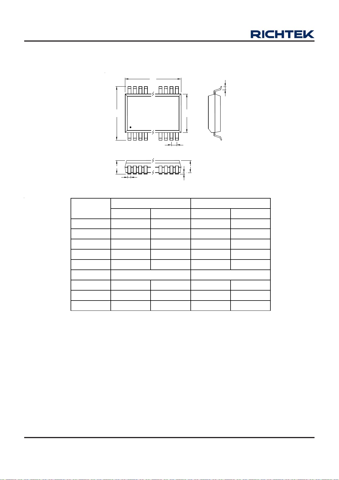
Outline Dimension
Preliminary
D
L
E
A
b
E1
e
A2
A1
Dimensions In M illimeters Dimen sions In Inches
Symbol
Min Max Min Max
A 0.850 1.200 0.033 0.047
A1 0.050 0.152 0.002 0.006
A2 0.800 1.050 0.031 0.041
b 0.178 0.305 0.007 0.012
D 9.601 9.804 0.378 0.386
e 0.650 0.026
E 6.300 6.500 0.248 0.256
E1 4.293 4.496 0.169 0.177
L 0.450 0.762 0.018 0.030
Richtek Technology Corporation
Headquarter
5F, No. 20, Taiyuen Street, Chupei City
Hsinchu, Taiwan, R.O.C.
Tel: (8863)5526789 Fax: (8863)5526611
14
28-Lead TSSOP Plastic Package
Richtek Technology Corporation
Taipei Office (Marketing)
8F, No. 137, Lane 235, Paochiao Road, Hsintien City
Taipei County, Taiwan, R.O.C.
Tel: (8862)89191466 Fax: (8862)89191465
Email: [email protected]
DS9248-05 March 2007www.richtek.com
 Loading...