

Page 1
Preliminary RT9600
Synchronous-Rectified Buck MOSFET Drivers
General Description
The RT9600 is a high frequency, dual MOSFET
driver specifically designed to drive two power NChannel MOSFETs in a synchronous-rectified buck
converter topology. This driver combined with the
RT9237/RT9241 series of Multi-Phase Buck PWM
controller form a complete core-voltage regulator
solution for advanced microprocessors.
The RT9600 drives both the lower/upper gate in a
synchronous-rectifier bridge with 12V. Independent
driving of upper gate through PVCC pin is
achievable. This drive-voltage flexibility provides the
advantage of optimizing applications involving tradeoffs between switching losses and conduction losses.
The output drivers in the RT9600 can efficiently
switch power MOSFETs at frequency up to 500KHz.
Switching frequency above 500KHz has to take into
account the thermal dissipation of SOP-8 package.
RT9600 is capable of driving a 3000pF load with a
30ns rise time. RT9600 implements bootstrapping on
the upper gate with only an external capacitor
required. This reduces implementation complexity
and allows the use of higher performance, cost
effective, N-Channel MOSFETs. Adaptive shootthrough protection is integrated to prevent both
MOSFETs from conducting simultaneously.
Features
z Drives Two N-Channel MOSFETs
z Adaptive Shoot-Through Protection
z Internal Bootstrap Device
z Supports High Switching Frequency
− Fast Output Rise Time
z Small SOP-8 Package
z Dual Gate-Drive Voltages for Optimal Efficiency
z Tri-State Input for Bridge Shutdown
z Supply Under Voltage Protection
Applications
z Core Voltage Supplies for Intel Pentium
AthlonTM Microprocessors
z High Frequency Low Profile DC-DC Converters
z High Current Low Voltage DC-DC Converters
4, AMD
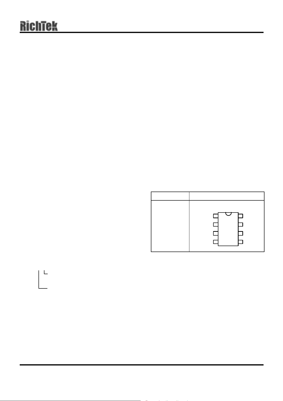
Pin Configurations
Part Number Pin Configurations
RT9600CS
(Plastic SOP-8)
UGATE
BOOT
PWM
GND
TOP VIEW
1
2
3
4
8
7
6
5
PHASE
PVCC
VCC
LGATE
Ordering Information
RT9600
Package type
S : SOP-8
Operating temperature range
C: Commercial standard
DS9600-00 August, 2002 www.richtek.com
1
Page 2
RT9600 Preliminary
Pin Description
Pin No. Pin Name Pin Function
1 UGATE Upper Gate Drive Output. Connect to gate of high-side power N-Channel MOSFET
2 BOOT Floating bootstrap supply pin for upper gate drive.
3 PWM Input PWM signal for controlling the driver.
4 GND Ground
5 LGATE Lower gate drive output. Connect to gate of low-side power N-Channel MOSFET.
6 VCC +12V Supply Voltage
7 PVCC Upper Gate Drive Supply Bias. Typical +12V
8 PHASE
Connect this pin to the source of the high-side MOSFET and the drain of the low-side
MOSFET
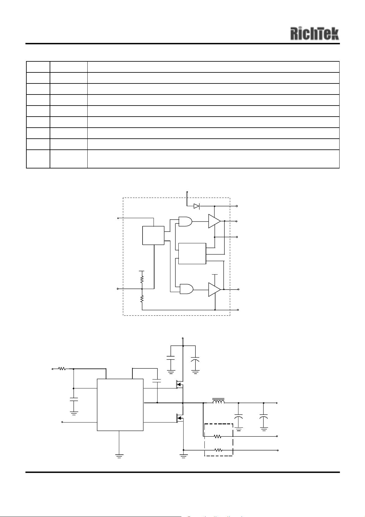
Function Block Diagram
V
CC
Internal
500K
PWM
500K
Typical Application Circuit
5V
Control
Logic
PVCC
+12V
Shootthrough
Protect
BOOT
UGATE
PHASE
V
CC
LGATE
GND
+12V
PWM
10Ω
C
13
1µF
7
3
VCC
PVCC
PWM
6
RT9600
GND
BOOT
UGATE
PHASE
LGATE
4
2
C
8
1µF
1
8
5
PHB95N03LT
C
11
1µF
Q
4
C
9
1000µF/16V
Q
3
PHB83N03LT
L3
2µH
C
15
×1500µF
R
2.4K
10
2.4K
R
13
There 2 PCB trace have to parallel and place R near to PWM IC
VCORE
C
16
×1500µF
ISEN2
ISN2
www.richtek.com DS9600-00 August, 2002
2
Page 3
Preliminary RT9600
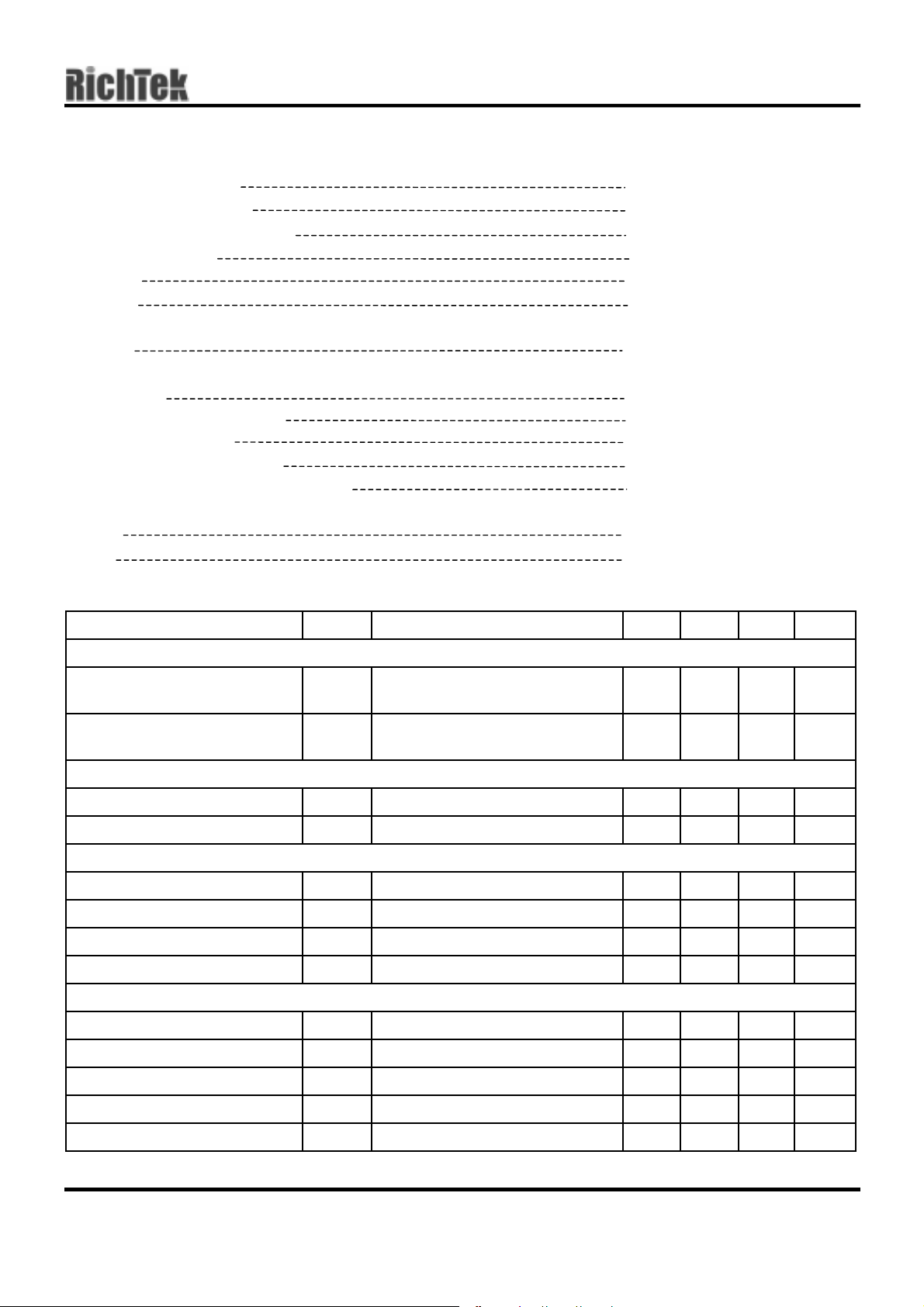
Absolute Maximum Ratings
z Supply Voltage (VCC) 15V
z Supply Voltage (PVCC) VCC + 0.3V
z BOOT Voltage (Vboot-Vphase) 15V
z PWM Input Volt age GND – 0.3V to 7V
z UGATE V
z LGATE GND – 0.3V To V
z Power Dissipation, P
@ TA = 25°C
D
SOP-8 0.625W
z Package Thermal Resistance
SOP-8, θ
z Ambient Temperature Range 0°C ~ 70°C
z Junction Temperature 0°C ~ 125°C
z Storage Temperature Range -40°C ~ 150°C
z Lead Temperature (Soldering, 10 sec.) 260°C
z EDS Level
JA
160°C /W
HBM 2KV
MM 200V
PHASE
– 0.3V to V
BOOT
PVCC
+ 0.3V
+ 0.3V
Electrical Characteristics
Parameter Symbol Test Conditions Min Typ Max Units
VCC Supply Current
f
= 250KHz, V
Bias Supply Current
Power Supply Current
I
VCC
I
PVCC
PWM
C
= 0.1µF, R
boot
f
= 500kHz, V
PWM
C
= 0.1µF, R
boot
Power-On Reset
VCC Rising Threshold 9.1 9.6 10 V
VCC Falling Threshold 7.5 8.1 8.5 V
Output
Upper Drive Source R
Upper Drive Sink R
Lower Drive Source R
Lower Drive Sink R
UGATE
UGATE
LGATE
LGATE
V
VCC
V
VCC
V
VCC
V
VCC
= 12V, V
= 12V, V
= 12V, V
= V
PVCC
PVCC
PVCC
PVCC
= 12V -- 0.75 1 Ω
PWM Input
Maximum Input Current V
= 0 or 5V -- 60 -- µA
PWM
PWM Floating Voltage VCC = 12V -- 1.9 -- V
= 12V,
PVCC
phase
PVCC
phase
= 20Ω
= 12V,
= 20Ω
-- 5.2 6 mA
-- 3.7 5 mA
= 12V -- 1.5 -- Ω
= 12V -- 1.45 2 Ω
= 12V -- 1.6 -- Ω
PWM Rising Threshold -- 3.7 -- V
PWM Falling Threshold -- 1.1 -- V
UGATE Rise Time V
PVCC
= V
= 12V, 3nF load -- 30 -- ns
VCC
To be continued
DS9600-00 August, 2002 www.richtek.com
3
Page 4
RT9600 Preliminary
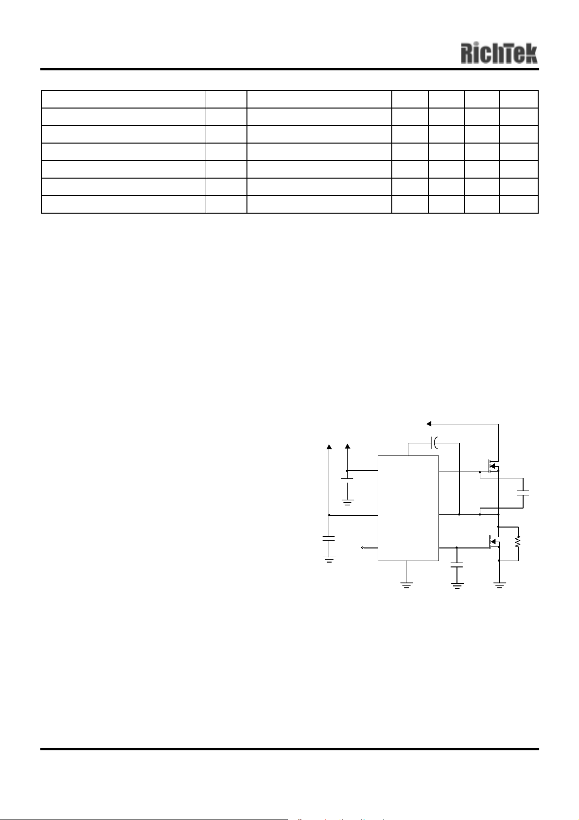
Parameter Symbol Test Conditions Min Typ Max Units
LGATE Rise Time V
UGATE Fall Time V
LGATE Fall Time V
UGATE Turn-Off Propagation Delay V
LGATE Turn-Off Propagation Delay V
PVCC
PVCC
PVCC
VCC
VCC
= V
= V
= V
= V
= V
= 12V, 3nF load -- 30 -- ns
VCC
= 12V, 3nF load -- 40 -- ns
VCC
= 12V, 3nF load -- 30 -- ns
VCC
= 12V, 3nF load -- 60 -- ns
PVCC
= 12V, 3nF load -- 45 -- ns
PVCC
Shutdown Window 1.1 -- 3.7 V
Operation Descriptions
The RT9600 is designed to drive both high side and
low side N-channel MOSFET through externally input
PWM control signal. It has power on protection
function which held UGATE and LGATE low before
V
up across the rising threshold voltage. After the
CC
initialization, the PWM signal takes the control. The
rising PWM signal first forces the LGATE signal turns
low then UGATE signal is allowed to go high just after
a non-overlapping time to avoid shoot-through
current. The falling of PWM signal first forces UGATE
Testing Conditions
The CU and CL capacitors in the test circuit are high
side and low side low capacitors. The 20Ω resistor
between PHASE and ground is implemented as the
load of the buck converter.
For output resistance, typical voltage/current
measurements are made to calculate the R
should be noted that source of both high side and low
side drivers are both current controlled current
sources, the output resistance is acquired by
interpolation.
DS(ON).
to go low. When UGATE and PHASE signal reach a
predetermined low level, LGATE signal is allowed to
turn high. The non-overlapping function is also
+12V
+12V
+12V
0.1µF
presented between UG and LG signal transient.
The PWM signal is recognized as high if above rising
threshold and as low if below falling threshold. Any
signal level in this window is considered as tri-state,
which causes turn-off of both high side and low-side
MOSFET. When PWM input is floating (not
connected), internal divider will pull the PWM to 1.9V
to give the controller a recognizable level. The
maximum sink/source capability of internal PWM
0.1µF
PWM
0.1µF
PVCC
VCC
PWM
BOOT
UGATE
RT9600
PHASE
LGATE
GND
2N7002
C
L
3nF
2N7002
reference is 60µA.
20Ω
It
C
3nF
U
The PVCC pin provides flexibility of high side
MOSFET gate drive voltage. If 8V, for example, is
Testing Circuit
applied to PVCC, then high side MOSFET gate drive
is 8V-1.5V(approximately, internal diode plus series
resistance voltage drop).
The RT9600 typically operates at frequency of
200~250KHz. A 1N4148 diode connecting PVCC and
BOOT is recommended for higher operating
frequency.
www.richtek.com DS9600-00 August, 2002
4
Page 5
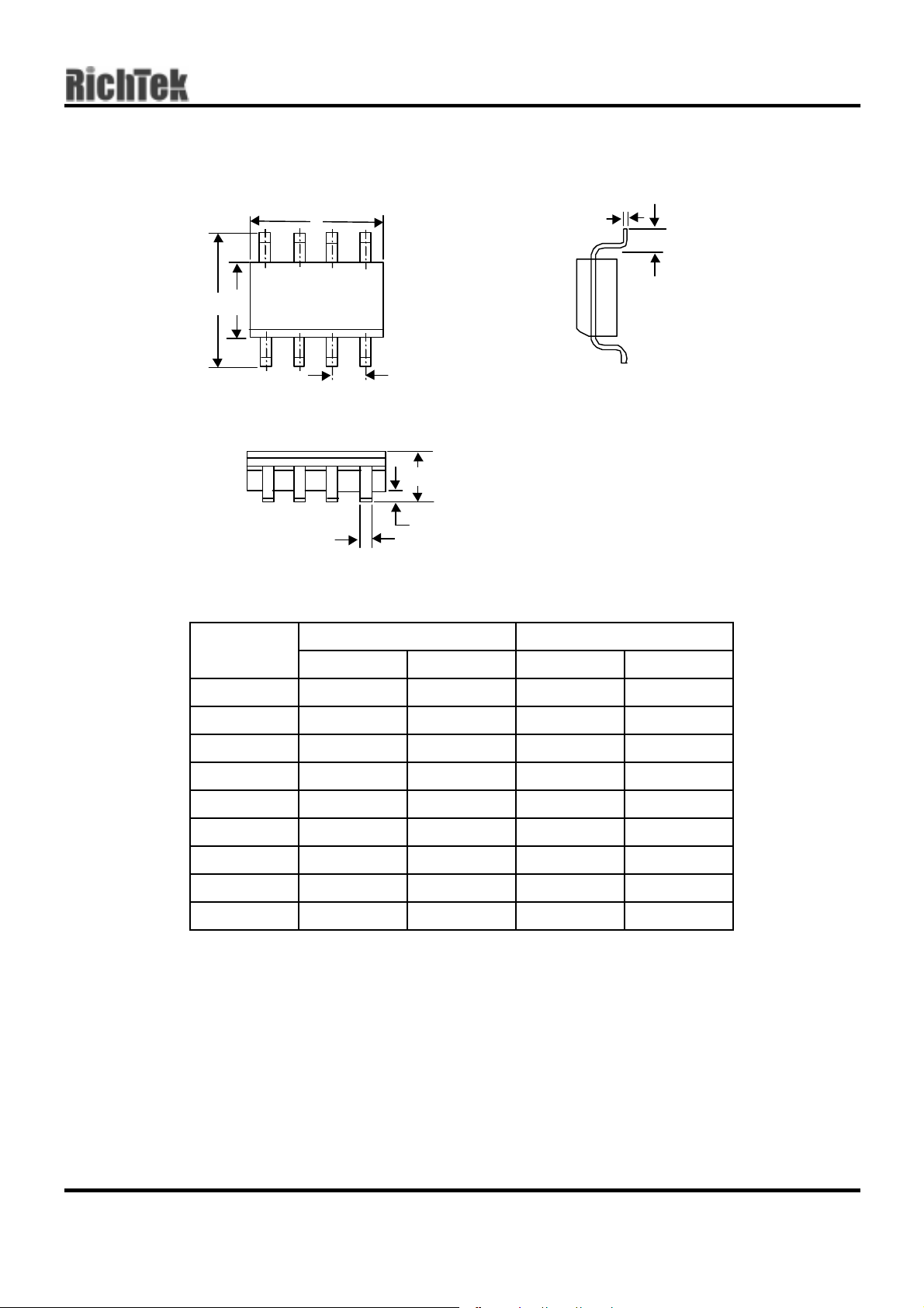
Package Information
B
J
Preliminary RT9600
H
A
M
F
C
D
I
Dimensions In Millimeters Dimensions In Inches
Symbol
Min Max Min Max
A 4.801 5.004 0.189 0.197
B 3.810 3.988 0.150 0.157
C 1.346 1.753 0.053 0.069
D 0.330 0.508 0.013 0.020
F 1.194 1.346 0.047 0.053
H 0.178 0.254 0.007 0.010
I 0.102 0.254 0.004 0.010
J 5.791 6.198 0.228 0.244
M 0.406 1.270 0.016 0.050
8–Lead SOP Plastic Package
DS9600-00 August, 2002 www.richtek.com
5
Page 6

RT9600 Preliminary
RICHTEK TECHNOLOGY CORP.
Headquarter
5F, No. 20, Taiyuen Street, Chupei City
Hsinchu, Taiwan, R.O.C.
Tel: (8863)5526789 Fax: (8863)5526611
www.richtek.com DS9600-00 August, 2002
RICHTEK TECHNOLOGY CORP.
Taipei Office (Marketing)
8F-1, No. 137, Lane 235, Paochiao Road, Hsintien City
Taipei County, Taiwan, R.O.C.
Tel: (8862)89191466 Fax: (8862)89191465
Email: [email protected]
6
 Loading...