

Page 1
Preliminary RT9238
VRM8.5 PWM and Triple Linear Power System Controller
General Description
The RT9238 is a 4-in-one power controller optimized
for high-performance microprocessor and computer
applications. The IC integrates a PWM controller,
triple linear controller as well as monitoring and
protection functions into a 28-pin SOP package. The
PWM controller regulates the microprocessor core
voltage with a synchronous buck converter. The first
linear controller supplies the computer system’s
AGTL+ 1.2V bus power. The second linear controller
provides power for the 1.5V AGP bus and the 3rd
linear controller provides 1.8V power for the chipset
core voltage and/or cache memory circuits.
The RT9238 features an Intel VRM8.5 compatible,
TTL 5-bit programmable DAC that adjusts the core
voltage from 1.090V to 1.865V in 25mV steps. The 5bit DAC has a typical ±1% tolerance. The linear
regulators provide fixed output voltages of 1.2V
(V
OUT2
), 1.5V (V
) and 1.8V (V
OUT3
OUT4
) or useradjustable with an internal 1.265V reference. All the
three linear regulators drive external N-MOSFET or
NPNs bipolar for the pass transistor.
The RT9238 monitors all the output voltages. A
power-good signal is issued when the core voltage is
within ±10% of the DAC setting and the other levels
are above their under-voltage levels. Additional buildin over-voltage protection for the core output uses the
lower MOSFET to prevent output voltage above
115% of the DAC setting. The PWM over-current
function monitors the output current using the voltage
drop across the MOSFET’s R
DS(ON)
, which
eliminates the need for a current sensing resistor .
Applications
z Motherboard Power Regulation for Computers
Features
z 4-in-one Regulated Voltages for Microprocessor
Core, AGTL+ Bus, AGP Bus Power, and
North/South Bridge Core
z Compatible with ISL6524
z Power-good Output Voltage Monitor
Switching section
z VRM8.5 TTL-Compatible 5-bit DAC
Programmable from 1.090V to 1.865V
z ±1% DAC Accuracy
z Fast Transient Response
z VRM 8.5 Voltage Droop Tuning Uses MOSFET
R
DS(ON)
z Fixed 200KHz Switching Frequency
z Adaptive Non-overlapping Gate Driver
z Over-current Monitor Uses MOSFET R
z Over-voltage Protection Uses Lower MOSFET
DS(ON)
Linear Section
z Fixed or User-adjustable Linear Regulator
Output Voltage
z MOSFET and NPN Driving Capability
z Ultra Fast Response Speed
z Under-voltage Protection
z Internal Thermal Shutdown
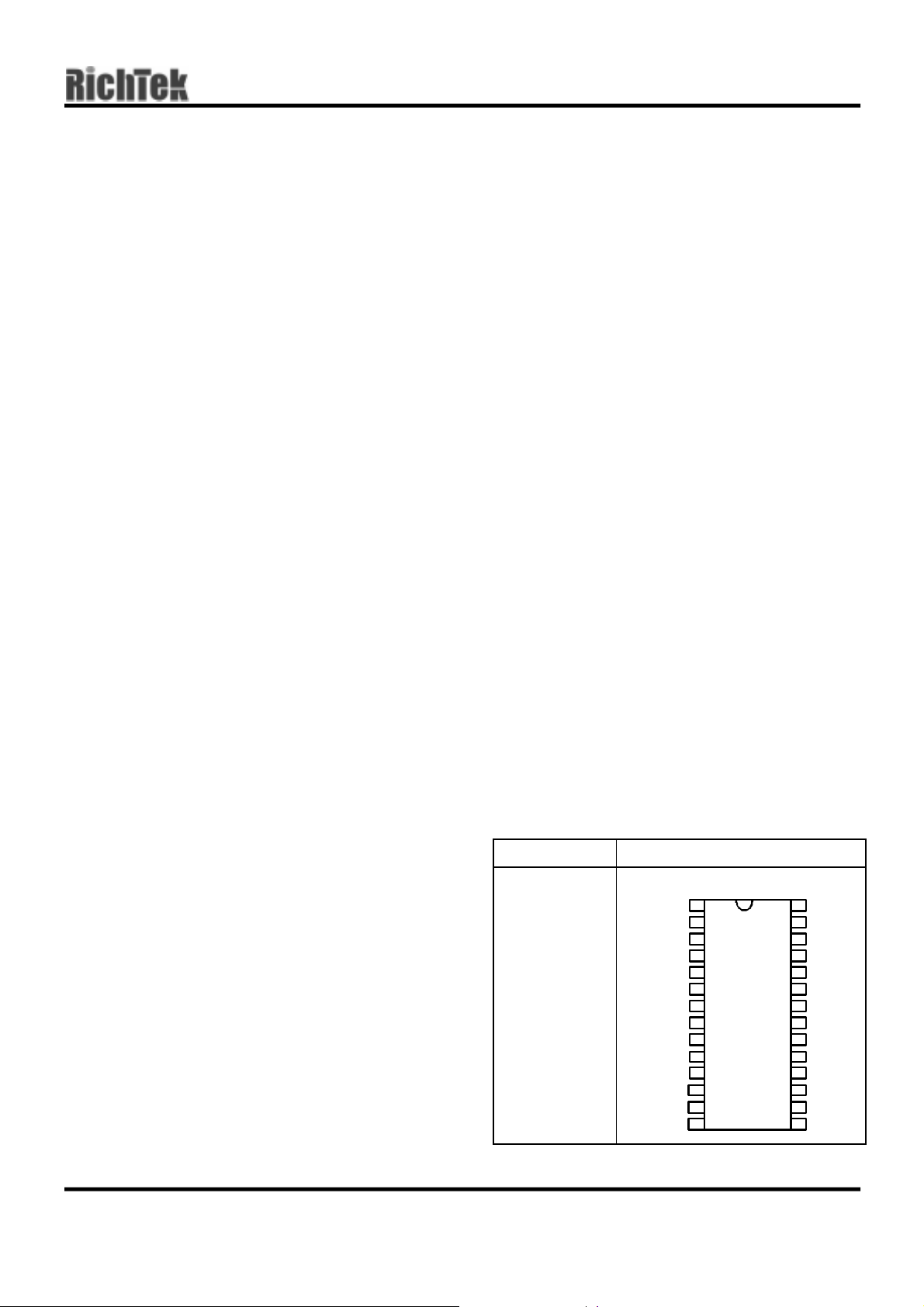
Pin Configurations
Part Number Pin Configurations
RT9238CS
DRIVE2
(Plastic SOP-28)
VID3
VID2
VID1
VID0
VID25
PGOOD
VTTPG
FAULT/VID4
VSEN2
SS24
SS13
VSEN4
TOP VIEW
1
FIX
2
3
4
5
6
7
8
9
10
11
12 17
13
14
28
27
26
25
24
23
22
21
20
19
18
16
15
VCC
UGATE1
PHASE1
LGATE1
PGND
OCSET1
FB1
VDAC
ICOMP
VSEN3
DRIVE3
GND
VAUX
DRIVE4
DS9238-01 July 2001 www.richtek.com
1
Page 2
RT9238 Preliminary
Ordering Information
RT9238
Package type
S : SOP-28
Operating temperature range
C: Commercial standard
Typical Application Circuit
L1
5V
12V
R1
10
1µH
+
C1
2000µF
VAUX
VTT
V
OUT2
1.2V
VTTPG
AGP
V
OUT3
1.5V
MCH
V
OUT4
1.8V
+
C5
1000µF
Q4
PHD3055E
+
C9
560µF
2SD1802
+
C11
560µF
PHD3055E
R6
1K
C8
1µF
Q5
C10
1µF
Q3
FIX
C6
1µF
+
11
16
C15
10µF
18
19
15
14
2
1
9
C14
1µF
VCC
FIX
DRIVE2
VSEN2
RT9238
VTTPG
VAUX
DRIVE3
VSEN3
FAULT/VID4
DRIVE4
VSEN4
GND
28
OCSET1
PGOOD
UGATE1
PHASE1
LGATE1
PGND
FB1
VDAC
ICOMP
VID25
VID0
VID1
VID2
VID3
SS24
SS13
17
Z1
15V
23
8
27
26
25
24
22
21
20
7
6
5
4
3
10
12
13
C2
1000pF
R2
1K
R6
1K
VID25
VID0
VID1
VID2
VID3
FAULT
C12
0.1µF
Q1
PHB83N03LT
L2; 1. 8 µH
Q2
PHB95N03LT
C16
10nF
C13
0.1µF
PGOOD
R3
10K
+
C3
8000µF
* C17 near the FB1 pin
as cl os e as poss i ble
VCORE
C17
1µF
C4
1µF
V
OUT1
VRM8.5
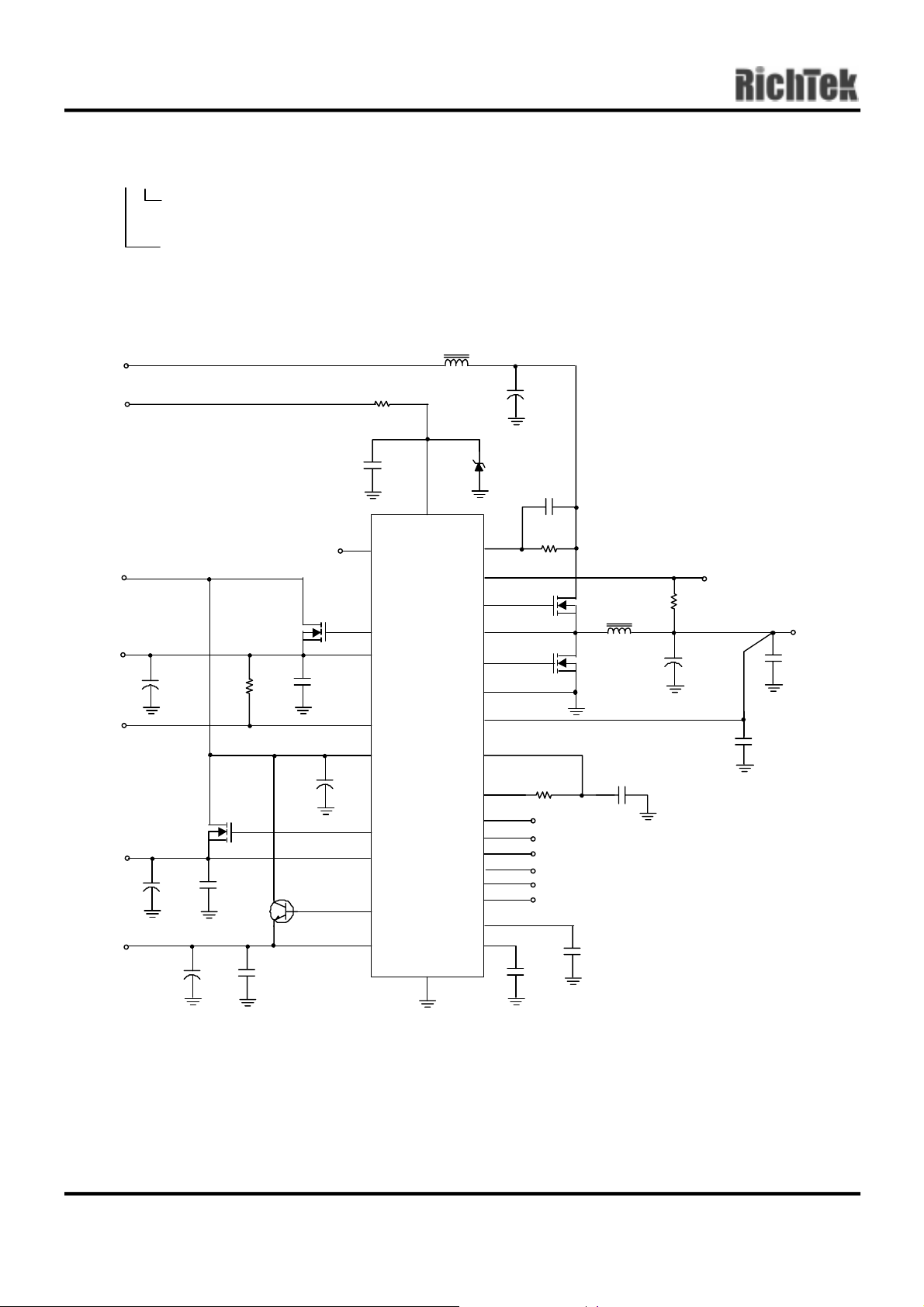
Fig.1 VRM 8.5 Power Solution
www.richtek.com DS9238-01 July 2001
2
Page 3
12V
5V
Preliminary RT9238
L1
1µH
R1
10
+
C1
2000µF
VAUX
VTT
V
OUT2
1.2V
VTTPG
AGP
V
OUT3
1.5V
MCH
V
OUT4
1.8V
+
C5
1000µF
Q4
PHD3055E
+
C9
560µF
2SD1802
+
C11
560µF
PHD3055E
R6
1K
C8
1µF
Q5
C10
1µF
Q3
FIX
C6
1µF
+
11
16
C15
10µF
18
19
15
14
2
1
9
C14
1µF
FIX
DRIVE2
VSEN2
RT9238
VTTPG
VAUX
DRIVE3
VSEN3
FAULT/VID4
DRIVE4
VSEN4
28
VCC
OCSET1
PGOOD
UGATE1
PHASE1
LGATE1
ICOMP
GND
17
PGND
FB1
VDAC
VID25
VID0
VID1
VID2
VID3
SS24
SS13
Z1
15V
23
8
27
26
25
24
22
21
20
7
6
5
4
3
10
12
13
C2
1000pF
R2
1K
R6
1K
VID25
VID0
VID1
VID2
VID3
C12
0.1µF
Q1
PHB83N03LT
L2; 1. 8 µH
Q2
PHB95N03LT
C16
10nF
MMBT3906
D1
1N4148
C13
0.1µF
Q7
R3
10K
+
C3
8000µF
R13; 47K
FAULT
PGOOD
VCORE
C4
1µF
C17
1µF
VAUX
R15
TUAL5
10K
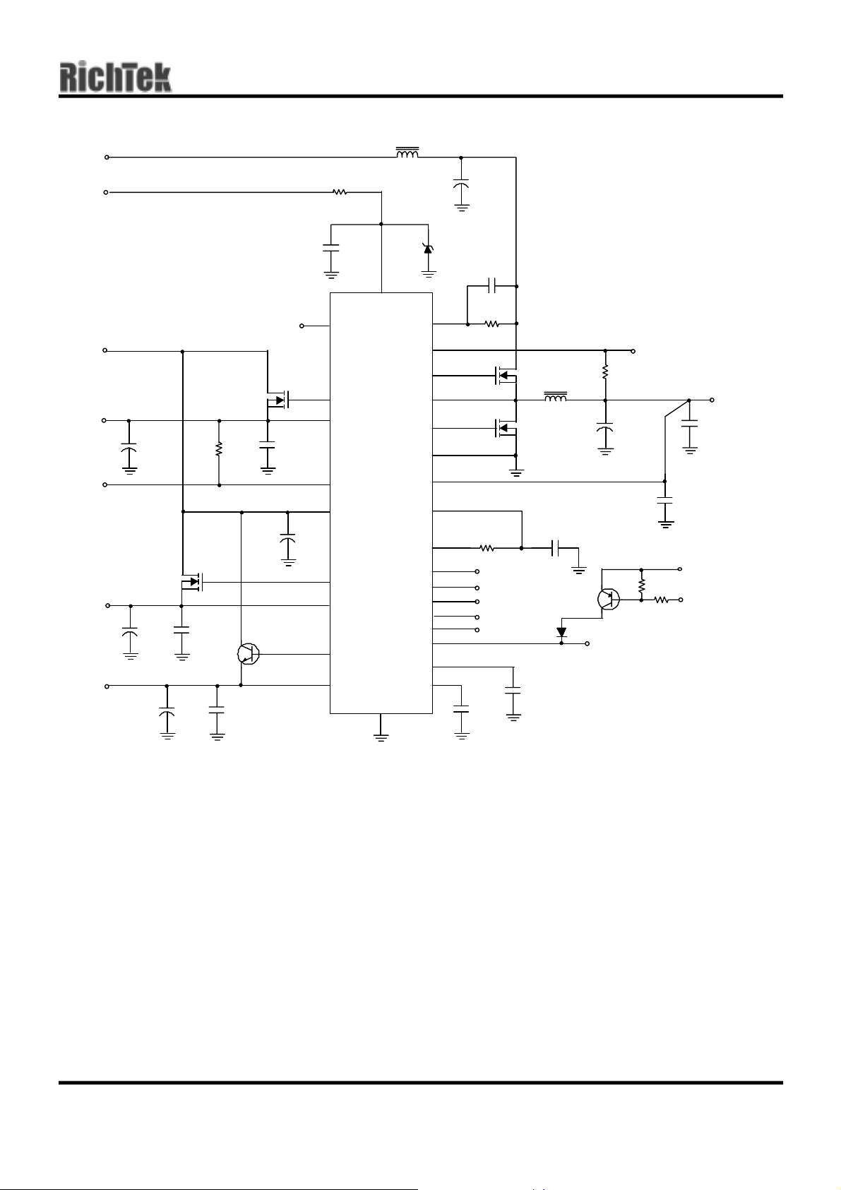
* TUAL5: Hi Tualatin
TUAL5: Lo Coppermine
V
OUT1
VRM8.5
Fig.2 VRM 8.4 & 8.5 Power Solution
DS9238-01 July 2001 www.richtek.com
3
Page 4
RT9238 Preliminary
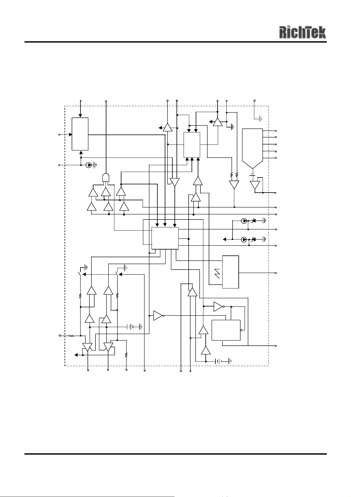
Function Block Diagram
VAUX
PGOOD
VCC
POWER-ON
RESET (POR)
200µA
_
_
_
+
×1.10
+
+
×0.90
×1.15
OV
SOFT-
PHASE1
UGATE1
VCC
DRI VE1
LGATE1
PGND
VCC
GND
VID25VID1
VID3
VDAC
FB1
SS13 SS24
VID0
VID2
ICOMP
SYN CH
DRIVE
RS
(DAC)
TTL D/A
CONVERTER
40m V
+
_
4.5V
4.5V
GATE
CONTROL
PWM
+
_
OC
LOGIC
START
& FAULT
_
PWM
COMP
+
_
+
EA1
FAULT
3K
RS
+
_
28µ A
VCC
28µA
VSEN3 OCSET
UV4
UV3
_
+
×0.75
+
_
EA3
VAU X
_
+
×0.75
+
1.26V
+
_
EA4
INHIBIT
EA2
_
+
UV2
_
+
×0.90
SETQ CLK
1.2V
+
OSCILLATOR
Q D
CLR
FAULT/VID4
VTTPG
FIX
DRIVE3
VSEN4
DRIVE4
VSEN2
DRIVE2
www.richtek.com DS9238-01 July 2001
4
Page 5
Preliminary RT9238
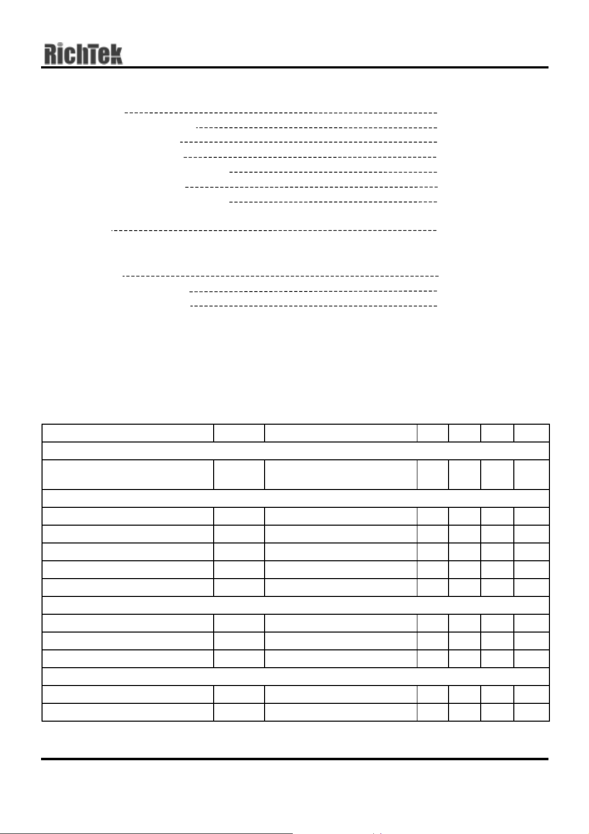
Absolute Maximum Ratings
z Supply Voltage +15V
z FAULT/VID4 and GATE Voltage GND−0.3V ~ V
z Input, Output or I/O Voltage GND−0.3V ~ 7V
z Ambient Temperature Range 0°C ~ +70°C
z Operating Junction Temperature Range 0°C ~ +125°C
z Storage Temperature Range −65°C ~ +150°C
z Lead Temperature (Soldering, 10 sec.) 300°C
z Package Thermal Resistance
SOP-28, θ
JA
60°C/W
Recommended Operating Conditions
z Supply Voltage +12V±10%
z Ambient Temperature Range 0°C to 70°C
z Junction Temperature Range 0°C to 125°C
CAUTION:
Stresses beyond the ratings specified in “Absolute Maximum Ratings” may cause permanent damage to the
device. This is a stress only rating and operation of the device at these or any other conditions above those
indicated in the operational sections of this specification is not implied.
CC
+0.3V
Electrical Characteristics
(V
= 12V, PGND = 0V, TA = 25°C, Unless otherwise specified.)
CC
Parameter Symbol Test Conditions Min Typ Max Units
VCC Supply Current
Nominal Supply Current
I
CC
UGATE1, LGATE1, DRIVE2,
DRIVE3, and DRIVE4 Open
Power-On Reset
VCC Rising Threshold
VCC Falling Threshold
Rising VAUX Threshold
VAUX Threshold Hysteresis
Rising V
OCSET1
Threshold
V
OCSET1
V
OCSET1
V
OCSET1
V
OCSET1
= 4.5V
= 4.5V
= 4.5V
= 4.5V
DAC AND Band Gap Reference
DAC (VID25-VID3) Input Low Voltage -- -- 0.8 V
DAC(VID25-VID3) Input High Voltage 2.0 -- -- V
DACOUT Voltage Accuracy VDAC + 40mV -10 -- +20 mV
Oscillator
-- 10 -- mA
6.5 -- 9.5 V
6--9 V
-- 1.5 -- V
-- 0.2 -- V
-- 1.25 -- V
Free Running Frequency 180 200 225 KHz
Ramp Amplitude
∆ V
OSC
-- 1.9 --
V
P-P
To be continued
DS9238-01 July 2001 www.richtek.com
5
Page 6

RT9238 Preliminary
Parameter Symbol Test Conditions Min Typ Max Units
Linear Regulators (V
OUT2
, V
OUT3
, and V
OUT4
)
VSEN3,4 Voltage Regulation VREG2,3,4 FIX = 0V 1.240 1.265 1.290 V
VSEN2 Regulation Voltage VREG2 1.180 1.200 1.240 V
VSEN3 Regulation Voltage VREG3 FIX = open 1.455 1.500 1.545 V
VSEN3 Bias Current IBVSEN3 FIX = open -- 260 --
µA
VSEN4 Regulation Voltage VREG4 FIX = open 1.746 1.800 1.854 V
VSEN4 Bias Current IBVSEN4 FIX = open -- 350 -Under-Voltage Level
(All Linears) (VSEN/VREG)
Under-Voltage Hysteresis
(All Linears) (VSEN/VREG)
VSEN3,4 Rising -- 75 --
VSEN3,4 Falling -- 100 --
Output Drive Current (All Linears) VAUX – VDRIVER2,3,4 > 0.6V 20 40 --
µA
%
mV
mA
Synchronous PWM Controller Error Amplifier
DC Gain -- 65 --
dB
PWM Controller Gate Driver
UGATE Source
UGATE Sink
LGATE Source
LGATE Sink
UGATE1
R
UGATE1VUGATE1
I
LGATE1
R
LGATE1
VCC-V
VCC = 12V, V
V
LGATE1
R
VCC = 12V
UGATE1
= 1V
= 1V
= 1V
LGATE1
= 2V
-- 4 7
-- 3 7
-- 1 --
-- 2 6
Ω
Ω
Ω
Protection
A
V
Over-Voltage Trip
OUT1
FAULT Souring Current
OCSET1 Current Source
Soft-Start Current
I
OCSET
I
SS13,24
FB1 Rising 112 118 125
V
FAULT
V
OCSET1
V
SS13,SS24
= 8V
= 4.5V
= 2V
510--
170 200 230
-- 28 --
%
mA
µA
µA
Power Good
V
Upper Threshold
OUT1
V
Under Voltage
OUT1
V
Hysteresis (FB1/DACOUT)
OUT1
FB1 Rising 108 -- 112
FB1 Rising 87 -- 92
Upper/Lower Threshold -- 2 -VTTPG Upper Threshold VSEN2 Rising -- 1.08 -VTTPG Delay Threshold SS13 Rising -- 1.25 -VTTPG Voltage Low
PGOOD Voltage Low
www.richtek.com DS9238-01 July 2001
V
VTTPG
V
PGOODIPGOOD
I
VTTPG
= -4mA
= -4mA
-- -- 0.5
-- -- 0.5
%
%
%
V
V
V
V
6
Page 7

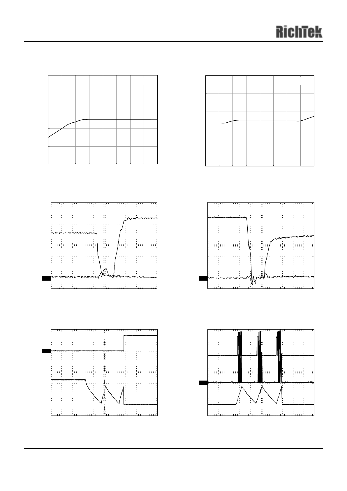
Typical Operating Charateristics
Preliminary RT9238
Frequency vs. V
205
203
201
199
CC
Frequency (KHz)
197
195
10 11 12 13 14
V
(Volt)
CC
V
Line Regulation
OUT1
1.00
0.60
TA = 25°C
= 25°C
A
I
V
OUT2,3,4
OCSET1
205
203
201
(uA )
199
OCSET1
I
197
195
10 11 12 13 14
1
0.6
vs. V
CC
(Volt)
V
CC
Line Regulation
T
A
TA = 25°CT
= 25°C
0.20
-0.20
Percentage (%)
-0.60
-1.00
10 11 12 13 14
(Volt)
V
CC
Freq u en c y vs. Temperatu r e
205
203
201
199
Frequency (KHz)
197
VCC = 12V
0.2
-0.2
Percen tage (%)
-0.6
-1
10 11 12 13 14
(Volt)
V
CC
300
275
250
I
OCSET1
vs. Temperature
(uA)
225
OCSENT1
I
200
175
VCC = 12V
195
-40 -20 0 20 40 60 80 100 120
Temperature
(°C)
150
-40-200 20406080100120
Temperature
(°C)
DS9238-01 July 2001 www.richtek.com
7
Page 8
RT9238 Preliminary
T
T
1 >2 >
>2 >
TTT
1 >
2 >
3 >
V
vs. T emper a tu r e
1
0.6
0.2
-0.2
OUT1
VCC = 12V
Percen tage (%)
-0.6
-1
-40-200 20406080100120
Temperature
(°C)
Dead Time
UGATE1
LGATE1
0.6
0.2
-0.2
V
OUT2,3,4
1
vs. T emperatu r e
VCC = 12V
Percen t a ge (%)
-0.6
-1
-40 -20 0 20 40 60 80 100 120
Temperature
(°C)
Dead Time
UGATE1
LGATE1
1 >2 >
1) Ch 1: 2 Volt 50 n s
2) Ch 2: 2 Volt 50 n s
Time
V
OUT2,3,4
1
1) Ch 1: 5 Volt 25 ms
2) Ch 2: 2 Volt 25 ms
Time
Short
T
T
FAULT
SS13,24
T
1) Ch 1: 2 Volt 50 ns
2) Ch 2: 2 Volt 50 ns
T
Time
V
Short
OUT1
UGATE1
LGATE1
SS13,24
1) Ch 1: 5 Volt 25 ms
2) Ch 2: 2 Volt 25 ms
3) Ref A: 5 Volt 25 ms
Time
www.richtek.com DS9238-01 July 2001
8
Page 9

Functional Pin Description
Preliminary RT9238
DRIVE2 (Pin 1)
Connect this pin to the gate of an external MOSEFT.
This pin provides the drive for the VTT (V
OUT2
regulator’s pass transistor.
FIX (Pin 2)
Grounding this pin bypasses the internal resistor
dividers that set the voltage of the 1.5V and 1.8V
linear regulators. This way, the output voltage of the
two regulators can be adjusted from 1.26V up to the
input voltage (+3.3V or +5V) by way of an external
resistor divider corrected at the corresponding VSEN
pin. The new output voltage set by the external
resistor divider can be determined using the following
formula:
R
V
= 1.265V x (1+
OUT
Where R
is the resistor connected from VSEN to
OUT
the output of the regulator, and R
R
OUT
GND
)
is the resistor
GND
connected from VSEN to ground. Left open, this pin
is pulled high enabling fixed output voltage operation.
VID25, VID0, VID1, VID2, VID3 (Pin 7, 6, 5, 4, and 3)
VID3-25 are TTL-compatible the input pins to the 5bit DAC. The state logic of these five pins program
the internal voltage reference, DACOUT. The level of
DACOUT sets the microprocessor core converter
output voltage, as well as the corresponding PGOOD
and OVP thresholds. Table 1 specifies the DACOUT
voltage of 32 combinations of VID levels.
PGOOD (Pin 8)
PGOOD is an open collector output used to indicate
the status of the PWM converter output voltage. This
pin is pulled low when the synchronous regulator
output is not within ±10% of the DACOUT reference
voltage, or when any of the other outputs are below
their under-voltage thresholds.
VTTPG (Pin 9)
VTTPG is an open collector output used to indicate
the status of the VTT (V
)
regulator output
OUT2
voltage. This pin is pulled low when the output
voltage is below 1.08V under-voltage threshold or
when SS13 pin is below 1.25V.
)
FAULT/VID4 (Pin 10)
This pin provides two combined functions. One is
fault condition indicator, the other is VID4 for
VRM8.4 DAC (see the Table I). Pull up this pin up to
over 2V, it act like the VID4 of VRM8.4. When this
pin is pulled high, the DACOUT provide
1.890V~2.090V output voltages.
Nominally, the voltage at this pin is pulled low by a
internal 47kΩ, in the event of an over-voltage or
over-current condition, this pin is internally pulled to
about 8V (VCC = 12V).
VSEN2 (Pin 11)
Connect this pin to the output of the VTT (V
OUT2
)
linear regulator. This pin is also monitored for undervoltage events.
SS24 (Pin 12)
Connect a capacitor from this pin to ground. This
capacitor, along with an internal 28µA (V
SS24
>1V)
current source, sets the soft-start interval of the
V
regulator. Pulling this pin below 0.8V induces
OUT2
a chip reset and shutdown.
SS13 (Pin 13)
Connect a capacitor from this pin to ground. This
capacitor, along with an internal 28µA (V
SS13
>1V)
current source, sets the soft-start interval of the
synchronous PWM converter (V
regulator (V
). A VTTPG high signal is also
OUT3
) and the AGP
OUT1
delayed by the time interval required by the charging
of this capacitor from 0V to 1.25V.
VSEN4 (Pin 14)
Connect this pin to the output of the 1.8V regulator.
This pin is monitored for under-voltage events.
DRIVE4 (Pin 15)
Connect this pin to the gate of an external MOSEFT.
This pin provides the drive for the 1.8V regulator’s
pass transistor.
DS9238-01 July 2001 www.richtek.com
9
Page 10

RT9238 Preliminary
V AUX (Pin 16)
This pin provides boost current for the three linear
regulator output drives in the event bipolar NPN
transistors (instead of N-channel MOSFETs) are
employed as pass elements. The voltage at this pin
is monitored for power-on reset (POR) purpose.
GND (Pin 17)
Signal ground for the IC. All voltage levels are
measured with respect to this pin.
An over-current trip cycles the soft-start function. The
voltage at this pin is monitored for power-on reset
(POR) purpose and pulling this pin low with an open
drain device will shut down the IC.
PGND (Pin 24)
This is the power ground of UGATE1&LGATE1. Tie
the synchronous PWM converter’s lower MOSFET
source to this pin.
DRIVE3 (Pin 18)
Connect this pin to the gate of an external MOSEFT.
This pin provides the drive for the 1.5V regulator’s
pass transistor.
VSEN3 (Pin 19)
Connect this pin to the output of the 1.5V linear
regulator. This pin is monitored for under-voltage
events.
ICOMP (Pin 20)
This pin is non-inverting input of the PWM error
amplifier. It determine the V
voltage. Connect a
OUT1
resistor (RF) to VDAC pin. A sense current of lower
MOSFET is fed to this pin to pull low the DACOUT
voltage. (see VDAC)
VDAC (Pin 21)
This pin is internal DAC buffer output. Connect a
resistor(RF) from this pin to ICOMP pin. The resistor
provide a voltage drop rated from lower MOSFET
turn on voltage drop. A sample hold circuit sense the
voltage drop of lower MOSFET(I
x RDSON ) when
L
LGATE1 turn on. The ratio is :
(I
L x R
DSON
)
x RF/3k
LGATE1 (Pin 25)
Connect LGATE1 to the PWM converter’s lower
MOSFET gate. This pin provides the gate drive for
the lower MOSFET.
PHASE1 (Pin 26)
This pin is used to monitor the voltage drop across
the upper MOSFET for over-current protection. This
pin is also used to sense lower MOSFET voltage
drop for V
OUT1 voltage droop tuning.
UGATE1 (Pin 27)
Connect UGATE1 pin to the PWM converter ’s upper
MOSFET gate. This pin provides the gate drive for
the upper MOSFET.
VCC (Pin 28)
Provide a 12V supply voltage for the IC to this pin.
This pin also provides the gate bias charge for all the
MOSFETs controlled by the IC. The voltage at this
pin monitored for power-on reset (POR) purpose
.
FB1 (Pin 22)
This pin is connected to the PWM converter’s output
voltage. This pin also connects to internal PWM error
amplifier inverting input and power good monitor.
OCSET1 (Pin 23)
Connect a resistor from this pin to the drain of the
respective upper MOSFET. This resistor, an internal
200µA current source, and the upper MOSFET onresistance set the converter over-current trip point.
www.richtek.com DS9238-01 July 2001
10
Page 11

Preliminary RT9238
Functional Description
Operation
The RT9238 monitors and precisely controls 4 output
voltage levels (Refer to Figures 1, 2, and function
block). It is designed for microprocessor computer
applications with 3.3V, 5V, and 12V bias input from
an ATX power supply. The IC has one PWM and
three linear controllers. The PWM controller is
designed to regulate the microprocessor core voltage
(V
and Q2) in a synchronous-rectified buck converter
configuration and regulates the core voltage to a level
programmed by the 5-bit digital-to-analog converter
(DAC). The first linear controller (EA2) is designed to
provide the AGTL+ bus voltage (V
MOSFET (Q3) pass element to regulate the output
voltage to a level of 1.2V. The remaining two linear
controllers (EA3 and EA4) supply the 1.5V advanced
graphics port (AGP) bus power (V
chipset core power (V
Initialization
The RT9238 automatically initializes in ATX-based
systems upon receipt of input power. The Power-On
Reset (POR) function continually monitors the input
supply voltages. The POR monitors the bias voltage
(+12V
at the OCSET pin, and the 3.3V input voltage
(+3.3V
OCSET is equal to +5V
(see over-current protection). The POR function
initiates soft-start operation after all supply voltages
exceed their POR thresholds.
). The PWM controller drives 2 MOSFETs (Q1
OUT1
) by driving a
OUT2
) and the 1.8V
OUT3
).
OUT4
) at the VCC pin, the 5V input voltage (+5VIN)
IN
) at the VAUX pin. The normal level on
IN
less a fixed voltage drop
IN
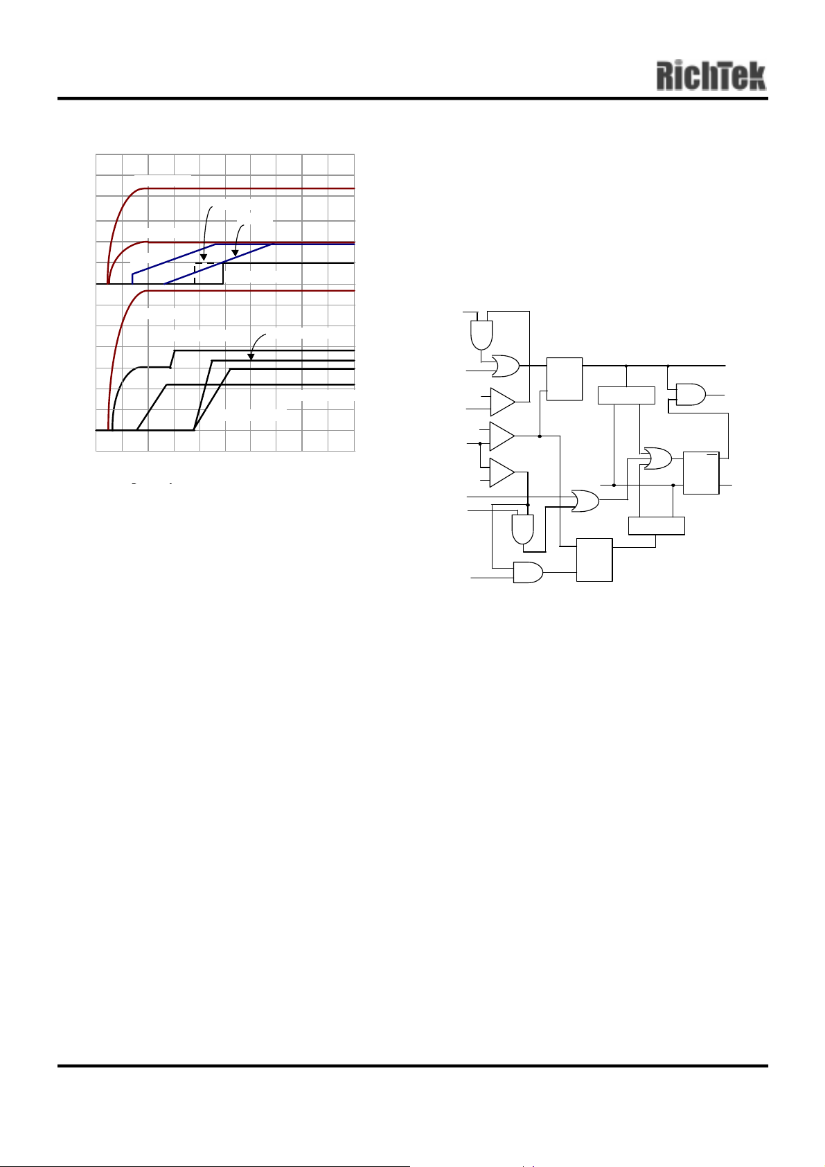
input supplies ramp up. Immediately following, OUT4
is also ramped up, lagging the ATX 3.3V by about
1.8V. At time T1, the POR function initiates the SS24
soft-start sequence. Initially, the voltage on the SS24
pin rapidly increases to approximately 1V (this
minimizes the soft-start interval). Then, an internal
28µA current source charges an external capacitor
(C
) on the SS24 pin to about 4.5V. As the SS24
SS24
voltage increases, the EA2 error amplifier drives Q3
to provide a smooth transition to the final set voltage.
The OUT4 reference (clamped to SS24) increasing
past the intermediary level, established based on the
ATX 3.3V presence at the VAUX pin, brings the
output in regulation soon after T2.
As OUT2 increases past the 90% power-good level,
the second soft-start (SS13) is released. Between T2
and T3, the SS13 pin voltage ramps from 0V to the
valley of the oscillator’s triangle wave (at 1.25V).
Contingent upon OUT2 remaining above 1.08V, the
first PWM pulse on PHASE1 triggers the VTTPG pin
to go high. The oscillator’s triangular wave form is
compared to the clamped error amplifier output
voltage. As the SS13 pin voltage increases, the
pulse-width on the PHASE1 pin increases, bringing
the OUT1 output within regulation limits. Similarly, the
SS13 voltage clamps the reference voltage for OUT3,
enabling a controlled output voltage ramp-up. At time
T4, all output voltages are within power-good limits,
situation reported by the PGOOD pin going high.
Soft-Start
The 1.8V supply designed to power the chipset
(OUT4), cannot lag the ATX 3.3V by more than 2V, at
any time. To meet this special requirement, the linear
block controlling this output operates independently
of the chip’s power-on reset. Thus, DRIVE4 is driven
to raise the OUT4 voltage before the input supplies
reach their POR levels. As seen in Fig.3, at time T0
The T2 to T3 time interval is dependent upon the
value of C
. The same capacitor is also
SS13
responsible for the ramp-up time of the OUT1 and
OUT3 voltages. If selecting a different capacitor then
recommended in the circuit application literature,
consider the effects the different value will have on
the ramp-up time and inrush currents of the OUT1
and OUT3 outputs.
the power is turned on and the
DS9238-01 July 2001 www.richtek.com
11
Page 12
RT9238 Preliminary
VSEN4) is ignored until the respective UP signal
ATX12V
10V
0V
3.0V
0V
T0 T3
ATX5V
SS24
ATX3.3V
V
OUT4
T1 T2 T4T5
VTTPG
(1.8V)
V
TIME
SS13
PGOOD
OUT3
(1.5V)
V
OUT1
V
OUT2
(1.65V)
(1.2V)
Fig.3 Soft-start Interval
Fault Protection
All four outputs are monitored and protected against
extreme overload. The chip’s response to an output
overload is selective, depending on the faulting
output.
goes high. This allows V
without fault at start-up. Following an over-current
event (OC1, UV2, or UV3 event), bringing the SS24
pin below 0.8V resets the over-current latch and
generates a soft-started ramp-up of the outputs 1, 2,
and 3.
UV3
OC1
SS13
SS24
OV
UV4
UV2
and V
OUT3
SS13UP
OC
LATCH
S Q
SS24UP
R
COUNTER
POR
OC
LATCH
R
S Q
R
COUNTER
0.8V
_
4V
+
+
_
+
_
4V
Fig.4 Fault Logic-simplified Schematic
to increase
OUT4
IN HIB I T 1,2,3
FAULT
LATCH
S Q
R Q
R
SSDOWN
FAULT
An over-voltage on V
outputs 1, 2, and 3, and latches the IC off. An undervoltage on V
output latches the IC off. A single
OUT4
over-current event on output 1, or an under-voltage
event on output 2 or 3, increments the respective
fault counters and triggers a shutdown of outputs 1,
2, and 3, followed by a soft-start re-start. After three
consecutive fault events on either counter, the chip is
latched off. Removal of bias power resets both the
fault latch and the counters. Both counters are also
reset by a successful start-up of all the outputs.
output (FB1) disables
OUT1
OUT1 Over-Voltage Protection
During operation, a short across the synchronous
PWM upper MOSFET (Q1) causes V
OUT1
to
increase. When the output exceeds the over-voltage
threshold of 115% of DACOUT, the over-voltage
comparator trips to set the fault latch and turns the
lower MOSFET (Q2) on. This blows the input fuse
and reduces V
OUT1
.
A separate over-voltage circuit provides protection
during the initial application of power. For voltages on
the VCC pin below the power-on reset (and above
Fig.3 shows a simplified schematic of the fault logic.
The over-current latches are set dependent upon the
states of the over-current (OC1), output 2 and 3
~4V), the output level is monitored for voltages above
1.3V. Should FB1 exceed this level, the lower
MOSFET, Q2, is driven on.
under-voltage (UV2, UV3) and the soft-start signals
(SS13, SS24). Window comparators monitor the SS
pins and indicate when the respective C
pins are
SS
fully charged to above 4.0V (UP signals). An under-
Over-Current Protection
All outputs are protected against excessive overcurrents. The PWM controller uses the upper
voltage on either linear output (VSEN2, VSEN3, or
www.richtek.com DS9238-01 July 2001
12
Page 13
Preliminary RT9238
MOSFET’s on-resistance, R
to monitor the
DS(ON)
current for protection against a shorted output. All
linear regulators monitor their respective VSEN pins
for under-voltage to protect against excessive
currents.
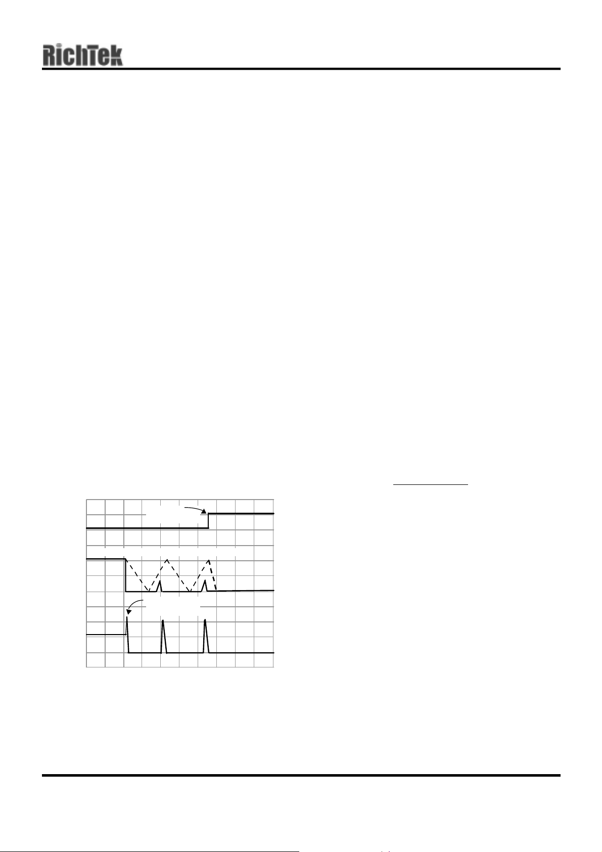
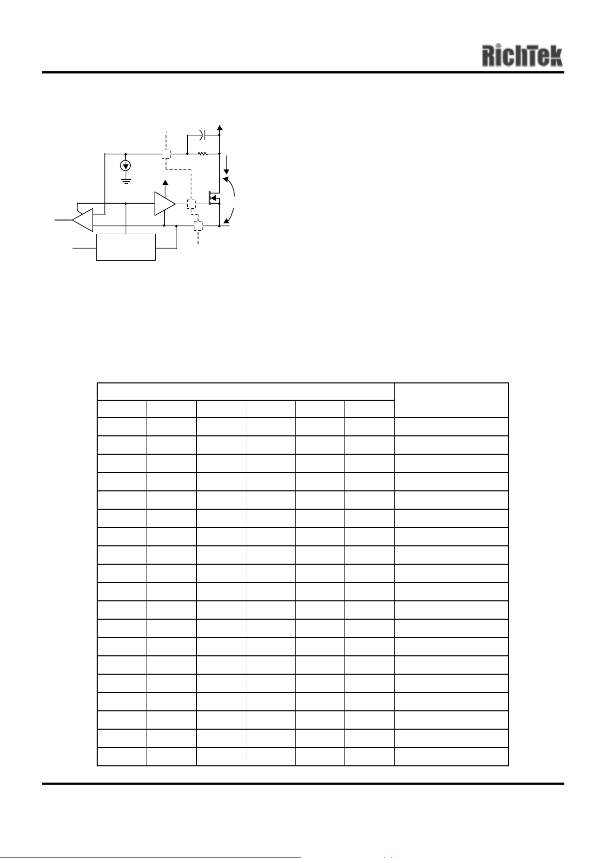
Fig.5 illustrates the over-current protection with an
overload on OUT1. The overload is applied at T0 and
the current increases through the inductor (L
OUT1
). At
time T1, the OC1 comparator trips when the voltage
across Q1 (i
programmed by R
D•RDS(ON)
OCSET
and 3, discharges the soft-start capacitor C
) exceeds the level
. This inhibits outputs 1, 2,
with
SS24
28µA current sink, and increments the counter. Softstart capacitor C
is quickly discharged. C
SS13
SS13
starts ramping up at T2 and initiates a new soft-start
cycle. With OUT2 still overloaded, the inductor
current increases to trip the over-current comparator.
Again, this inhibits the outputs, but the C
SS24
softstart voltage continues increasing to above 4.0V
before discharging. Soft-start capacitor C
SS13
is,
again, quickly discharged. The counter increments to
2. The soft-start cycle repeats at T3 and trips the
over-current comparator. The SS24 pin voltage
increases to above 4.0V at T4 and the counter
increments to 3. This sets the fault latch to disable
the converter.
FAULT
REPORTED
OVERLOAD
APPLIED
T3T4
TIME
24
SS
10V
0V
FAULT/RT
COUNT = 1 COUNT = 2 COUNT = 3
4V
13
2V
SS
0V
0A
INDUCTOR CURRENT
T0T1 T2
Fig.5 Over-current Operation
The three linear controllers monitor their respective
VSEN pins for under-voltage. Should excessive
currents cause VSEN3 or VSEN4 to fall below the
linear under-voltage threshold, the respective UV
signals set the OC latch or the FAULT latch,
providing respective C
charged. Blanking the UV signals during the C
capacitors are fully
SS
SS
charge interval allows the linear outputs to build
above the under-voltage threshold during normal
operation. Cycling the bias input power off then on
resets the counter and the fault latch.
An external resistor (R
) programs the over-
OCSET
current trip level for the PWM converter. As shown in
Fig.6, the internal 200µA current sink (I
develops a voltage across R
referenced to V
. The DRIVE signal enables the
IN
OCSET
(V
) that is
SET
OCSET
over-current comparator (OC). When the voltage
across the upper MOSFET (V
DS(ON)
) exceeds V
SET
the over-current comparator trips to set the overcurrent latch. Both V
V
and a small capacitor across R
IN
V
track the variations of V
OCSET
and VDS are referenced to
SET
OCSET
due to MOSFET
IN
helps
switching. The over-current function will trip at a peak
inductor current (I
I
=
PEAK
The OC trip point varies with MOSFET’s R
) determined by:
PEAK
RI
×
R
OCSETOCSET
)ON(DS
DS(ON)
temperature variations. To avoid over-current tripping
in the normal operating load range, determine the
ROCSET resistor value from the equation above
with:
1. The maximum R
at the highest junction
DS(ON)
temperature
2. The minimum I
3. Determine I
PEAK
from the specification table
OCSET
for I
PEAK
> I
OUT(MAX)
+ (∆I)/ 2,
where ∆I is the output inductor ripple current.
For an equation for the ripple current see the section
under component guidelines titled ‘Output Inductor
Selection’.
)
,
DS9238-01 July 2001 www.richtek.com
13
Page 14
RT9238 Preliminary
OVE R- CURRENT TRI P :
V
> V
DS
SET
iD
OC
×R
PWM
DS(ON)
+
_
> I
OCSET
OCSET
I
OCSET
200µA
DRIVE
GATE
CONTROL
× R
OCSET
VCC
R
OCSET
V
UGATE
PHASE
V
PHASE
V
OCSET
SET+
= V
= V
IN
V
= +5V
IN
i
D
V
DS+
- V
DS
- V
IN
SET
Fig.6 Current Limiting Setting
OUT1 Voltage Program
The output voltage of the PWM converter is
programmed to discrete levels between 1.090V and
Table 1. VOUT1 Voltage Program
1.865V which are shifted high 40mV from 1.050V to
1.825V for voltage droop gap tuning. This output
(OUT1) is designed to supply the core voltage of
Intel’s advanced microprocessors. The voltage
identification (VID) pins program an internal voltage
reference (DACOUT) with a TTL-compatible 5-bit
digital-to-analog converter (DAC). The level of
DACOUT also sets the PGOOD and OVP thresholds.
Table 1 specifies the DACOUT voltage for the
different combinations of connections on the VID
pins. The VID pins can be left open for a logic 1 input,
since they are internally pulled to the VAUX pin
through 5KΩ resistors. Changing the VID inputs
during operation is not recommended and could
toggle the PGOOD signal and exercise the overvoltage protection. The output voltage program is
Intel VRM8.5 compatible.
Pin Name
VID4 VID3 VID2 VID1 VID0 VID25
001000
001001
000110
000111
000100
000101
000010
000011
000000
000001
011110
011111
011100
011101
011010
Normal OUT1 Voltage
DACOUT
1.050+40mV=1.090
1.075+40mV=1.115
1.100+40mV=1.140
1.125+40mV=1.165
1.150+40mV=1.190
1.175+40mV=1.215
1.200+40mV=1.240
1.225+40mV=1.265
1.250+40mV=1.290
1.275+40mV=1.315
1.300+40mV=1.340
1.325+40mV=1.365
1.350+40mV=1.390
1.375+40mV=1.415
1.400+40mV=1.440
011011
011000
011001
010110
1.425+40mV=1.465
1.450+40mV=1.490
1.475+40mV=1.515
1.500+40mV=1.540
To be continued
www.richtek.com DS9238-01 July 2001
14
Page 15

Preliminary RT9238
Pin Name
VID4 VID3 VID2 VID1 VID0 VID25
010111
010100
010101
010010
010011
010000
010001
001110
001111
001100
001101
001010
001011
1010001.850+40mV=1.890
1001101.900+40mV=1.940
Normal OUT1 Voltage
DACOUT
1.525+40mV=1.565
1.550+40mV=1.590
1.575+40mV=1.615
1.600+40mV=1.640
1.625+40mV=1.665
1.650+40mV=1.690
1.675+40mV=1.715
1.700+40mV=1.740
1.725+40mV=1.765
1.750+40mV=1.790
1.775+40mV=1.815
1.800+40mV=1.840
1.825+40mV=1.865
1001001.950+40mV=1.990
1000102.000+40mV=2.040
1000002.050+40mV=2.090
Notes: 0=connect to GND, 1=open or connect to 3.3V through pull up resistor
Application Guidelines
Soft-Start Interval
Initially, the soft-start function clamps the error
amplifier’s output of the PWM converter. This
generates PHASE pulses of increasing width that
charge the output capacitor(s). The resulting output
voltages start-up as shown in Fig.3.
The soft-start function controls the output voltage rate
of rise to limit the current surge at start-up. The softstart interval and the surge current are programmed
by the soft-start capacitor, C
faster soft-start interval increases the peak surge
current. Using the recommended 0.1µF soft start
capacitors ensure all output voltages ramp up to their
set values in a quick and controlled fashion, while
meeting the system timing requirements.
. Programming a
SS
Shutdown
The PWM output does not switch until the soft-start
voltage (V
voltage. Additionally, the reference on each linear’s
amplifier is clamped to the soft-start voltage. Holding
the SS24 pin low (with an open drain or open
collector signal) turns off regulators 1, 2 and 3.
Regulator 4 (MCH) will simply drop its output to the
intermediate soft-start level. This output is not
allowed to violate the 2V maximum potential gap to
the ATX 3.3V output.
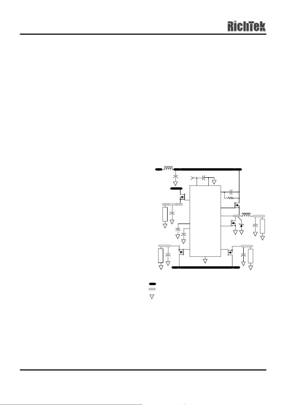
Layout Considerations
MOSFETs switch very fast and efficiently. The speed
with which the current transitions from one device to
another causes voltage spikes across the
interconnecting impedances and parasitic ci rcuit
) exceeds the oscillator’s valley
SS13
DS9238-01 July 2001 www.richtek.com
15
Page 16
RT9238 Preliminary
elements. The voltage spikes can degrade efficiency,
radiate noise into the circuit, and lead to device overvoltage stress. Careful component layout and printed
circuit design minimizes the voltage spikes in the
converter. Consider, as an example, the turn-off
transition of the upper MOSFET. Prior to turn-off, the
upper MOSFET was carrying the full load current.
During the turn-off, current stops flowing in the upper
MOSFET and is picked up by the lower MOSFET or
Schottky diode. Any inductance in the switched
current path generates a large voltage spike during
the switching interval. Careful component selection,
tight layout of the critical components, and short,
wide circuit traces minimize the magnitude of voltage
spikes.
There are two sets of critical components in a DC-DC
converter using an RT9238 controller. The switching
power components are the most critical because they
switch large amounts of energy, and as such, they
tend to generate equally large amounts of noise. The
critical small signal components are those connected
to sensitive nodes or those supplying critical bypass
current.
The power components and the controller IC should
be placed first. Locate the input capacitors, especially
the high-frequency ceramic de-coupling capacitors,
close to the power switches. Locate the output
inductor and output capacitors between the
MOSFETs and the load. Locate the PWM controller
close to the MOSFETs.
component ground connections with vias to this layer.
Dedicate another solid layer as a power plane and
break this plane into smaller islands of common
voltage levels. The power plane should support the
input power and output power nodes. Use copper
filled polygons on the top and bottom circuit layers for
the PHASE node, but do not unnecessarily oversize
this particular island. Since the PHASE node is
subject to very high dV/dt voltages, the stray
capacitor formed between these island and the
surrounding circuitry will tend to couple switching
noise. Use the remaining printed circuit layers for
small signal wiring. The wiring traces from the control
IC to the MOSFET gate and source should be sized
to carry 2A peak currents.
L
+3.3V
C
V
OUT3
LOAD
IN
C
IN
IN
V
OUT2
LOAD
SS24,13
C
Q3
OUT3
C
+12V
OUT2
Q4
C
VCC
GND
VCC
DRIVE2
SS24
SS13
DRIVE3 DRIVE4
OCSET
UGATE
PHASE
LGATE
RT9238
PGND
C
OCSET
Q2
Q5
C
OUT4
R
OCSET
Q1
L
V
OUT4
OUT
C
OUT1
CR1
+5V
IN
V
OUT1
LOAD
LOAD
The critical small signal components include the
bypass capacitor for VCC and the soft-start capacitor,
C
. Locate these components close to their
SS
connecting pins on the control IC. Minimize any
leakage current paths from any SS node, since the
ISLAND ON POWER PLANE LAYER
ISLAND ON CIRCUIT PLANE L AYER
VIA/THROUGH-HOLE CONNECTION TO GROUND PLANE
Fig.7 Layout Planning
internal current source is only 28µA.
PWM1 Controller Feedback Compensation
A multi-layer printed circuit board is recommended.
Fig.7 shows the connections of the critical
components in the converter. Note that the capacitors
C
and C
IN
each could represent numerous
OUT
physical capacitors. Dedicate one solid layer for a
ground plane and make all critical
www.richtek.com DS9238-01 July 2001
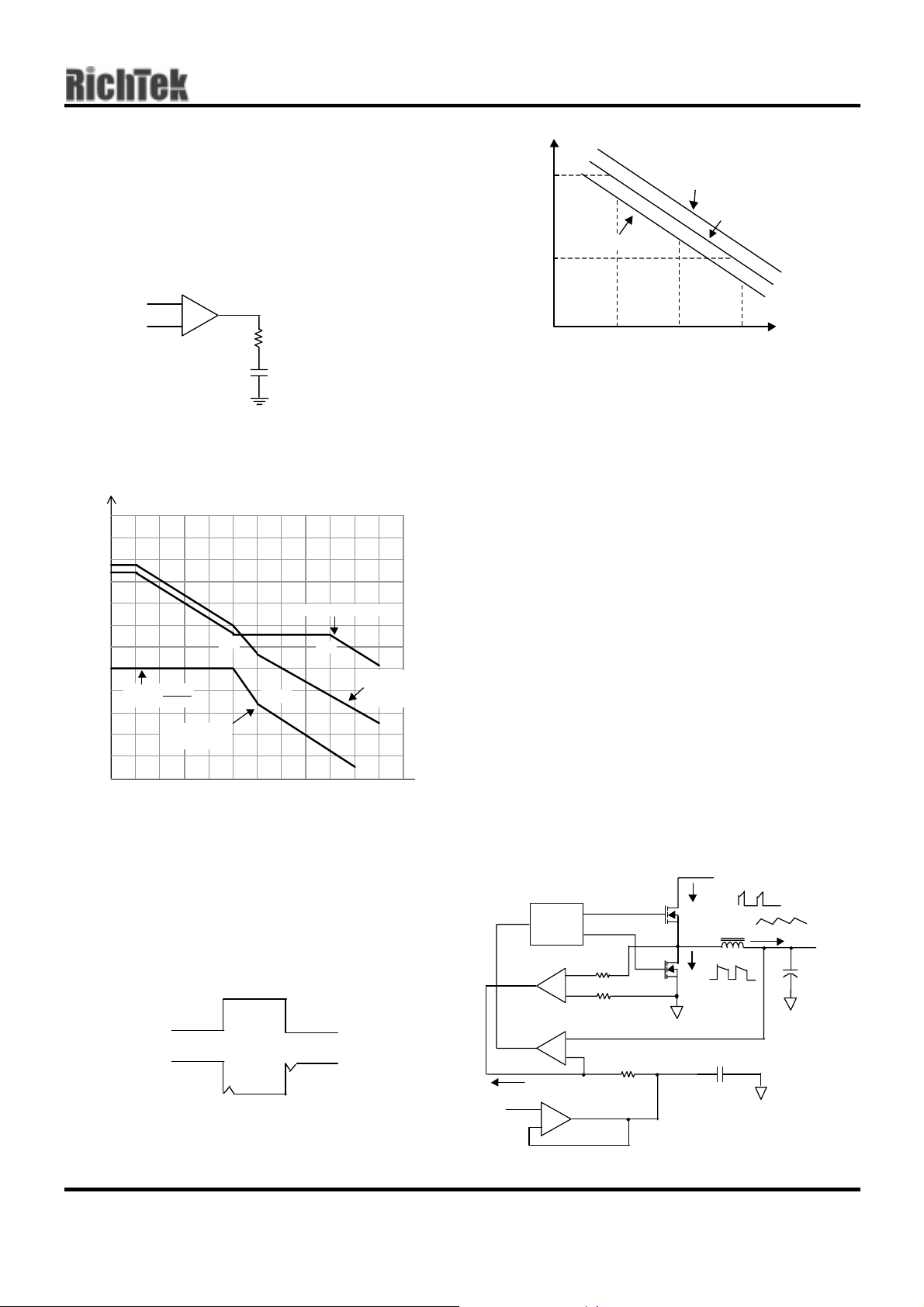
The PWM controller uses voltage-mode control for
output regulation. An internal pole-zero
compensation scheme is used with an active
capacitor and a passive resistor shown in Fig.8. The
zero FZ1 is fixed at about 1kHz to compensate the
output ‘s LC pole FLC. The compensation is to
16
Page 17
Preliminary RT9238
provide closed loop transfer function with 0 dB
crossing frequency and adequate phase margin. For
some suggestion LC combinations are L/C =
4µH/6000µF, 3uH/8000uF or 2µH/12000µF. Fig.9
shows an asymptotic plot of the DC-DC converter’s
gain vs. frequency.
+
EA
_
Active Cap
Fig.8 Error Amplifier Compensation
100
80
60
40
F
GAIN
Z1
F
LC
20
0
-20
-40
-60
V
IN
20log
V
P-P
MODULATOR
10 100 1K 10K 100K 1M
COMPENSATION
F
ESR
F
P1
CLOSED
LOOP
GAIN
Fig.9 PWM Bode Plot
Volt
V
CORE
Maxim um
V
CORE
Typical
CORE
V
1.70
1.60
V
CORE
Mini mum
10 20 30 A
Fig.11 V
CORE
Load Line
Two things have to be completed at load transient
response, first is to sense the instantaneous load
current, second is real time to drop the V
based on the loadlines
. A RT9238 internal trans-
CORE
voltage
conductance (Gm) amplifier sample the on-state drop
across the lower MOSFET per clock cycle, the
voltage drop is simply R
DS-ON X inductor current IL. In
step-down DC-DC converter, the IL is relative to load
current. The transferred rate of the Gm amplifier is
1/3k, this mean the current output of Gm amplifier is
I
SENSE = R
DS(ON)
x IL/3k.
Fig.12 shown the voltage droop tuning circuit, a
DACOUT buffer amplifier connect a RF resistor to the
non-inverting input of the PWM error amplifier, when
load transient happened, the feedback
ISENSE current
fitted to the non-inverting input of the PWM error
amplifier to drop the VCORE voltage. The drop
voltage is equal to
V
DROOP
= I
SENSE
x RF
Transient Response
Modern micro-processsor’s power supply request a
voltage droop at load transient response and a
loadlines at static state load changing as shown in
Fig.10, and Fig.11.
∆ I
O
V
Ripple
CORE
Fig.10 Transient Response
Control
Logic
Sample Hold
Gm
_
Low Side Current Sense
Error Amp
VNI
Isense
+
_
DAC Bu ffer
_
COMP
REF
UG
PHASE
RS
+
RS
+
LG
RF
REFOUT
Referen ce Output
IM1
IM2
Rds-on
V5V
IL
VCORE
+
Fig.12 Voltage Droop Tuning
DS9238-01 July 2001 www.richtek.com
17
Page 18
RT9238 Preliminary
CORE
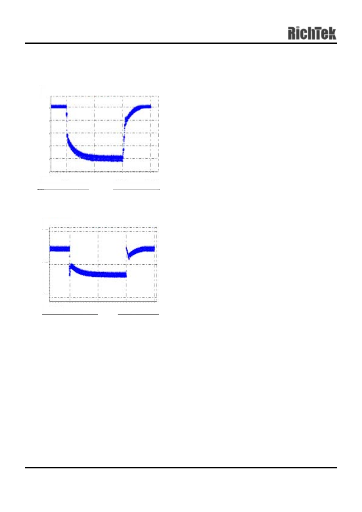
Fig.13, 14 shown the I
and VCORE wave
SENSE
forms.
0µA
-20µA
-40µA
SENSE
I
-60µA
-80µA
1.6ms 1.8ms 2.0ms
Time
Time
SENSE
Time
Current
Time
1.4V
1.3V
1.2V
Fig.14 V
Fig.13 I
1.6ms 1.8ms 2.0ms 2.2ms
Wave Form at Load Transient
CORE
Component Selection Guidelines
Output Capacitor Selection
The output capacitors for each output have unique
requirements. In general the output capacitors should
be selected to meet the dynamic regulation
requirements. Additionally, the PWM converter
requires an output capacitor to filter the current ripple.
The load transient for the microprocessor core
requires high quality capacitors to supply the high
slew rate (di/dt) current demands.
PWM Output Capacitors
Modern microprocessors produce transient load rates
above 1A/ns. High frequency capacitors initially
supply the transient current and slow the load rate-ofchange seen by the bulk capacitors. The bulk filter
capacitor values are generally determined by the
ESR (effective series resistance) and voltage rating
requirements rather than actual capacitance
requirements.
High frequency decoupling capacitors should be
placed as close to the power pins of the load as
physically possible. Be careful not to add inductance
in the circuit board wiring that could cancel the
usefulness of these low inductance components.
Consult with the manufacturer of the load on specific
decoupling requirements.
Use only specialized low-ESR capacitors intended for
switching-regulator applications for the bulk
capacitors. The bulk capacitor’s ESR determines the
output ripple voltage and the initial voltage drop
following a high slew-rate transient’s edge. An
aluminum electrolytic capacitor’s ESR value is related
to the case size with lower ESR available in larger
case sizes. However, the equivalent series
inductance (ESL) of these capacitors increases with
case size and can reduce the usefulness of the
capacitor to high slew-rate transient loading.
Unfortunately, ESL is not a specified parameter.
Work with your capacitor supplier and measure the
capacitor’s impedance with frequency to select a
suitable component. In most cases, multiple
electrolytic capacitors of small case size perform
better than a single large case capacitor.
Linear Output Capacitors
The output capacitors for the linear regulators provide
dynamic load current. Thus capacitors C
and C
should be selected for transient load
OUT4
OUT2
, C
OUT3
regulation.
PWM Output Inductor Selection
The PWM converter requires an output inductor. The
output inductor is selected to meet the output voltage
ripple requirements and sets the converter’s
,
www.richtek.com DS9238-01 July 2001
18
Page 19

Preliminary RT9238
response time to a load transient. The inductor value
determines the converter’s ripple current and the
ripple voltage is a function of the ripple current. The
ripple voltage and current are approximated by the
following equations:
V
OUT
V
IN
ESRIVOUT ×∆=∆
OUTIN
VV
−
I ×
=∆
S
LF
×
Increasing the value of inductance reduces the ripple
current and voltage. However, large inductance
values increase the converter’s response time to a
load transient.
One of the parameters limiting the converter’s
response to a load transient is the time required to
change the inductor current. Given a sufficiently fast
control loop design, the RT9238 will provide either
0% or 100% duty cycle in response to a load
transient. The response time is the time interval
required to slew the inductor current from an initial
current value to the post-transient current level.
During this interval the difference between the
inductor current and the transient current level must
be supplied by the output capacitor(s). Minimizing the
response time can minimize the output capacitance
required.
The response time to a transient is different for the
application of load and the removal of load. The
following equations give the approximate response
time interval for application and removal of a transient
load:
Input Capacitor Selection
The important parameters for the bulk input capacitor
are the voltage rating and the RMS current rating. For
reliable operation, select bulk input capacitors with
voltage and current ratings above the maximum input
voltage and largest RMS current required by the
circuit. The capacitor voltage rating should be at least
1.25 times greater than the maximum input voltage.
The maximum RMS current rating requirement for the
input capacitors of a buck regulator is approximately
1/2 of the DC output load current. Worst-case RMS
current draw in a circuit employing the RT9238
amounts to the largest RMS current draw of the
switching regulator.
Use a mix of input bypass capacitors to control the
voltage overshoot across the MOSFETs. Use
ceramic capacitance for the high frequency
decoupling and bulk capacitors to supply the RMS
current. Small ceramic capacitors can be placed very
close to the upper MOSFET to suppress the voltage
induced in the parasitic circuit impedances.
For a through-hole design, several electrolytic
capacitors (Panasonic HFQ series or Nichicon PL
series or Sanyo MV-GX or equivalent) may be
needed. For surface mount designs, solid tantalum
capacitors can be used, but caution must be
exercised with regard to the capacitor surge current
rating. These capacitors must be capable of handling
the surge current at power-up. The TPS series
available from AVX, and the 593D series from
Sprague are both surge current tested.
RISE
t
×
=
OUTIN
VV
−
FALL
t
=
TRANO
IL
×
OUT
V
MOSFET Selection/Considerations
The RT9238 requires 5 external transistors. Two N-
TRANO
IL
channel MOSFETs are employed by the PWM
where: I
is the response time to the application of load, and
t
is the response time to the removal of load. Be
FALL
sure to check both of these equations at the minimum
and maximum output levels for the worst case
response time.
DS9238-01 July 2001 www.richtek.com
is the transient load current step, t
TRAN
RISE
converter. The GTL, AGP, and memory linear
controllers can each drive a MOSFET or a NPN
bipolar as a pass transistor. All these transistors
should be selected based upon R
DS(ON)
, current
gain, saturation voltages, gate supply requirements,
and thermal management considerations.
19
Page 20
RT9238 Preliminary
−×=
PWM MOSFET Selection and Considerations
In high-current PWM applications, the MOSFET
power dissipation, package selection and heatsink
are the dominant design factors. The power
dissipation includes two main loss components:
conduction losses and switching losses. These
losses are distributed between the upper and lower
MOSFET according to the duty factor. The
conduction losses are the main component of power
dissipation for the lower MOSFETs. Only the upper
MOSFET has significant switching losses, since the
lower device turns on and off into near zero voltage.
The equations presented assume linear voltagecurrent transitions and do not model power losses
due to the lower MOSFET’s body diode or the output
capacitances associated with either MOSFET. The
gate charge losses are dissipated by the controller IC
(RT9238) and do not contribute to the MOSFETs’
heat rise. Ensure that both MOSFETs are within their
maximum junction temperature at high ambient
temperature by calculating the temperature rise
according to package thermal resistance
specifications. A separate heatsink may be necessary
depending upon MOSFET power, package type,
ambient temperature and air flow .
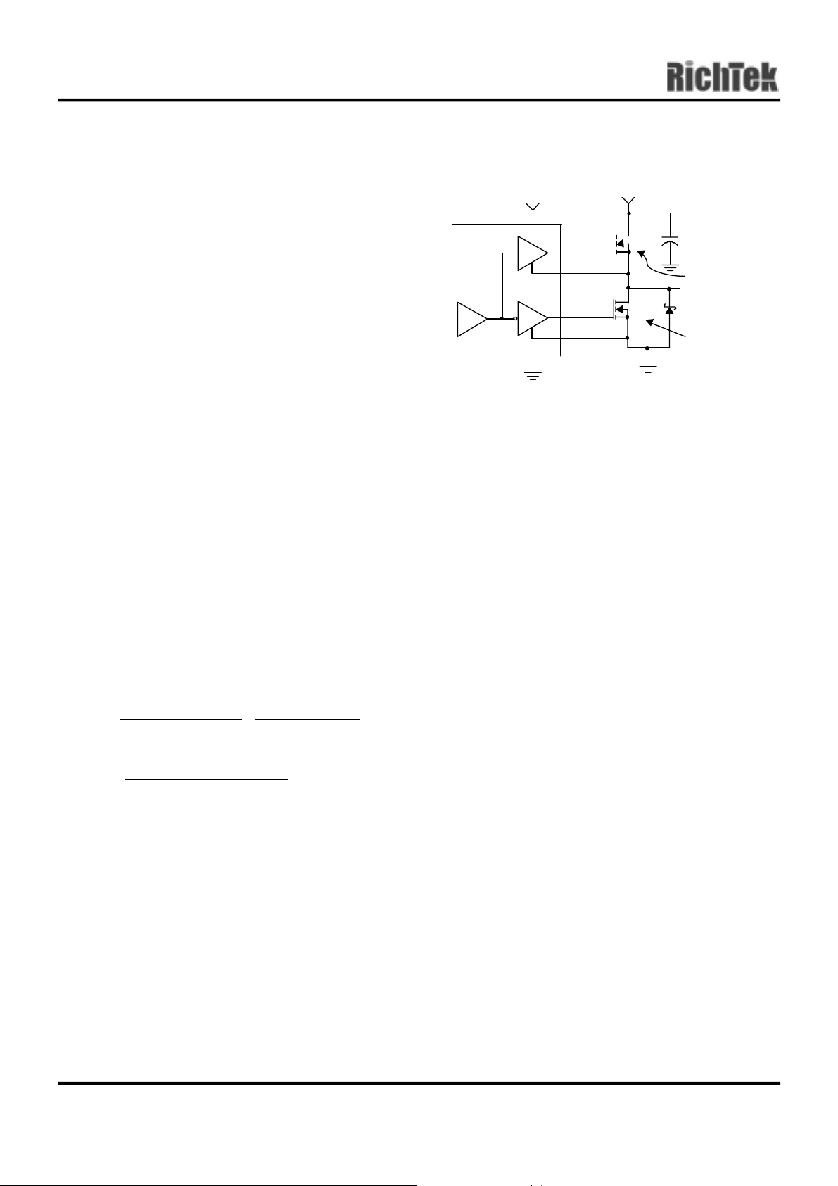
P
UPPER
LOWER
P
The R
2
O
=
2
O
=
is different for the two equations above
DS(ON)
VRI
××
OUT)ON(DS
IN
V
V
+
)VV(RI
−××
OUTIN)ON(DS
IN
FtVI
SSWINO
×××
2
even if the same device is used for both. This is
because the gate drive applied to the upper MOSFET
is different than the lower MOSFET. Fig.15 shows the
gate drive where the upper MOSFET’s gate-tosource voltage is approximately V
less the input
CC
supply. For +5V main power and +12VDC for the
bias, the approximate gate-to-source voltage of Q1 is
7V. The lower gate drive voltage is about 8V. A logiclevel MOSFET is a good choice for Q1 and a logiclevel MOSFET can be used for Q2 if its absolute
gate-to-source voltage rating exceeds the maximum
voltage applied to V
+12V
VCC
_
+
GND
Fig.15 Upper Gate Drive-direct V
.
CC
UGATE
PHASE
LGATE
PGND
+5V OR LE SS
Q1
Q2
CR1
NOTE:
V
GS
NOTE:
V
GS
CC
≈ V
≈ 8V
Drive
CC
- 5V
Rectifier CR1 is a clamp that catches the negative
inductor swing during the dead time between the turn
off of the lower MOSFET and the turn on of the upper
MOSFET. For best results, the diode must be a
surface-mount Schottky type to prevent the parasitic
MOSFET body diode from conducting. It is
acceptable to omit the diode and let the body diode of
the lower MOSFET clamp the negative inductor
swing, but one must ensure the PHASE node
negative voltage swing does not exceed -3V to -5V
peak. The diode’s rated reverse breakdown voltage
must be equal or greater to 1.5 times the maximum
input voltage.
Linear Controllers Transistor Selection
The RT9238 linear controllers are compatible with
both NPN bipolar as well as N-channel MOSFET
transistors. The main criteria for selection of pass
transistors for the linear regulators is package
selection for efficient removal of heat. The power
dissipated in a linear regulator is
)VV(IP OUTINOLINEAR
Select a package and heatsink that maintains the
junction temperature below the maximum desired
temperature with the maximum expected ambient
temperature.
When selecting bipolar NPN transistors for use with
the linear controllers, insure the current gain at the
www.richtek.com DS9238-01 July 2001
20
Page 21

Preliminary RT9238
given operating VCE is sufficiently large to provide the
desired output load current when the base is fed with
the minimum driver output current.
In order to ensure the strict timing/level requirement
of OUT4, a NPN transistor is recommended for use
as a pass element on this output (Q5). An low gate
threshold NMOS could be used, but meeting the
requirements would then depend on the VCC bias
being sufficiently high to allow control of the
MOSFET.
DS9238-01 July 2001 www.richtek.com
21
Page 22
RT9238 Preliminary
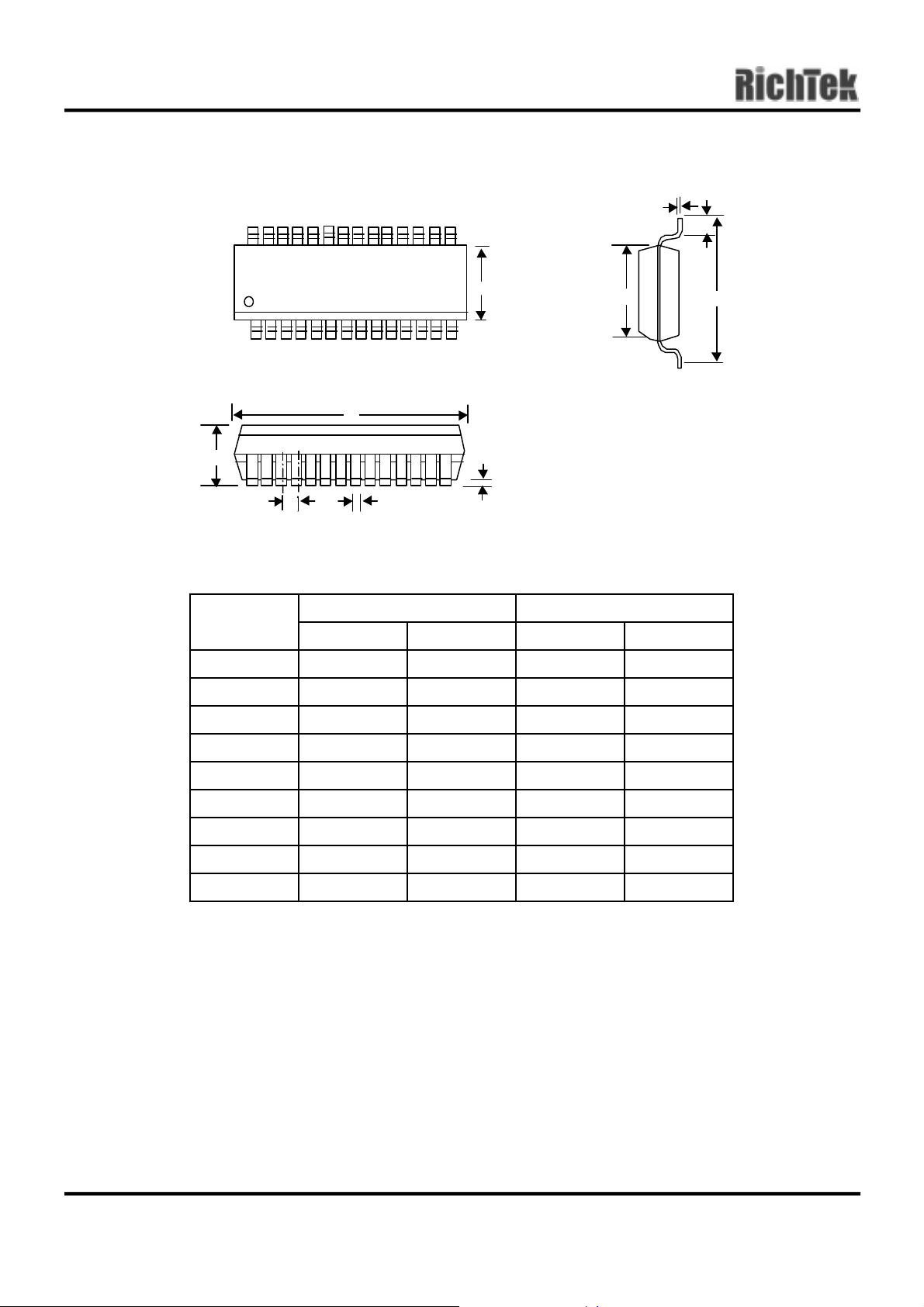
Package Information
H
M
B
A
C
FD
Dimensions In Millimeters Dimensions In Inches
Symbol
Min Max Min Max
A 17.704 18.110 0.697 0.713
B 7.391 7.595 0.291 0.299
C 2.362 2.642 0.093 0.104
I
B
J
D 0.330 0.508 0.013 0.020
F 1.194 1.346 0.047 0.053
H 0.229 0.330 0.009 0.013
I 0.102 0.305 0.004 0.012
J 10.008 10.643 0.394 0.419
M 0.381 1.270
0.015 0.050
www.richtek.com DS9238-01 July 2001
22
Page 23

RT9238 Preliminary
DS9238-01 July 2001 www.richtek.com
23
Page 24

RT9238 Preliminary
RICHTEK TECHNOLOGY CORP.
Headquarter
5F, No. 20, Taiyuen Street, Chupei City
Hsinchu, Taiwan, R.O.C.
Tel: (8863)5526789 Fax: (88 63)5526611
www.richtek.com DS9238-01 July 2001
RICHTEK TECHNOLOGY CORP.
Taipei Office (Marketing)
8F-1, No. 137, Lane 235, Paochiao Road, Hsintien City
Taipei County, Taiwan, R.O.C.
Tel: (8862)89191466 Fa x: (8862)89191465
Email: [email protected]
24
 Loading...