

Page 1

5V/12V Synchronous Buck PWM DC-DC Controller
RT9214
General Description
The RT9214 is a high efficiency synchronous buck PWM
controllers that generate logic-supply voltages in PC based
systems. These high performance , single output devices
include internal soft-start, frequency compensation
networks and integrates all of the control, output
adjustment, monitoring and protection functions into a
single package.
The device operating at fixed 300kHz frequency provides
an optimum compromise between efficiency, external
component size, and cost.
Adjustable over-current protection (OCP) monitors the
voltage drop across the R
of the lower MOSFET for
DS(ON)
synchronous buck PWM DC-DC controller. The over-
current function cycles the soft-start in 4-times hiccup
mode to provide fault protection, and in an always hiccup
mode for under-voltage protection.
Ordering Information
RT9214
Package Type
S : SOP-8
SP : SOP-8 (Exposed Pad-Option 1)
Operating Temperature Range
P : Pb Free with Commercial Standard
G : Green (Halogen Free with Commer cial Standard)
Note :
Richtek Pb-free and Green products are :
`RoHS compliant and compatible with the current require-
ments of IPC/JEDEC J-STD-020.
`Suitable for use in SnPb or Pb-free soldering processes.
`100% matte tin (Sn) plating.
Features
zz
Operating with 5V or 12V Supply Voltage
z
zz
zz
Drives All Low Cost N-Cha nnel MOSFETs
z
zz
zz
Voltage Mode PWM Control
z
zz
zz
300kHz Fixed Frequency Oscillator
z
zz
zz
Fast T r an sient Re sponse :
z
zz
`High-Speed GM Amplifier
`Full 0 to 100% Duty Ratio
zz
Internal Soft-Start
z
zz
zz
z Adaptive Non-Overlapping Gate Driver
zz
zz
z Over-Current Fault Monitor on MOSFET, No
zz
Current Sense Resistor Required
zz
z RoHS Compliant and 100% Lead (Pb)-Free
zz
Applications
z Graphic Card
z Motherboard, Desktop Servers
z IA Equipments
z Telecomm Equipments
z High Power DC-DC Regulators
Pin Configurations
(TOP VIEW)
BOOT
UGATE
GND
LGATE
BOOT
UGATE
GND
LGATE
2
3
4
2
3
4
SOP-8
NC
9
PHASE
8
OPS
7
FB
6
5
VCC
PHASE
8
OPS
7
FB
6
5
VCC
DS9214-13 September 2007
SOP-8 (Exposed Pad)
www.richtek.com
1
Page 2
RT9214
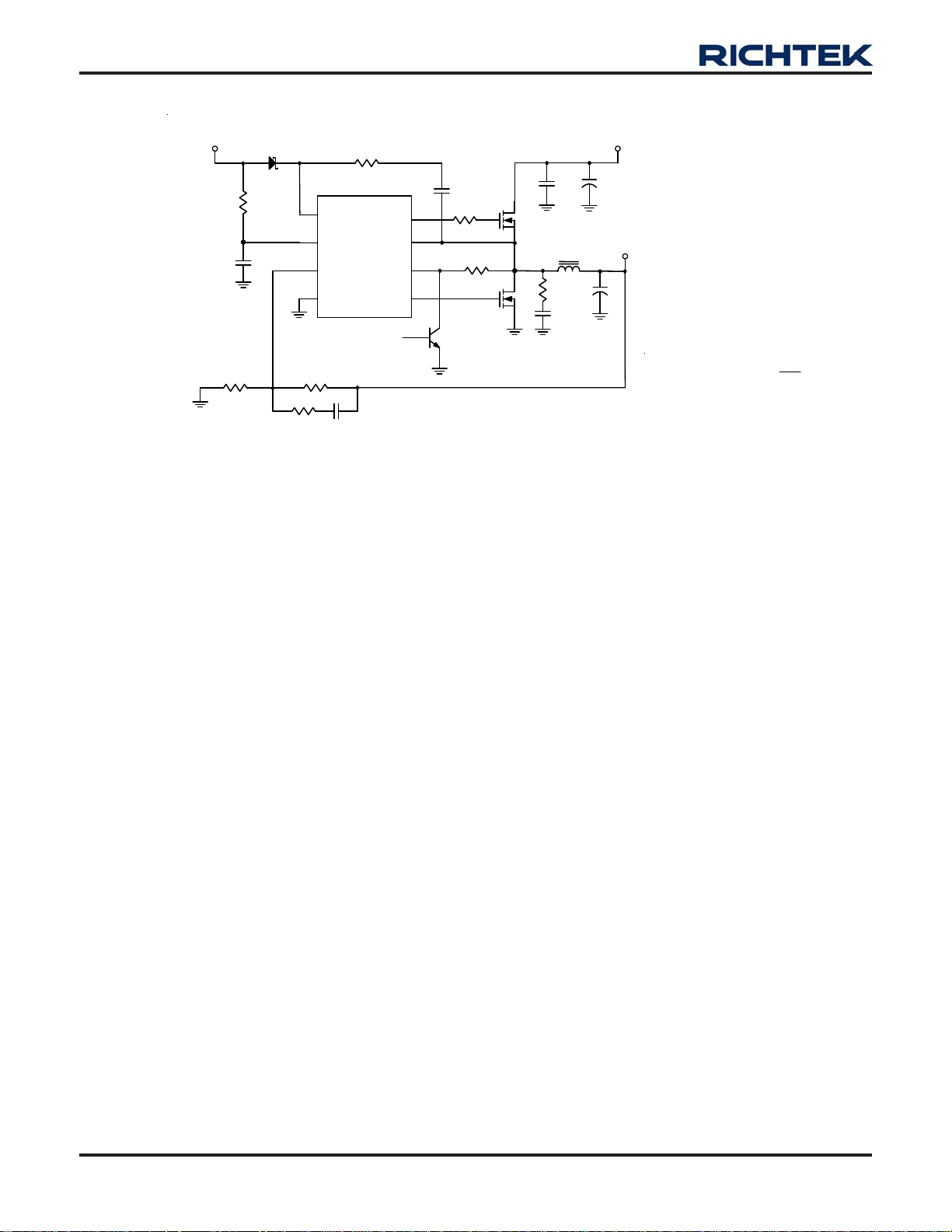
Typical Application Circuit
+
5
+
o
t
V
1
2
V
D1
1
4
N
1
4
8
R1
10
C1
1uF
R2
32
Functional Pin Description
1
5
6
3
R3
R4
200-1k
BOOT
VCC
FB
GND
68
RT9214
C5
0.1-0.33uF
R
B
O
2.2
Disable
T
O
UGATE
PHASE
OPS
LGATE
V
I
N
3
.
+
3
/
5
V
+
V
/
2
+
1
V
Q1
MU
Q2
ML
C3 C4
1uF
L1
3
u
H
R
C
C6 to C8
1000uFx3
470uF
V
O
U
T
R3
)
+×=
R2
voltage reference Internal:V
REF
(1VV
REFOUT
2%)(0.8V
±
C2
0.1uF
R
U
A
G
T
Q3
3904
E
2.2
ROCSET
2
8
7
4
>
BOOT (Pin 1)
Bootstrap supply pin for the upper gate driver. Connect
the bootstrap capacitor between BOOT pin and the PHASE
pin. The bootstrap capacitor provides the charge to turn
on the upper MOSFET.
UGA TE (Pin 2)
Upper gate driver output. Connect to the gate of high-
side power N-Channel MOSFET. This pin is monitored by
the adaptive shoot-through protection circuitry to
determine when the upper MOSFET has turned off.
GND (Pin 3)
Both signal and power ground for the IC. All voltage levels
are measured with respect to this pin. Ties the pin directly
to the low-side MOSFET source and ground plane with
the lowest impedance.
LGA TE (Pin 4)
Lower gate drive output. Connect to the gate of low-side
power N-Channel MOSFET. This pin is monitored by the
adaptive shoot-through protection circuitry to determine
when the lower MOSFET has turned off.
FB (Pin 6)
Switcher feedback voltage. This pin is the inverting input
of the error amplifier. FB senses the switcher output
through an external resistor divider network.
OPS (OCSET, POR and Shut-Down) (Pin 7)
This pin provides multi-function of the over-current setting,
UGATE turn-on POR sensing, and shut-down features.
Connecting a resistor (ROCSET) between OPS and
PHASE pins sets the over-current trip point.
Pulling the pin to ground resets the device and all external
MOSFETs are turned off allowing the output voltage power
rails to float.
This pin is also used to detect VIN in power on stage and
issues an internal POR signal.
PHASE (Pin 8)
Connect this pin to the source of the upper MOSFET and
the drain of the lower MOSFET.
NC [Exposed Pad (9)]
No Internal Connection.
VCC (Pin 5)
Connect this pin to a well-decoupled 5V or 12V bias
supply. It is also the positive supply for the lower gate
driver, LGATE.
www.richtek.com
2
DS9214-13 September 2007
Page 3
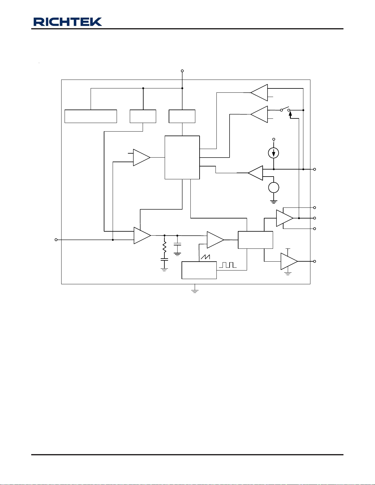
Function Block Diagram
RT9214
VCC
FB
Bias & Regulators
(3V_Logic & 3VDD_Analog)
0.6V
Reference
0.8VREF
+
-
+
GM
-
UV_S
EO
Power On
Reset
Soft-Start
&
Fault Logic
Oscillator
(300kHz)
EN
PH_M
+
-
0.1V
+
-
1.5V
3V
40uA
OPS
BOOT
UGATE
PHASE
LGATE
Gate
Control
Logic
-
0.4V
+
+
-
VCC
OC
+
-
DS9214-13 September 2007
GND
www.richtek.com
3
Page 4
RT9214
Absolute Maximum Ratings (Note 1)
z Supply Voltage, V
z BOOT, V
z PHASE to GND
BOOT
- V
-------------------------------------------------------------------------------------- 16V
CC
------------------------------------------------------------------------------------ 16V
PHASE
DC------------------------------------------------------------------------------------------------------------- −5V to 15V
< 200ns ------------------------------------------------------------------------------------------------------ −10V to 30V
z BOOT to PHASE ------------------------------------------------------------------------------------------ 15V
z BOOT to GND
DC------------------------------------------------------------------------------------------------------------- −0.3V to VCC+15V
< 200ns ------------------------------------------------------------------------------------------------------ −0.3V to 42V
z UGATE ------------------------------------------------------------------------------------------------------- V
z LGATE ------------------------------------------------------------------------------------------------------- GND - 0.3V to V
z Input, Output or I/O Voltage ----------------------------------------------------------------------------- GND-0.3V to 7V
z Power Dissipation, P
D
@ T
= 25°C (Note 4)
A
PHASE
- 0.3V to V
VCC
SOP-8 -------------------------------------------------------------------------------------------------------- 0.625W
SOP-8 (Exposed Pad) ----------------------------------------------------------------------------------- 1.33W
z Package Thermal Resistance
SOP-8, θJA-------------------------------------------------------------------------------------------------- 160°C/W
SOP-8 (Exposed Pad), θJA------------------------------------------------------------------------------ 75°C/W
z Junction Temperature ------------------------------------------------------------------------------------- 150°C
z Lead Temperature (Soldering, 10 sec.) --------------------------------------------------------------- 260°C
z Storage Temperature Range ---------------------------------------------------------------------------- −65°C to 150°C
z ESD Susceptibility (Note 2)
HBM (Human Body Mode) ------------------------------------------------------------------------------ 2kV
MM (Machine Mode) -------------------------------------------------------------------------------------- 200V
BOOT
+ 0.3V
+ 0.3V
Recommended Operating Conditions (Note 3)
z Supply Voltage, V
z Junction Temperature Range---------------------------------------------------------------------------- −40°C to 125°C
z Ambient Temperature Range ---------------------------------------------------------------------------- −40°C to 85°C
-------------------------------------------------------------------------------------- 5V ± 5%,12V ± 10%
CC
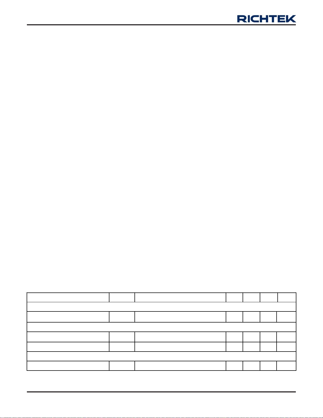
Electrical Characteristics
(V
= 5V/12V, T
CC
VCC Supply Current
Nominal Supply Current
Power-On Reset
POR Threshold
Hysteresis
Switcher Reference
Reference Voltage
= 25°C, unless otherwise specified)
A
Parameter Symbol Test Conditions Min Typ Max Units
I
CC
V
CCRTH
V
CCHYS
V
REF
UGATE and LGATE Open -- 6 15 mA
Rising
V
CC
0.35 0.5 -- V
= 12V
V
CC
-- 4.1 4.5 V
0.784 0.8 0.816 V
To be continued
www.richtek.com
4
DS9214-13 September 2007
Page 5
Oscillator
RT9214
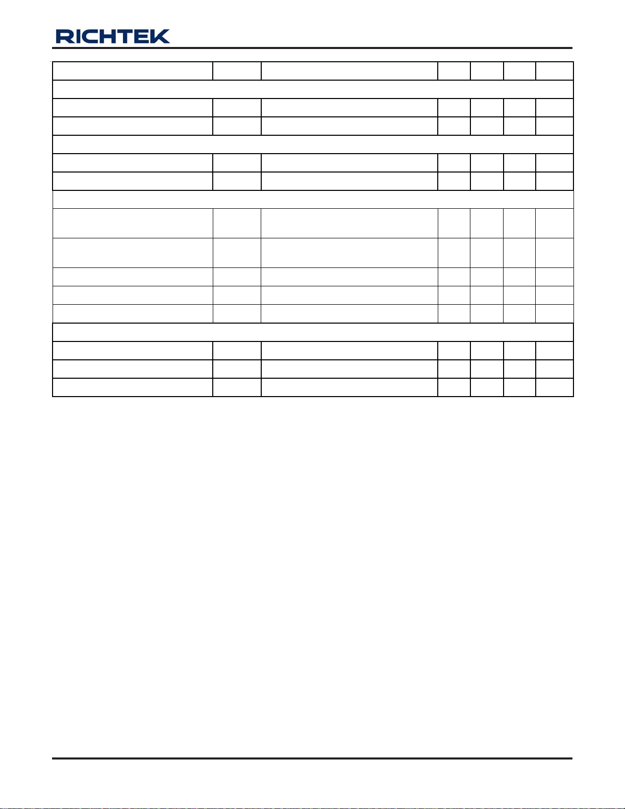
Parameter Symbol Test Conditions Min Typ Max Units
Free Running Frequency
Ramp Amplitude
f
OSC
ΔV
OSC
Error Amplifier (GM)
E/A Transconductance
Open Loop DC Gain
g
m
A
O
PWM Controller Gate Drivers (VCC = 12V)
Upper Gate Source
Upper Gate Sink
Lower Gate Source
Lower Gate Sink
Dead Time
Protection
FB Under-Voltage Trip
OC Current Source
Soft-Start Interval
I
UGATE
R
UGATE
I
LGATE
R
LGATE
T
DT
Δ
FBUVT
I
V
OC
T
SS
V
= 12V
CC
V
= 12V
CC
250 300 350 kHz
-- 1.5 --
V
P-P
-- 0.2 -- ms
-- 90 -- dB
− V
V
BOOT
V
V
V
UGATE
BOOT
UGATE
− V
− V
− V
VCC = 12V, V
VCC = 12V, V
-- -- 100
FB Falling 70 75 80
= 0V
PHASE
-- 3.5 --
PHASE
PHASE
PHASE
PHASE
LGATE
LGATE
= 12V,
= 6V
= 12V,
= 1V
= 6V
= 1V
0.6 1 --
-- 4 8
0.6 1 --
-- 3 5
35 40 45
A
Ω
A
Ω
ns
%
μA
ms
Note 1. Stresses listed as the above "Absolute Maximum Ratings" may cause permanent damage to the device. These are for
stress ratings. Functional operation of the device at these or any other conditions beyond those indicated in the
operational sections of the specifications is not implied. Exposure to absolute maximum rating conditions for extended
periods may remain possibility to affect device reliability.
Note 2. Devices are ESD sensitive. Handling precaution recommended.
Note 3. The device is not guaranteed to function outside its operating conditions.
Note 4. θ
is measured in the natural convection at TA = 25°C on a low effective thermal conductivity test board of
JA
JEDEC 51-3 thermal measurement standard.
DS9214-13 September 2007
www.richtek.com
5
Page 6
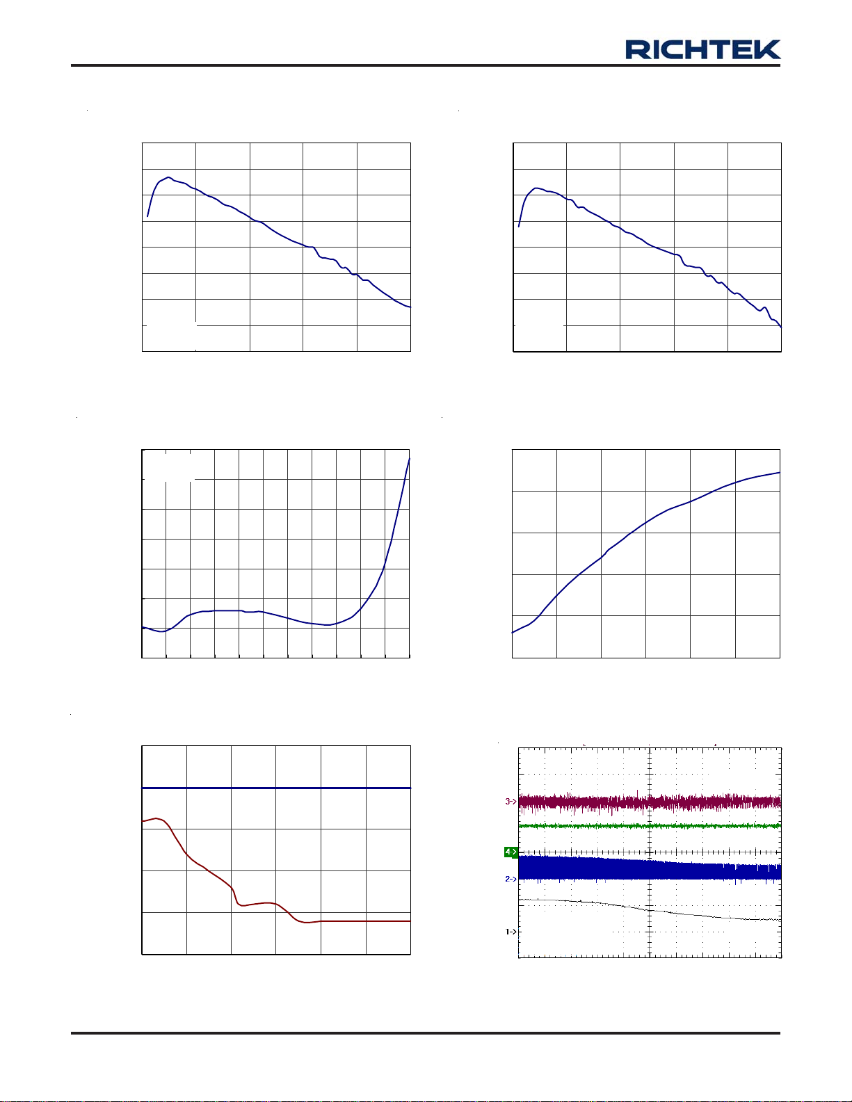
RT9214
)
Typical Operating Characteristics
(V
= 2.5V, unless otherwise specified )
OUT
1
Efficiency v s. Output Current
Efficiency vs. Output Current
1
Reference Voltage (V)
0.95
0.9
0.85
0.8
0.75
Efficiency(%)
0.7
0.65
V
= 12V
CC
V
= 5V
IN
0.6
0 5 10 15 20 25
Output Current (A)
Reference Voltage vs. Temperature
0.812
V
= 12V
CC
V
= 5V
IN
0.81
0.808
0.806
0.804
0.802
0.8
0.95
0.9
0.85
0.8
0.75
Efficiency(%)
0.7
0.65
V
= 5V
CC
V
= 5V
IN
0.6
0 5 10 15 20 25
Output Current (A)
Frequency vs. Temperature
350
330
310
290
Frequency (kHz
270
0.798
-40 -25 -10 5 20 35 50 65 80 95 110 125
Temperature
(°C)
POR vs. Temperature
4.75
4.5
4.25
4
3.75
POR Rising or Falling (V)
3.5
-40 -10 20 50 80 110 140
Rising
Falling
Temperature
(°C)
250
-40 -10 20 50 80 110 140
Temp erature
(°C)
VCC Switching
(100mV/Div)
V
OUT
I
OUT
UGATE
V
CC
VCC = 12Vto 5V
I
= 10A
OUT
V
= 5V
IN
Time (10ms/Div)
(10A/Div)
(20V/Div)
(10V/Div)
www.richtek.com
DS9214-13 September 2007
6
Page 7
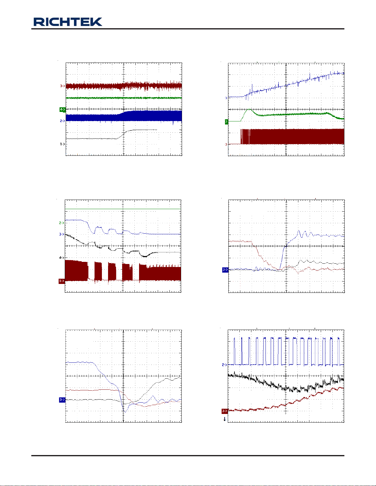
RT9214
V
OUT
I
OUT
UGATE
V
CC
V
CC
V
OUT
V
IN
VCC = 5V to 12V
I
= 10A, V
OUT
IN
VCC Switching
= 5V
Time (10ms/Div)
Power Off
(100mV/Div)
(10A/Div)
(20V/Div)
(10V/Div)
(10V/Div)
(2V/Div)
V
OUT
I
OUT
UGATE
VCC = V
I
= 25A
OUT
Power On
(500mV/Div)
(2A/Div)
(10V/Div)
Time (500us/Div)
Dead Time (Rising)
= 5V
IN
UGATE
UGATE
(5V/Div)
I
= 2A
OUT
VCC = 12V
V
= 5V
IN
I
= 25A
OUT
UGATE
PHASE
Time (5ms/Div)
Dead Time (Falling)
LGATE
Time (10ns/Div)
(2V/Div)
(10V/Div)
(5V/Div)
UGATE
(10V/Div)
V
OUT
(100mV/Div)
I
L
(10A/Div)
Time (25ns/Div)
Transient Response (Rising)
VCC = V
I
OUT
Freq. = 1/20ms, SR = 2.5A/us
= 12V
IN
= 0A to 15A
Time (5us/Div)
PHASE
LGATE
L = 2.2uH
C = 2000uF
DS9214-13 September 2007
www.richtek.com
7
Page 8
RT9214
UGATE
(10V/Div)
V
OUT
(100mV/Div)
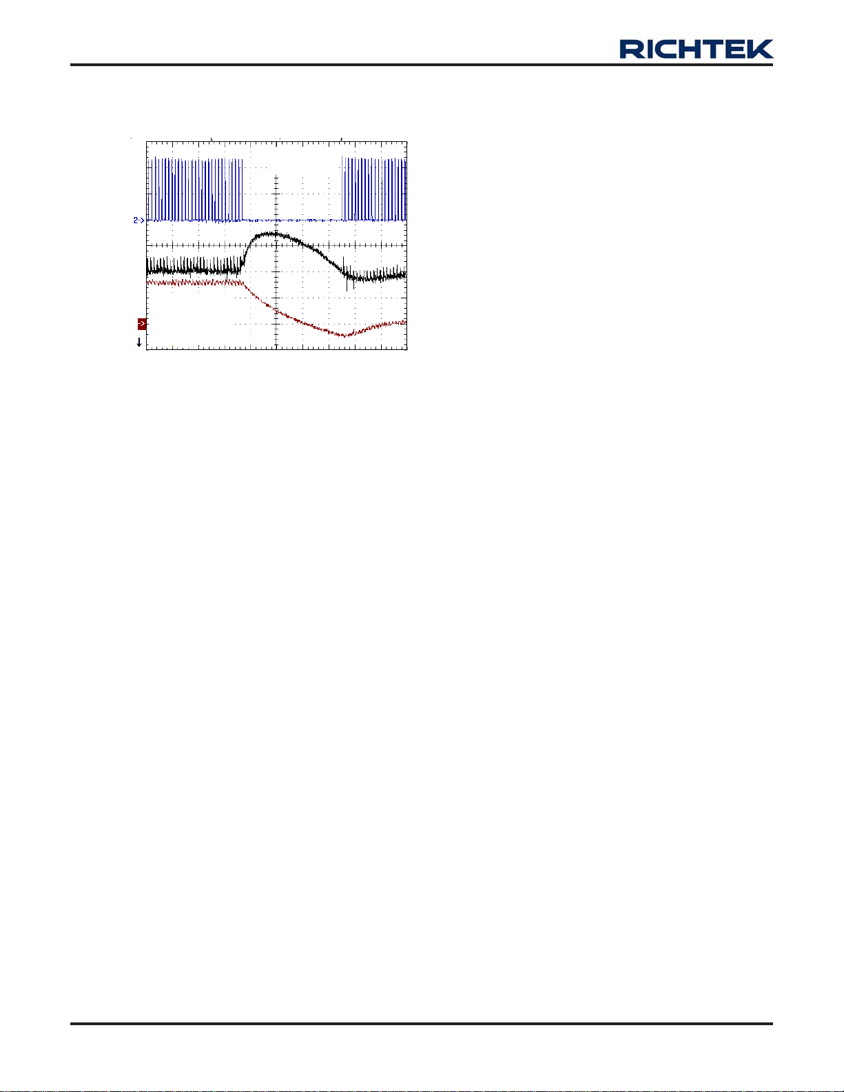
Transient Response (Falling)
L = 2.2uH
C = 2000uF
I
L
(10A/Div)
VCC = V
I
OUT
Freq. = 1/20ms
SR = 2.5A/us
= 12V
IN
= 15A to 0A
Time (25us/Div)
www.richtek.com
8
DS9214-13 September 2007
Page 9
Application Information
RT9214
Inductor Selection
The selection of output inductor is based on the
considerations of efficiency, output power and operating
frequency. Low inductance value has smaller size, but
results in low efficiency, large ripple current and high output
ripple voltage. Generally, an inductor that limits the ripple
current (ΔIL) between 20% and 50% of output current is
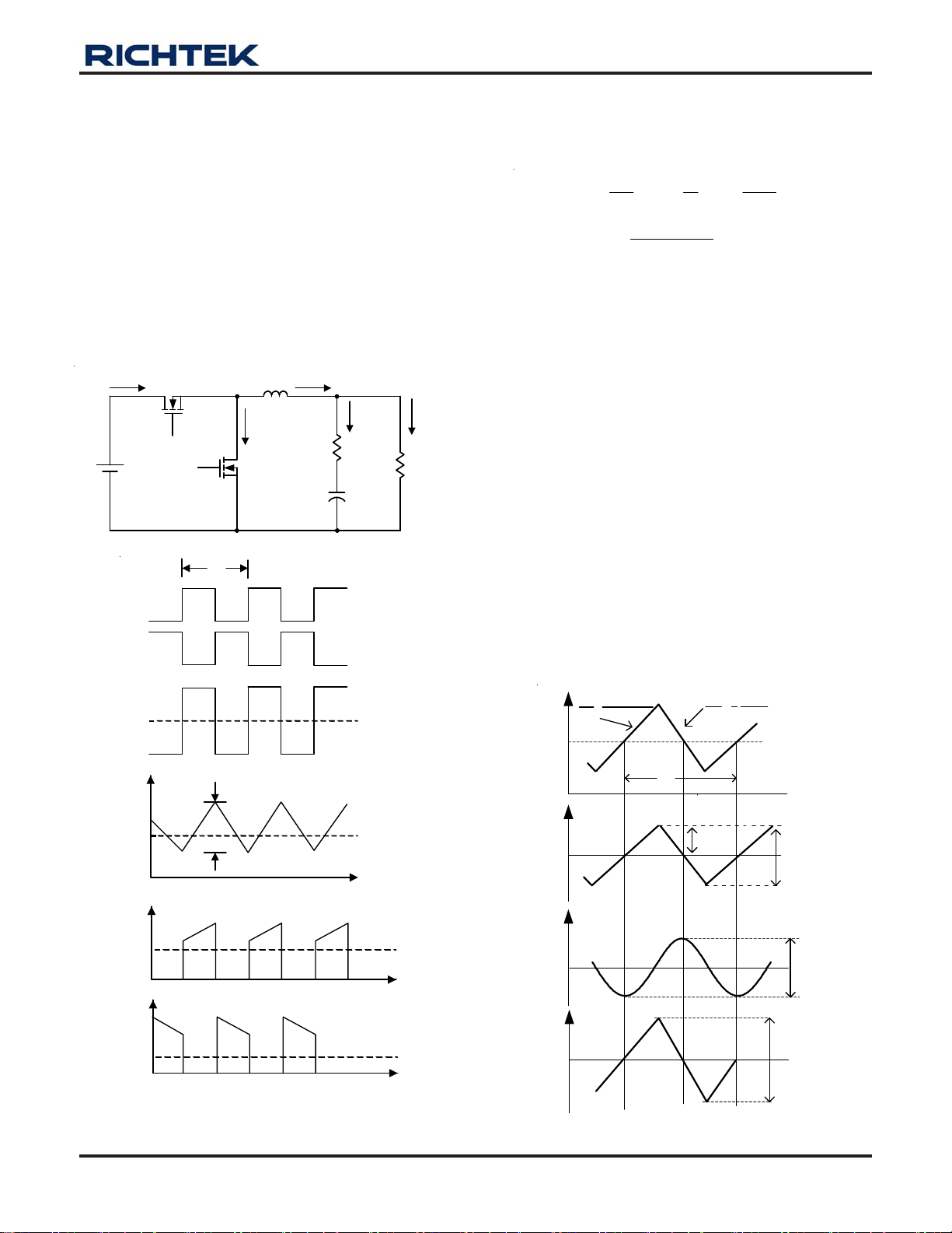
appropriate. Figure 1 shows the typical topology of
synchronous step-down converter and its related
waveforms.
i
S1
+
i
S1
V
IN
S2
V
TONT
g1
V
g2
S2
T
S
OFF
I
L
L
-
V
L
V
V
+
OC
+
OR
-
-
i
C
r
C
+
C
OUT
I
OUT
R
L
V
+
OUT
-
According to Figure 1 the ripple current of inductor can be
calculated as follows :
ΔI
VV L ; Δt; D
−= = =
IN OUT
L(V V )
=− ×
IN OUT
L
ΔtfsV
VfsΔI
D
V
OUT
××
IN L
V
OUT
IN
(1)
Where :
V
= Maximum input voltage
IN
V
= Output Voltage
OUT
Δt = S1 turn on time
ΔIL = Inductor current ripple
fS = Switching frequency
D = Duty Cycle
rC = Equivalent series resistor of output capacitor
Output Capa citor
The selection of output capacitor depends on the output
ripple voltage requirement. Practically, the output ripple
voltage is a function of both capacitance value and the
equivalent series resistance (ESR) rC. Figure 2 shows
the related waveforms of output capacitor.
VIN - V
OUT
V
L
- V
OUT
i
L
IL = I
ΔI
L
i
S1
i
S2
OUT
Figure 1. The waveforms of synchronous step-down
converter
di
VIN-V
L
=
L
t1 t2
OUT
i
L
dt
i
C
0
V
OC
V
OR
0
di
V
L
OUT
=
dt
L
I
OUT
T
S
ΔI
1/2
L
ΔI
L
ΔV
ΔIL x r
OC
c
Figure 2. The related waveforms of output capacitor
DS9214-13 September 2007
www.richtek.com
9
Page 10
RT9214
The AC impedance of output capacitor at operating
frequency is quite smaller than the load impedance, so
the ripple current (ΔI
) of the inductor current flows mainly
L
through output capacitor. The output ripple voltage is
described as :
ΔVΔVΔV
+=
OCOROUT
1
t2
rcΔIΔV
+×=
LOUT
C
O
rcΔIΔIΔV
LLOUT
dtic
∫
t1
1
OUT
CV8
OL
2
D)T(1
−+××=
S
(2)
(3)
(4)
where ΔVOR is caused by ESR and ΔVOC by capacitance.
For electrolytic capacitor application, typically 90 to 95%
of the output voltage ripple is contributed by the ESR of
output capacitor. So Equation (4) could be simplified as :
ΔV
= ΔIL x rc
OUT
(5)
Users could connect capacitors in parallel to get calculated
ESR.
Input Capacitor
The selection of input capacitor is mainly based on its
maximum ripple current capability. The buck converter
draws pulsewise current from the input capacitor during
the on time of S1 as shown in Figure 1. The RMS value of
ripple current flowing through the input capacitor is
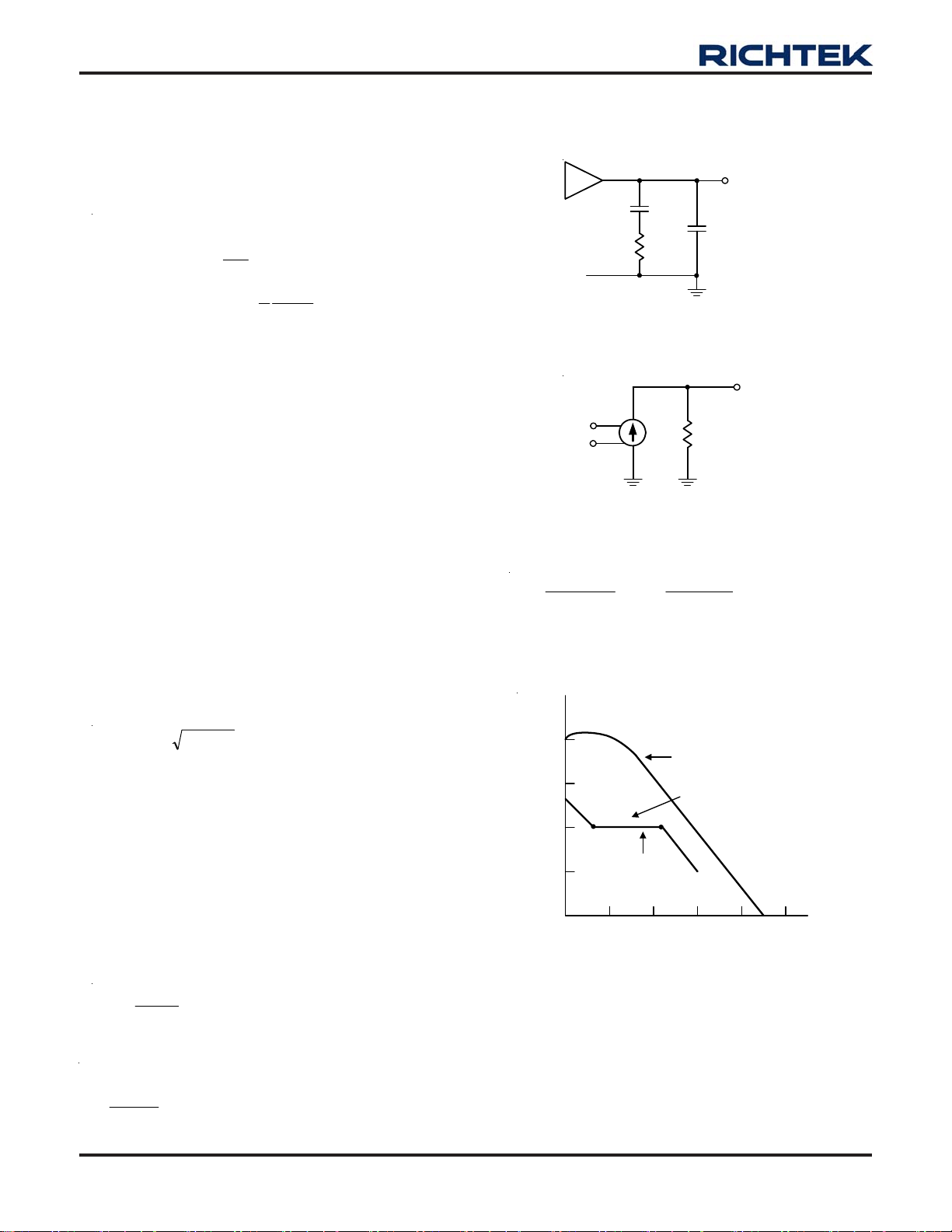
described as :
Z
is the shut impedance at the output node to ground
OUT
(see Figure 3 and Figure 4),
GM
C
1
R
1
V
OUT
C
2
Figure 3. A Type 2 error-amplifier with shut network to
ground
V
OUT
O
EA+
EA-
+
+
GM
-
R
Figure 4. Equivalent circuit
Pole and Zero :
F
P
1
=
×
F ;
Z
CR2
21
1
=
CR2
×
ππ
11
We can see the open loop gain and the Figure 3 whole
loop gain in Figure 5.
OUT
(A) D)D(1IIrms
−=
(6)
The input capacitor must be cable of handling this ripple
current. Sometime, for higher efficiency the low ESR
capacitor is necessarily.
PWM Loop Stability
RT9214 is a voltage mode buck converter using the high
gain error amplifier with transconductance (OTA,
Operational Transconductance Amplifier).
The transconductance :
dI
OUT
=
GM
dVm
The mid-frequency gain :
ZGMdVZdIdV
OUTINOUTOUTOUT
dV
dV
OUT
IN
==
G
www.richtek.com
10
GMZ
==
OUT
Open Loop, Unloaded Gain
A
Gain (dB)
F
Z
Gain = GMR
100 1000 10k 100k
Frequency (Hz)
Closed Loop, Unloaded Gain
F
P
1
B
Figure 5. Gain with the Figure 2 circuit
RT9214 internal compensation loop :
GM = 0.2ms, R1=75kΩ, C1 = 2.5nF, C2 = 10pF
DS9214-13 September 2007
Page 11
OPS (Over Current Setting, VIN_POR and Shutdown)
1.OCP
RT9214
Sense the low-side MOSFET’ s R
Connecting a resistor (R
sets the over-current trip point. R
) from this pin to the source of the upper MOSFET and the drain of the lower MOSFET
OCSET
OCSET
set the converter over-current trip point (I
to set over-current trip point.
DS(ON)
, an internal 40μA current source, and the lower MOSFET on resistance, R
) according to the following equation :
OCSET
I
OCSET
=
R
DS(ON)
OCSET
0.4VR40uA
−×
MOSFET lower the of
DS(ON)
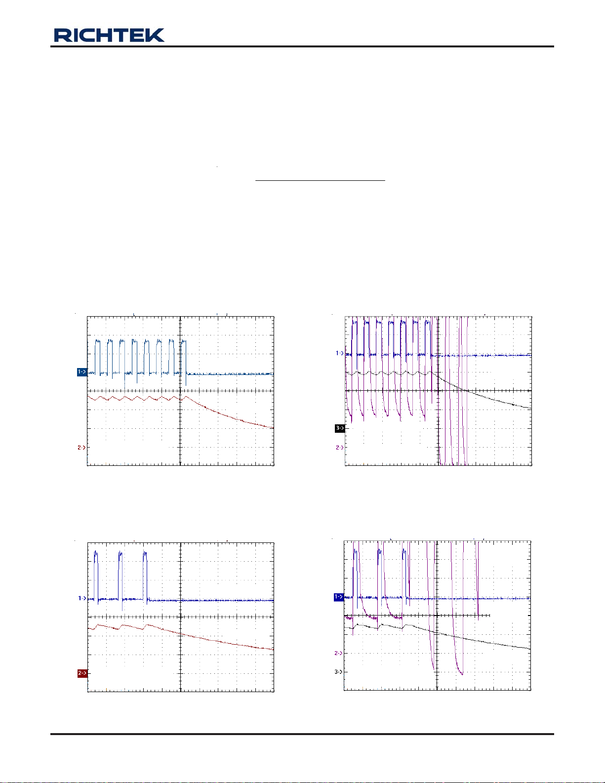
OPS pin function is similar to RC charging or discharging circuit, so the over-current trip point is very sensitive to
parasitic capacitance (ex. shut-down MOSFET) and the duty ratio.
Below Figures say those effect. And test conditions are Rocset = 15kΩ (over -current trip point = 20.6A), Low-side
MOSFET is IR3707.
OCP
UGATE (10V/Div)
OCP
UGATE
(10V/Div)
,
V
= 5V, VCC = 12V
IN
V
= 1.5V
OUT
V
= 12V, VCC = 12V
IN
V
= 1.5V
OUT
Time (5μs/Div)
OCP
Time (2.5μs/Div)
IL (10A/Div)
UGATE (10V/Div)
IL (10A/Div)
OPS (200mV/Div)
V
= 5V, VCC = 12V
IN
V
= 1.5V
OUT
V
= 12V, VCC = 12V
IN
V
= 1.5V
OUT
IL (10A/Div)
Time (5μs/Div)
OCP
OPS
(200mV/Div)
UGATE
(10V/Div)
IL (10A/Div)
Time (2.5μs/Div)
DS9214-13 September 2007
www.richtek.com
11
Page 12
RT9214
2. VIN_POR
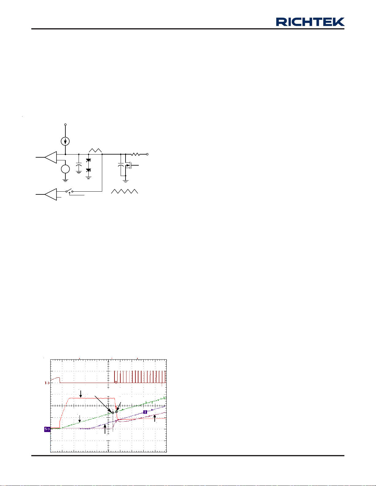
UGATE will continuously generate a 10kHz clock with
1% duty cycle before VIN is ready. VIN is recognized ready
by detecting V
falling). R
R
OCSET
OCSET
will keep V
crossing 1.5V four times (rising &
OPS
must be kept lower than 37.5kΩ for large
always higher than 1.5V. Figure 6
OPS
shows the detail actions of OCP and POR. It is highly
recommend-ed that R
3V
OC
POR_H
V
IN
PHASE_M
-
0.4V
+
10pF
+
-
+
-
1.5V
40uA
UGATE
be lower than 30kΩ.
OCSET
R
OPS
Cparasitic
1st 2nd 3rd 4th
(1) Internal Counter will count (V
four times (rising & falling) to recognize
V
IN
(2) R
OCSET
detect V
OCSET
Q2
DISABLE
OPS
waveform
is ready.
can be set too large. Or can
is ready (counter = 1, not equal 4)
IN
PHASE
OPS
Figure 6. OCP and VIN_POR actions
3. Shutdown
Pulling low the OPS pin by a small single transistor can
shutdown the RT9214 PWM controller as shown in typical
application circuit.
Soft Start
A built-in soft-start is used to prevent surge current from
power supply input during power on. The soft-start voltage
is controlled by an internal digital counter. It clamps the
ramping of reference voltage at the input of error amplifier
and the pulse-width of the output driver slowly. The typical
soft-start duration is 3ms.
> 1.5V)
1) Mode 1 (SS< Vramp_valley)
Initially the COMP stays in the positive saturation. When
SS< V
RAMP_Valley
, there is no non-inverting input available
to produce duty width. So there is no PWM signal and
V
is zero.
OUT
2) Mode 2 (V
When SS>V
RAMP_Valley
RAMP_Valley
< SS< Cross-over)
, SS takes over the non-inverting
input and produce the PWM signal and the increasing
duty width according to its magnitude above the ramp
signal. The output follows the ramp signal, SS. However
while V
increases, the difference between V
OUT
OUT
and
SSE (SS − VGS) is reduced and COMP leaves the
saturation and declines. The takeover of SS lasts until it
meets the COMP. During this interval, since the feedback
path is broken, the converter is operated in the open loop.
3) Mode3 ( Cross-over< SS < VGS + V
REF
)
When the Comp takes over the non-inverting input for PWM
Amplifier and when SSE (SS − VGS) < V
, the output of
REF
the converter follows the ramp input, SSE (SS − VGS).
Before the crossover, the output follows SS signal. And
when Comp takes over SS, the output is expected to follow
SSE (SS − VGS). Therefore the deviation of VGS is
represented as the falling of V
for a short while. The
OUT
COMP is observed to keep its decline when it passes the
cross-over, which shortens the duty width and hence the
falling of V
happens.
OUT
Since there is a feedback loop for the error amplifier, the
output’ s response to the ramp input, SSE (SS − V
GS
) is
lower than that in Mode 2.
4) Mode 4 (SS > VGS + V
When SS > VGS + V
the desired V
REF
signal and the soft start is completed
REF
)
REF
, the output of the converter follows
now.
SS_Internal
www.richtek.com
12
COMP
V
RAMP_Valley
SSE_Internal
Cross-over
VCORE
DS9214-13 September 2007
Page 13
RT9214
Under Voltage Protection
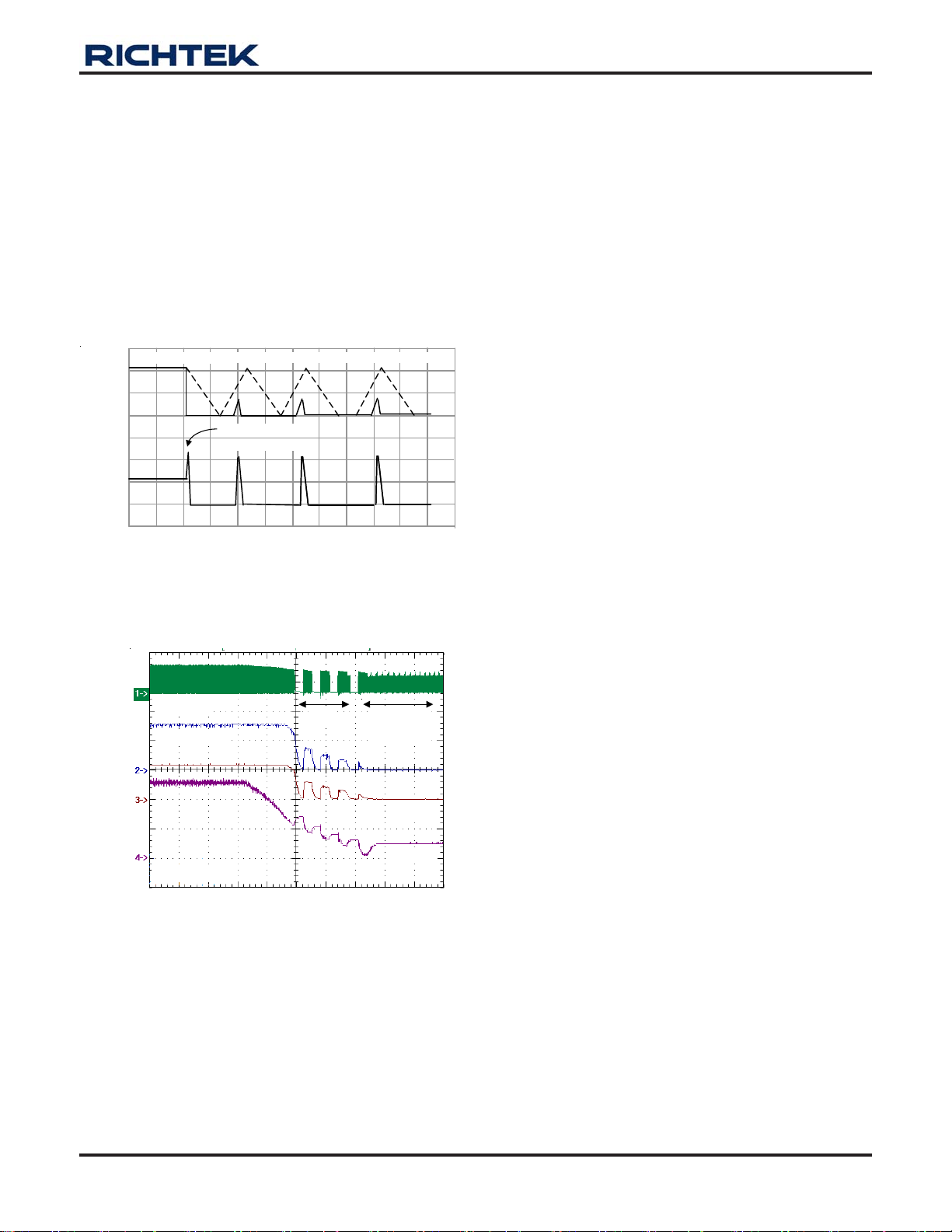
The voltage at FB pin is monitored and protected against
UV (under voltage). The UV threshold is the FB or FBL
under 80%. UV detection has 15μs triggered delay. When
OC is trigged, a hiccup restart sequence will be initialized,
as shown in Figure 7 Only 4 times of trigger are allowed
to latch off. Hiccup is disabled during soft-start interval,
but UV_FB has some difference from OC, it will always
trigger VIN power sensing after 4 times hiccup, as shown
in Figure 8.
Internal
COUNT = 1 COUNT = 2
4V
SS
2V
0V
0A
Inductor Current
OVERLOAD
APPLIED
T0
T1 T2 T3
COUNT = 3 COUNT = 4
T4
TIME
Figure 7. UV and OC trigger hiccup mode
Power Off
placement layout and printed circuit design can minimize
the voltage spikes induced in the converter. Consider, as
an example, the turn-off transition of the upper MOSFET
prior to turn-off, the upper MOSFET was carrying the full
load current. During turn-off, current stops flowing in the
upper MOSFET and is picked up by the low side MOSFET
or schottky diode. Any inductance in the switched current
path generates a large voltage spike during the switching
interval. Careful component selections, layout of the
critical components, and use shorter and wider PCB traces
help in minimizing the magnitude of voltage spikes.
There are two sets of critical components in a DC-DC
converter using the RT9214. The switching power
components are most critical because they switch large
amounts of energy, and as such, they tend to generate
equally large amounts of noise. The critical small signal
components are those connected to sensitive nodes or
those supplying critical bypass current.
The power components and the PWM controller should
be placed firstly. Place the input capacitors, especially
the high-frequency ceramic decoupling capacitors, close
to the power switches. Place the output inductor and
output capacitors between the MOSFETs and the load.
Also locate the PWM controller near by MOSFETs.
UGATE
V
FB
OUT
V
IN
(20V/Div)
(500mV/Div)
I
= 2A
OUT
UV
Time (10ms/Div)
V
Power
IN
Sensing
(2V/Div)
(2V/Div)
Figure 8, UV_FB trigger VIN power sensing
PWM Layout Considerations
MOSFETs switch very fast and efficiently. The speed with
which the current transitions from one device to another
causes voltage spikes across the interconnecting
impedances and parasitic circuit elements. The voltage
spikes can degrade efficiency and radiate noise, that results
in over-voltage stress on devices. Careful component
A multi-layer printed circuit board is recommended.
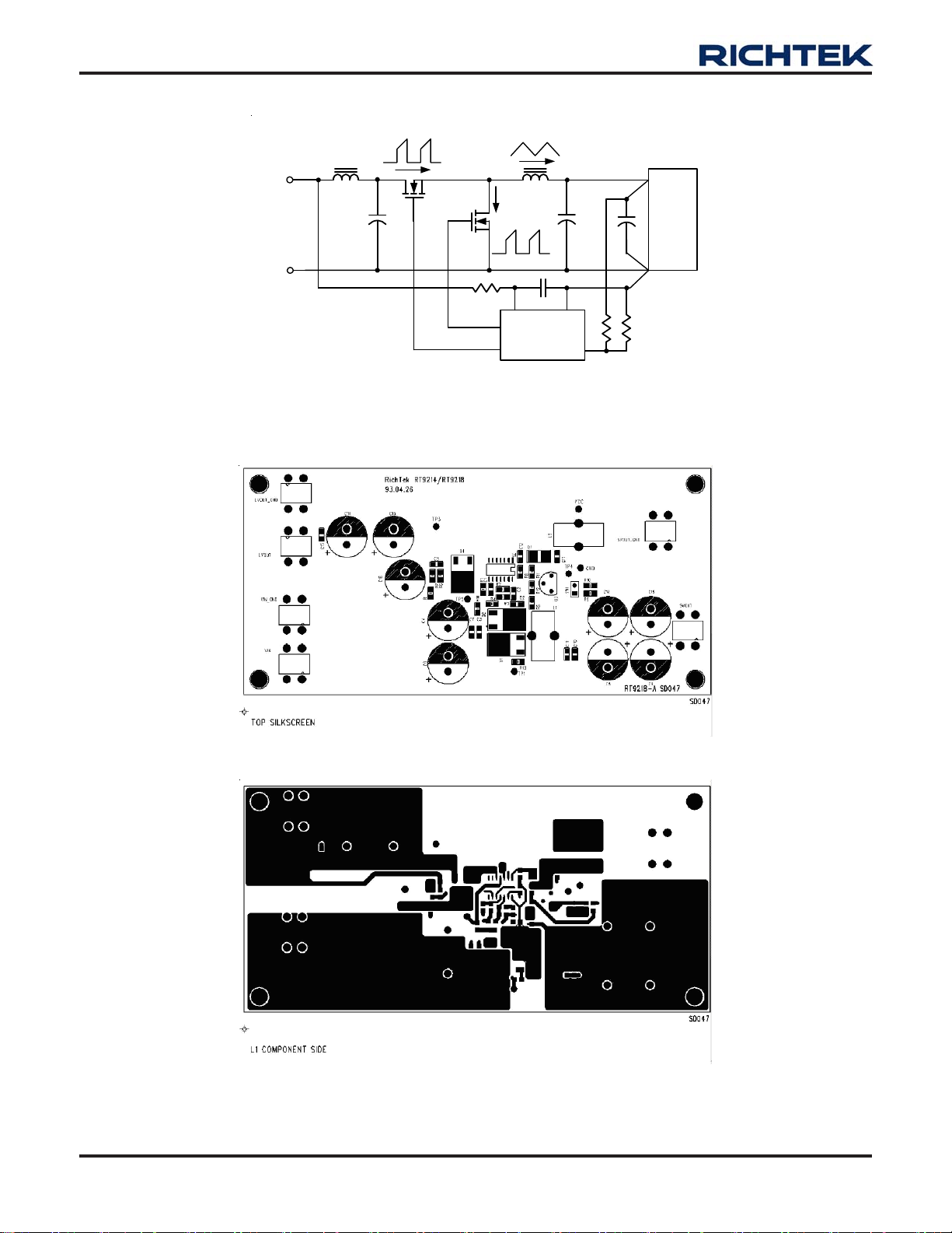
Figure 9 shows the connections of the critical components
in the converter. Note that the capacitors CIN and C
OUT
each of them represents numerous physical capacitors.
Use a dedicated grounding plane and use vias to ground
all critical components to this layer. Apply another solid
layer as a power plane and cut this plane into smaller
islands of common voltage levels. The power plane should
support the input power and output power nodes. Use
copper filled polygons on the top and bottom circuit layers
for the PHASE node, but it is not necessary to oversize
this particular island. Since the PHASE node is subjected
to very high dV/dt voltages, the stray capacitance formed
between these island and the surrounding circuitry will
tend to couple switching noise. Use the remaining printed
circuit layers for small signal routing. The PCB traces
between the PWM controller and the gate of MOSFET
and also the traces connecting source of MOSFETs should
be sized to carry 2A peak currents.
DS9214-13 September 2007
www.richtek.com
13
Page 14
RT9214
IQ1
5V/12V
+
GND
Q1
Q2
LGATE
UGATE
Figure 9. The connections of the critical components in the converter
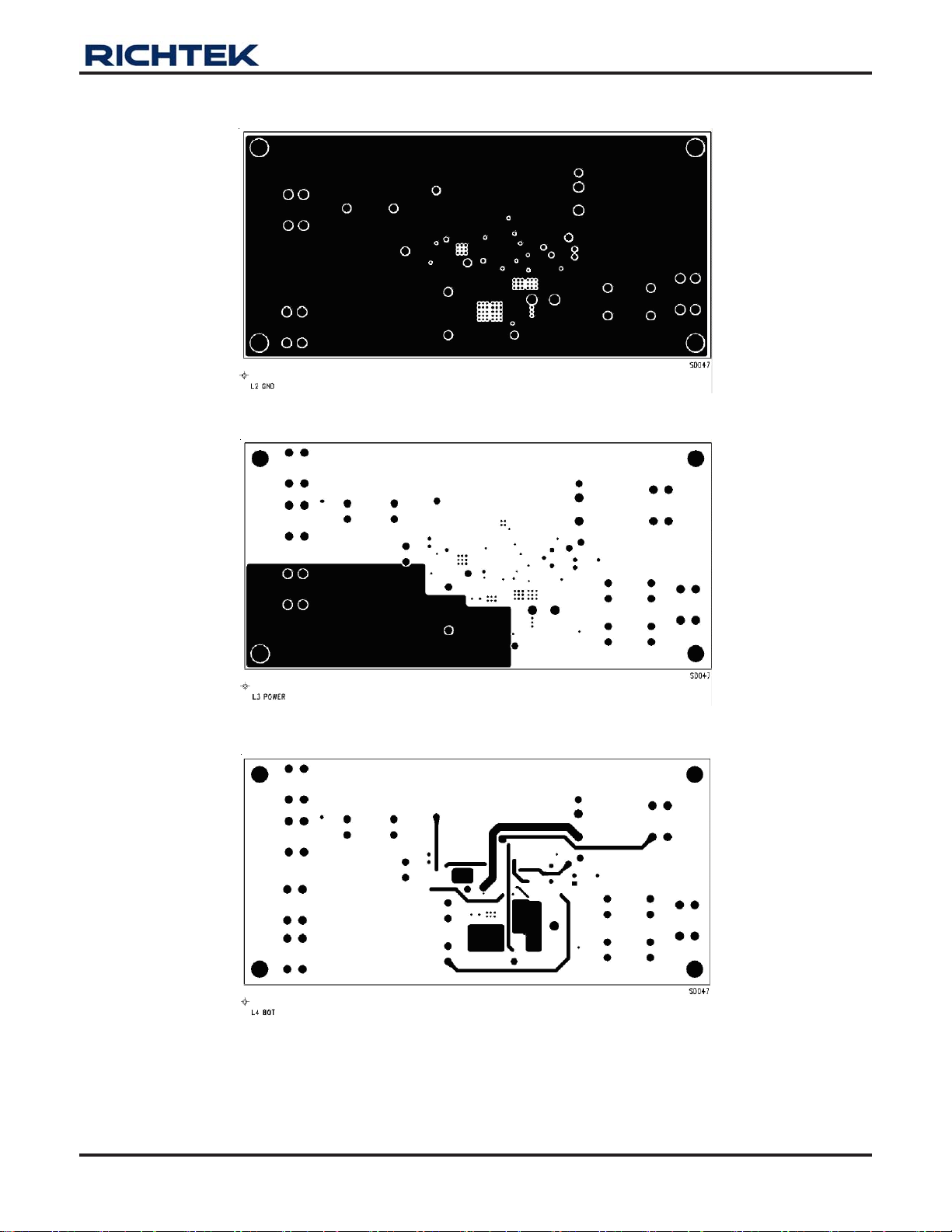
Below PCB gerber files are our test board for your reference :
IQ2
VCC
IL
GND
RT9214
+
FB
V
OUT
+
LOAD
www.richtek.com
14
DS9214-13 September 2007
Page 15
RT9214
According to our test experience, you must still notice two items to avoid noise coupling :
1.The ground plane should not be separated.
2.VCC rail adding the LC filter is recommended.
DS9214-13 September 2007
www.richtek.com
15
Page 16
RT9214
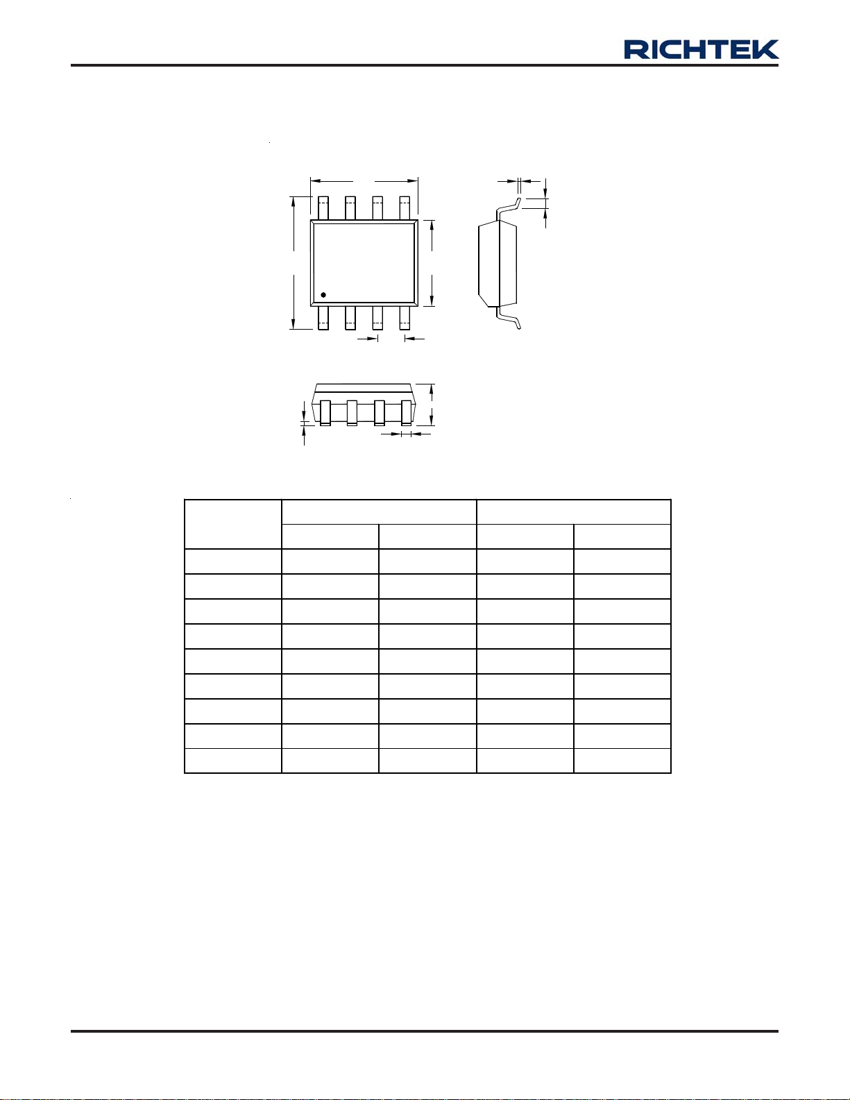
Outline Dimension
A
J
I
Dimensions In M illimeters Dimensions In Inches
Symbol
Min Max Min Max
A 4.801 5.004 0.189 0.197
B
F
C
D
H
M
B 3.810 3.988 0.150 0.157
C 1.346 1.753 0.053 0.069
D 0.330 0.508 0.013 0.020
F 1.194 1.346 0.047 0.053
H 0.170 0.254 0.007 0.010
I 0.050 0.254 0.002 0.010
J 5.791 6.200 0.228 0.244
M 0.400 1.270 0.016 0.050
8-Lead SOP Plastic Package
www.richtek.com
16
DS9214-13 September 2007
Page 17
RT9214
H
M
EXPOSED THERMAL PAD
(Bottom of Package)
A
Y
J
I
B
X
F
C
D
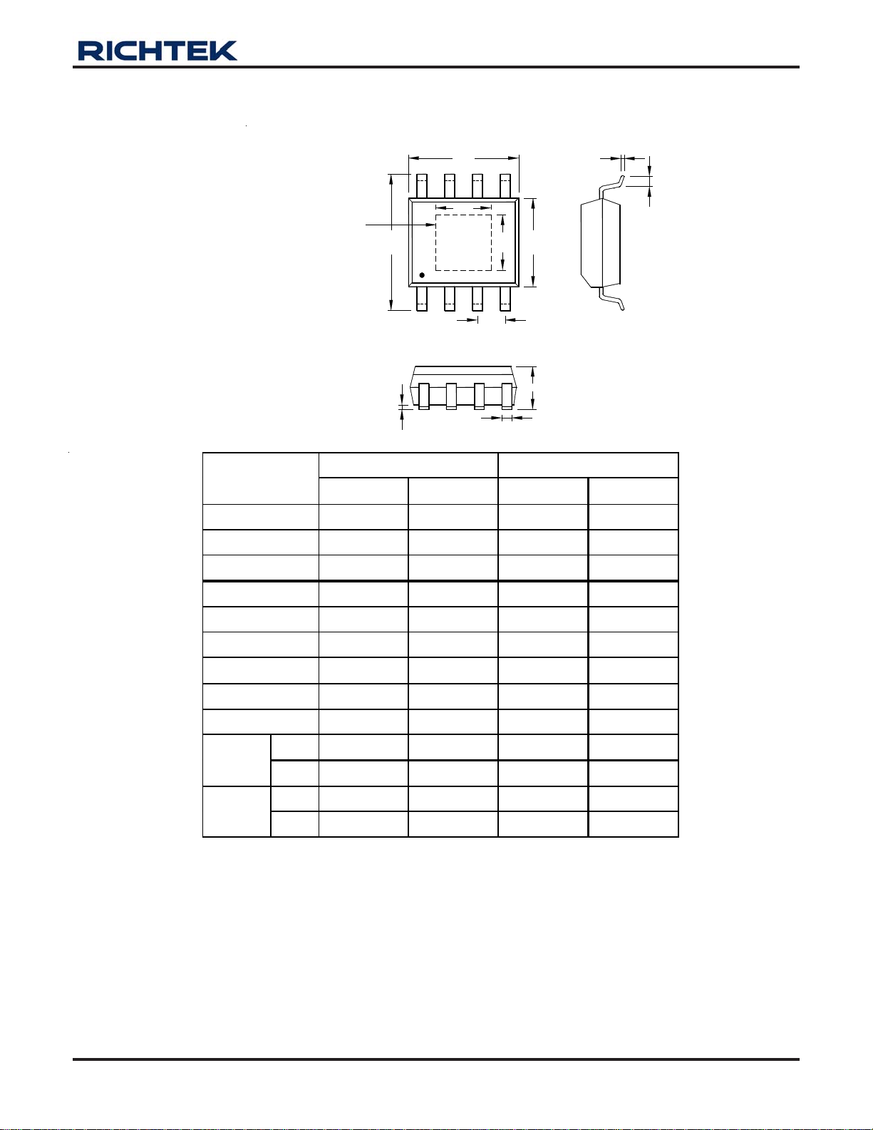
Dimensions In Millimeters Dimensions In Inches
Symbol
Min Max Min Max
A 4.801 5.004 0. 189 0.197
B 3.810 4.000 0. 150 0.157
C 1.346 1.753 0.053 0.069
D 0.330 0.510 0.013 0.020
F 1.19 4 1.34 6 0. 047 0.053
H 0.170 0.254 0.007 0.010
I 0.000 0.152 0. 000 0.006
J 5.79 1 6.200 0.228 0.244
M 0.406 1.270 0.016 0.050
X 2.000 2.30 0 0.079 0.091
Option 1
Y 2.000 2.30 0 0.079 0.091
X 2.100 2.50 0 0.083 0.098
Option 2
Y 3.000 3.50 0 0.118 0 .138
8-Lead SOP (Exposed Pad) Plastic Package
Richtek Technology Corporation
Headquarter
5F, No. 20, Taiyuen Street, Chupei City
Hsinchu, Taiwan, R.O.C.
Tel: (8863)5526789 Fax: (8863)5526611
Richtek Technology Corporation
Taipei Office (Marketing)
8F, No. 137, Lane 235, Paochiao Road, Hsintien City
Taipei County, Taiwan, R.O.C.
Tel: (8862)89191466 Fax: (8862)89191465
Email: [email protected]
DS9214-13 September 2007
www.richtek.com
17
 Loading...