

Page 1
RT8855
4/3/2/1-Phase PWM Controller for AMD AM2/AM2+ CPUs
General Description
The RT8855 is a 4/3/2/1-phase synchronous buck
controller with two integrated MOSFET drivers for CPU
power application a nd a single-pha se buck with integrated
MOSFET driver for North-Bridge (NB) chipset.The RT8855
uses differential inductor DCR current sense to achieve
phase current bala nce and a ctive voltage positioning. Other
features include adjustable operating frequency, power
good indication, external error-a mp compen sation, over
voltage protection, over current protection and enable/
shutdown for various a pplications. The RT8855 comes to
a small footprint with WQFN-48L 7x7 package.
Applications
z Desktop CPU Core Power
z Low V oltage, High Current DC/ DC Converter
Ordering Information
RT8855
Package Type
QW : WQFN -4 8 L 7 x 7 (W-Type )
Operating Temperature Range
G : Green (Halogen Free with Commer cial Sta n d ard)
Note :
Richtek Green products are :
` RoHS compliant and compatible with the current require-
ments of IPC/JEDEC J-STD-020.
` Suitable for use in SnPb or Pb-free soldering processes.
Features
zz
z 12V Power Supply Voltage
zz
zz
z 4/3/2/1-Phase Power Conversion for V
zz
zz
z 3 Embedded MOSFET Drivers (2 for CPU and 1 for
zz
CORE
Power
NB)
zz
z Internal Regulated 5V Output
zz
zz
z Support AMD AM2 6-bit Parallel and AM2+ 7-bit
zz
Serial VID Tables
zz
z Continuous Differential Inductor DCR Current Sense
zz
zz
z Adjustable Frequency (Typically at 300kHz)
zz
zz
z Selectable 1 or 2 Pha se in Power-Saving (PS) Mode
zz
zz
z Phase-Interleaving for V
zz
zz
z Power Good Indication
zz
zz
z Adjustable Over Current Protection
zz
zz
z Over Voltage Protection
zz
zz
z Small 48-Lead WQFN Package
zz
zz
z RoHS Compliant and Halogen Free
zz
and NB Controller
CORE
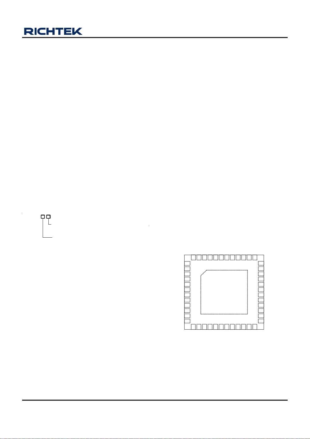
Pin Configurations
(TOP VIEW)
EN
PGOOD
VID5
VID4
VID3/SVC
PWROK
RT
FBRTN
FBRTN_NB
FB_NB
COMP_NB
ISP_NB
ISN_NB
ADJ
OFS
COMP
FB
VID2/SVD
VID1/PVI
VID0/VFIXEN
VCC12_NB
1
2
3
4
5
6
7
8
9
10
11
12
IMAX
IMAX_NB
ISN1
ISP1
GND
ISN2
ISP2
ISN3
ISP3
ISN4
49
LGATE_NB
ISP4
UGATE_NB
PHASE_NB
373839404142434445464748
242322212019181716151413
PS
VCC5
BOOT_NB
36
BOOT1
35
34
UGATE1
33
PHASE1
32
LGATE1
31
VCC12
30
LGATE2
29
PHASE2
28
UGATE2
27
BOOT2
26
PWM3
25
PWM4
WQFN-48L 7x7
DS8855-00 July 2008 www.richtek.com
1
Page 2
RT8855
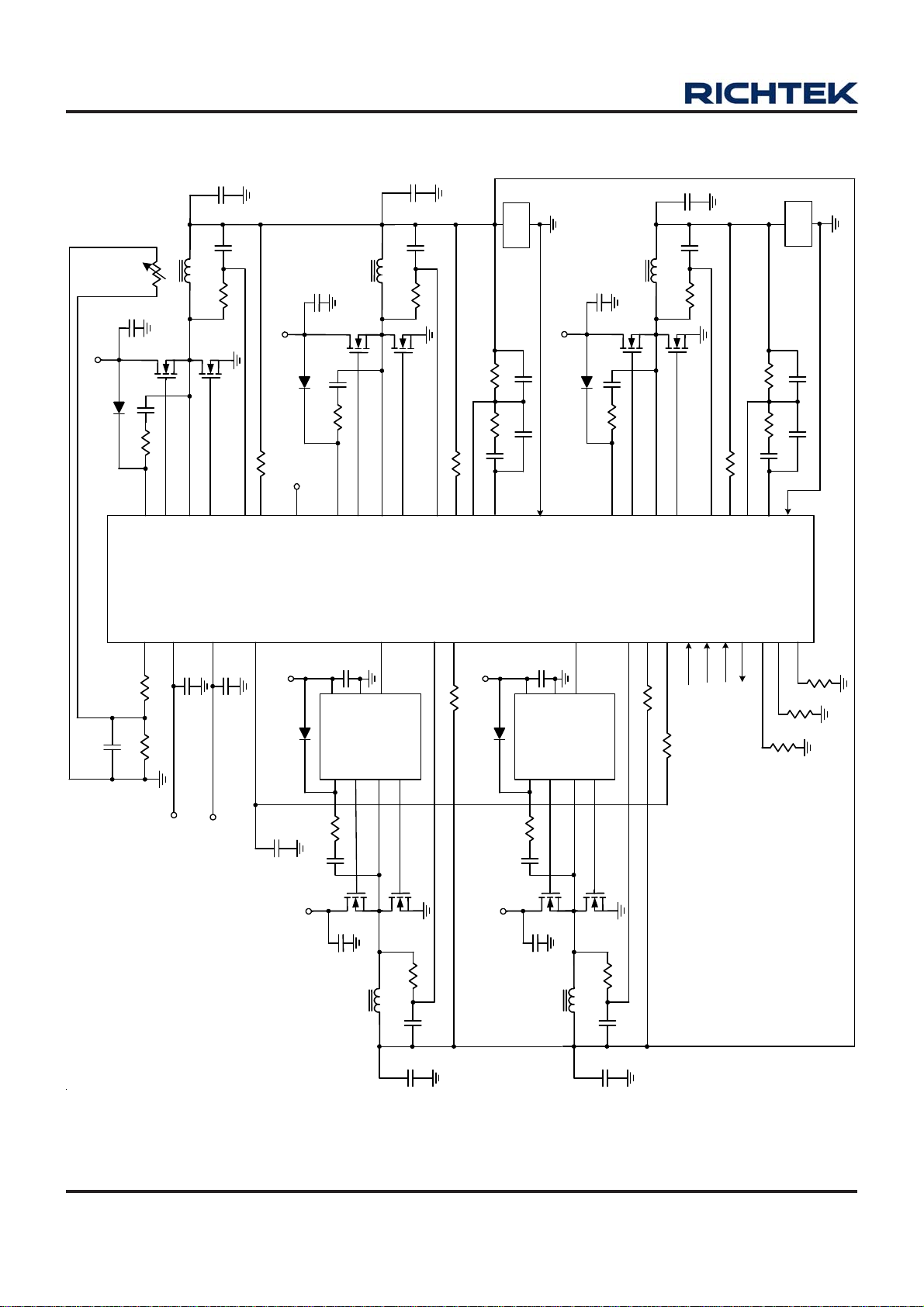
Typical Application Circuit
LOAD
C
1
T
L
N
V
2
V
2
1
5
3
1
T
O
O
B
5
5
8
8
T
R
J
D
A
9
2
3
4
3
3
3
1
1
1
E
E
E
T
T
S
A
A
A
G
G
H
L
P
U
B
N
_
2
2
1
1
C
C
C
C
V
V
1
0
3
4
1
3
5
6
1
2
1
1
1
P
S
I
4
2
S
N
P
S
I
5
C
C
V
V
2
1
2
L
V
2
1
8
0
9
8
7
2
2
T
O
O
B
3
2
2
2
2
2
E
E
E
T
T
S
A
A
A
H
G
G
L
P
U
3
M
W
P
6
2
7
2
1
2
P
S
I
3
P
S
I
0
2
1
1
1
2
B
N
F
S
I
3
N
S
I
9
1
V
2
1
3
1
P
N
T
M
R
O
B
C
F
4
M
W
P
5
2
2
L
9
8
7
6
3
3
3
B
B
B
N
N
N
_
_
_
T
E
E
T
S
O
A
A
O
G
H
B
P
U
4
4
N
P
S
S
I
I
1
2
2
2
7
3
B
N
_
E
T
A
G
L
]
0
:
5
[
S
D
F
I
V
O
0
1
1
4
o
t
6
4
5
8
B
B
B
N
N
N
_
_
_
B
P
N
F
S
S
I
I
K
D
O
O
R
O
G
W
N
P
P
E
7
8
1
4
4
LOAD
6
4
B
B
N
N
_
_
P
N
T
M
R
O
B
C
F
B
N
_
X
X
A
A
T
M
M
I
R
I
4
2
3
1
1
VCC
GND
BOOT
UGATE
V
V
2
2
1
1
V
2
1
2
L
PWM
PHASE
LGATE
9
1
6
9
T
R
VCC
GND
BOOT
UGATE
V
2
1
2
L
PWM
PHASE
LGATE
9
1
6
9
T
R
S
F
O
R
DS8855-00 July 2008www.richtek.com
2
Page 3

RT8855
Table 1. 7-bit VID Code Table for AM2+ CPU (Serial)
SVID[6:0] Voltage SVID[6:0] Voltage SVID[6:0] Voltage SVID[6:0] Voltage
0000000 1.5500 0100000 1.1500 1000000 0.7500 1100000 0.3500
0000001 1.5375 0100001 1.1375 1000001 0.7375 1100001 0.3375
0000010 1.5250 0100010 1.1250 1000010 0.7250 1100010 0.3250
0000011 1.5125 0100011 1.1125 1000011 0.7125 1100011 0.3125
0000100 1.5000 0100100 1.1000 1000100 0.7000 1100100 0.3000
0000101 1.4875 0100101 1.0875 1000101 0.6875 1100101 0.2875
0000110 1.4750 0100110 1.0750 1000110 0.6750 1100110 0.2750
0000111 1.4625 0100111 1.0625 1000111 0.6625 1100111 0.2625
0001000 1.4500 0101000 1.0500 1001000 0.6500 1101000 0.2500
0001001 1.4375 0101001 1.0375 1001001 0.6375 1101001 0.2375
0001010 1.4250 0101010 1.0250 1001010 0.6250 1101010 0.2250
0001011 1.4125 0101011 1.0125 1001011 0.6125 1101011 0.2125
0001100 1.4000 0101100 1.0000 1001100 0.6000 1101100 0.2000
0001101 1.3875 0101101 0.9875 1001101 0.5875 1101101 0.1875
0001110 1.3750 0101110 0.9750 1001110 0.5750 1101110 0.1750
0001111 1.3625 0101111 0.9625 1001111 0.5625 1101111 0.1625
0010000 1.3500 0110000 0.9500 1010000 0.5500 1110000 0.1500
0010001 1.3375 0110001 0.9375 1010001 0.5375 1110001 0.1375
0010010 1.3250 0110010 0.9250 1010010 0.5250 1110010 0.1250
0010011 1.3125 0110011 0.9125 1010011 0.5125 1110011 0.1125
0010100 1.3000 0110100 0.9000 1010100 0.5000 1110100 0.1000
0010101 1.2875 0110101 0.8875 1010101 0.4875 1110101 0.0875
0010110 1.2750 0110110 0.8750 1010110 0.4750 1110110 0.0750
0010111 1.2625 0110111 0.8625 1010111 0.4625 1110111 0.0675
0011000 1.2500 0111000 0.8500 1011000 0.4500 1111000 0.0500
0011001 1.2375 0111001 0.8375 1011001 0.4375 1111001 0.0375
0011010 1.2250 0111010 0.8250 1011010 0.4250 1111010 0.0250
0011011 1.2125 0111011 0.8125 1011011 0.4125 1111011 0.0125
0011100 1.2000 0111100 0.8000 1011100 0.4000 1111100 OFF
0011101 1.1875 0111101 0.7875 1011101 0.3875 1111101 OFF
0011110 1.1750 0111110 0.7750 1011110 0.3750 1111110 OFF
0011111 1.1625 0111111 0.7625 1011111 0.3625 1111111 OFF
DS8855-00 July 2008 www.richtek.com
3
Page 4

RT8855
Table 2. 6-bit VID Code Table for AM2 CPU (Parallel)
VID[5:0] Voltage VID[5:0] Voltage VID[5:0] Voltage VID[5:0] Voltage
000000 1.5500 010000 1.1500 100000 0.7625 110000 0.5625
000001 1.5250 010001 1.1250 100001 0.7500 110001 0.5500
000010 1.5000 010010 1.1000 100010 0.7375 110010 0.5375
000011 1.4750 010011 1.0750 100011 0.7250 110011 0.5250
000100 1.4500 010100 1.0500 100100 0.7125 110100 0.5125
000101 1.4250 010101 1.0250 100101 0.7000 110101 0.5000
000110 1.4000 010110 1.0000 100110 0.6875 110110 0.4875
000111 1.3750 010111 0.9750 100111 0.6750 110111 0.4750
001000 1.3500 011000 0.9500 101000 0.6625 111000 0.4625
001001 1.3250 011001 0.9250 101001 0.6500 111001 0.4500
001010 1.3000 011010 0.9000 101010 0.6375 111010 0.4375
001011 1.2750 011011 0.8750 101011 0.6250 111011 0.4250
001100 1.2500 011100 0.8500 101100 0.6125 111100 0.4125
001101 1.2250 011101 0.8250 101101 0.6000 111101 0.4000
001110 1.2000 011110 0.8000 101110 0.5875 111110 0.3875
001111 1.1750 011111 0.7750 101111 0.5750 111111 0.3750
DS8855-00 July 2008www.richtek.com
4
Page 5

RT8855
Functional Pin Description
Pin No. Pin Name Pin Function
1 PWROK PWROK Input Signal.
2 RT Connect this pin to GND by a resistor to adjust frequency.
3 FBRTN Remote sense ground for CORE.
4 FBRTN_NB Remote sense ground for NB.
5 FB_NB Inverting input of error-amp for NB.
6 COMP_NB Output of error-amp and input of PWM comparator for NB.
7 ISP_NB Positive current sense pin of NB
8 ISN_NB Negative current sense pin of NB
9 ADJ
10 OFS
11 COMP Output of error-amp and input of PWM comparator of V
12 FB Inverting input of error-amp of V
13 IMAX_NB Connect this pin to GND by a resistor to set OCP of NB.
14 IMAX Connect this pin to GND by a resistor to set OCP of VCORE.
15, 17, 19, 21 ISN1, ISN2, ISN3 , ISN4 Negative current sense pin of channel 1, 2, 3 and 4.
16, 18, 20, 22 ISP1, ISP2, ISP3, ISP4 Positive current sense pin of channel 1, 2, 3 and 4.
23 PS Power Saving Mode Selection Pin.
24 VCC5
25,26 PWM4, PWM3 PWM output for channel 4 and channel 3.
27, 35, 36 BOOT2, BOOT1, BOOT_NB Bootstrap supply for channel 2 and channel 1 and NB.
28, 34, 37 UGATE2, UGATE1, UGATE_NB Upper gate driver for c hannel 2 and channel 1 and NB.
29, 33, 38 PHASE2, PHASE1, PHASE_NB Switching node of channel 2 and channel 1 and NB.
30, 32, 39 LGATE2, LGATE1, LGATE_NB Lower gate driver for channel 2 and channel 1 and NB.
31, 40 VCC12, VCC12_NB IC power supply. Connect this pin to 12V.
41 VID0/VFIXEN
42 VID1/PVI
43 VID2/SVD
44 VID3/SVC
45, 46 VID4, VID5 PVI Mode : Used as voltage identification input for DAC.
47 PGOOD Power Good Indicator (open drain).
48 EN Enable Input Signal.
Exposed pad
(49)
GND
Connect this pin to GND by a resistor to set load line of
VCORE.
Connect this pin to GND/5VCC by a resistor to set no-load
offset voltage of V
Output of internal 5V regulator for control circuits power supply.
Connect this pin to GND by a ceramic capacitor larger than 1uF.
PVI Mode : Used as voltage identification i nput for DAC.
SVI Mode : Functions as VFIXEN selection input.
This pin selects PVI/SVI mode based on the state of this pin
prior to EN signal.
PVI Mode : Used as voltage identification i nput for DAC.
PVI Mode : Used as voltage identification i nput for DAC.
SVI Mode : Serial data input.
PVI Mode : Used as voltage identification i nput for DAC.
SVI Mode : Serial clock input.
Reference Ground for the IC. The exposed pad must be
soldered to a large PCB and connected to GND for maximum
power dissipation.
CORE
.
.
CORE
CORE
.
DS8855-00 July 2008 www.richtek.com
5
Page 6
RT8855
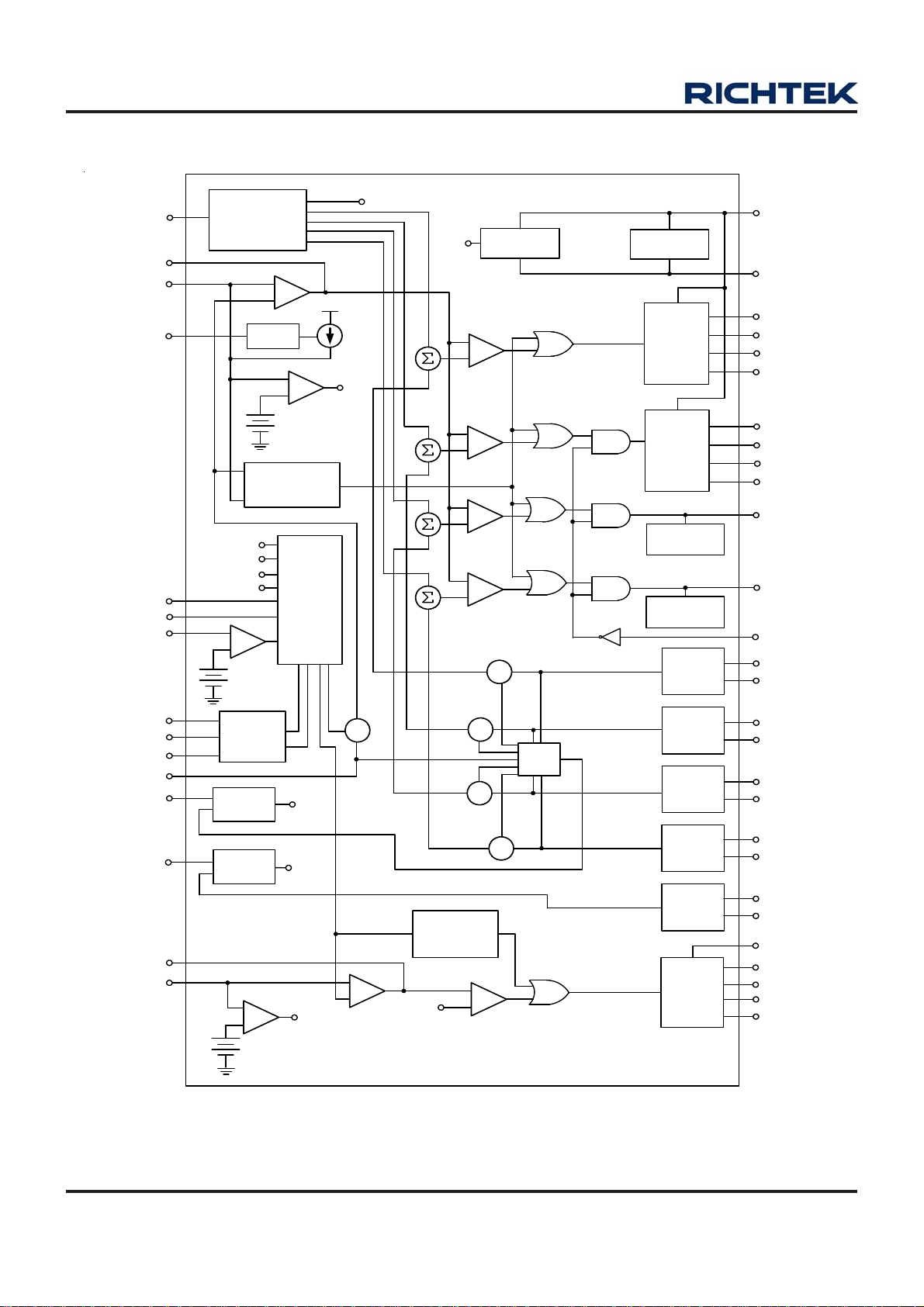
Function Block Diagram
RT
COMP
FB
OFS
PGOOD
PWROK
EN
VIDOFF
+
Modulator
Waveform
Generator
Offset
+
Transient
Response
Enhancement
OV
OC
POR
+
-
1.25V
-
EA
+
+
-
1.8V
Soft Start
and
Fault
Logic
RAMP_NB
OV
POR
+
-
+
-
+
-
+
-
Power-On
Reset
+
-
Regulator
I_SEN1
5V
MOSFET
Driver
MOSFET
Driver
CH3_EN
Detector
CH4_EN
Detector
CH1
Current
SENSE
VCC12
VCC5
BOOT1
UGATE1
PHASE1
LGATE1
BOOT2
UGATE2
PHASE2
LGATE2
PWM3
PWM4
PS
ISP1
ISN1
VID5 to VID 0
FBRTN
FBRTN_NB
ADJ
IMAX
IMAX_NB
COMP_NB
FB_NB
Table
Generator
OC
Detection
OC_NB
Detection
+
1.8V
VID
+
-
OC
OC_NB
OV_NB
+
-
-
EA
+
Enhancement
RAMP_NB
Transient
Response
+
I_SEN2
-
AVG
-
+
-
+
+
-
I_SEN3
I_SEN4
I_SENNB
CH2
Current
SENSE
CH3
Current
SENSE
CH4
Current
SENSE
NB
Current
SENSE
MOSFET
Driver
ISP2
ISN2
ISP3
ISN3
ISP4
ISN4
ISP_NB
ISN_NB
VCC12_NB
BOOT_NB
UGATE_NB
PHASE_NB
LGATE_NB
DS8855-00 July 2008www.richtek.com
6
Page 7

RT8855
Absolute Maximum Ratings (Note 1)
z Supply Input Voltage------------------------------------------------------------------------------------------------------ −0.3V to 15V
z BOOTx to PHASEx------------------------------------------------------------------------------------------------------- −0.3V to 15V
z BOOTx to GND
DC----------------------------------------------------------------------------------------------------------------------------- −0.3V to 30V
<200ns ----------------------------------------------------------------------------------------------------------------------- −0.3V to 42V
z PHASEx to GND
DC----------------------------------------------------------------------------------------------------------------------------- −2V to 15V
<200ns ----------------------------------------------------------------------------------------------------------------------- −5V to 30V
z Input/Output V oltage or I/O V oltage----------------------------------------------------------------------------------- −0.3V to 7V
z Power Dissipation, P
D
WQFN−48L 7x7------------------------------------------------------------------------------------------------------------ 3.226W
z Package Thermal Resistance (Note 4)
WQF N-48L 7x7, θJA------------------------------------------------------------------------------------------------------- 31°C/W
z Junction T emperature----------------------------------------------------------------------------------------------------- 150°C
z Lead Temperature (Soldering, 10 sec.)------------------------------------------------------------------------------- 260°C
z Storage T emperature Range -------------------------------------------------------------------------------------------- −65°C to 150°C
z ESD Susceptibility (Note 2)
HBM (Human Body Mode) ---------------------------------------------------------------------------------------------- 2kV
MM (Ma chine Mode)------------------------------------------------------------------------------------------------------ 200V
@ T
= 25°C
A
Recommended Operating Conditions (Note 3)
z Supply V oltage, VCC12-------------------------------------------------------------------------------------------------- 12V ± 10%
z Junction T emperature Range-------------------------------------------------------------------------------------------- −40°C to 125°C
z Ambient T emperature Range--------------------------------------------------------------------------------------------
0°C to 70°C
Electrical Characteristics
(VCC12 = 12V, GND = 0V, TA = 25°C, unless otherwise specified)
Parameter Symbol Conditions Min Typ Max Unit
VCC Supply Input
VCC12 Supply Voltage V
VCC12 Supply Current I
VCC12_NB Supply Voltage V
VCC12_NB Supply Current I
VCC5 Power
VCC5 Supply Voltage V
VCC5 Output Sourcing I
Power-On Reset
VCC12 Rising Threshold V
VCC12 Hysteresis V
Input Thr eshold
Enable Input High Threshold V
Enable Input Low Threshold V
VCC12
VCC12_NB
VCC5
10.8 12 13.2 V
VCC12
-- 10 -- mA
VCC12_NB
10.8 12 13.2 V
-- 5 -- mA
I
VCC5
= 10mA 4.9 5 5.1 V
LOAD
10 -- -- mA
VCC12TH
VCC12HY
ENHI
ENLO
VCC12 Rising 9.2 9.6 10 V
VCC12 Falling -- 0.9 -- V
EN Rising 2 -- -- V
EN Falling -- -- 0.8 V
To be continued
DS8855-00 July 2008 www.richtek.com
7
Page 8

RT8855
Parameter Symbol Conditions Min Typ Max Unit
PWROK Input High Threshold V
PWROK Input Low Threshold V
VI D5 to VID0 Rising Threshold V
VID5 to VID0 Hysteresis V
VID5 to VID0 Pull-Down
Current
Refer en ce Voltag e a ccura cy
PWROK Rising 2 -- -- V
POKHI
PWROK Falling -- -- 0.8 V
POKLO
VID5 to 0
VID5 to 0 HYS
I
VID5 to 0
VID5 to VID0 Rising 0.75 0.8 0.85 V
V
VID5 to VID0 Falling -- 25 -- mV
VID5 to 0
= 1.5V -- 16 30 uA
1V to 1. 55V −0.5 -- +0.5 %
DAC Accuracy
0.8V to 1V −8 -- +8 mV
0.5V to 0.8V −10 -- +10 mV
Error Amplifier
DC Gain ADC No Load -- 80 -- dB
Gain-Bandwidth GBW C
Slew Rate SR C
Output Voltage Range V
R
COMP
= 10pF -- 10 -- MHz
LOAD
= 10pF 10 - - -- V/ us
LOAD
= 47 kΩ 0.5 -- 3.6 V
LOAD
Power Good
Over-Voltage Threshold V
Under-Voltage Threshold V
Over-Voltage Threshold_NB V
Under-Voltage Threshold_NB V
Power Good Low Voltage V
PGOOD-OV
PGOOD-UV
PGOOD-OV_NB
PGOOD-UV_NB
PGOOD
FB Rising
FB Falling
I
FB_NB Rising
FB_NB Falling
PGOOD
= 4mA -- -- 0.4 V
VDAC
+210mV
VDAC
−330mV
VDAC
+210mV
VDAC
−330mV
VDAC
+240mV
VDAC
−300mV
VDAC
+240mV
VDAC
−300mV
VDAC
+270mV
VDAC
−270mV
VDAC
+270mV
VDAC
−270mV
V
V
V
V
Current Sense Amplifier
Max Current I
Input Offset Voltage V
GMMAX
−2 0 +2 mV
OSCS
CSP
Sink Current fr om CSN
100 -- -- uA
= 1.3V
V
Oscillator
Running Frequency f
Ramp Amplitude V
R
OSC
-- 1.6 -- V
RAMP
= 40kΩ 270 300 330 kHz
RT
Soft Start
Soft Start Slew Rate SRSS Slew Rate 2.5 3.25 4 mV/us
VID change Slew Rate SR
Slew Rate 2.5 3.25 4 mV/us
VID
Protection
V
Sweep FB Voltage 1.7 1.8 1.9 V
Over-Voltage Threshold
8
OVP
V
OVP_NB
Sweep FB_NB Voltage 1.7 1.8 1.9 V
To be continued
DS8855-00 July 2008www.richtek.com
Page 9

RT8855
Parameter Symbol Conditions Min Typ Max Unit
R
I
OCP
V
R
Over-Current Threshold
IMAX
I
OCP_NB
V
IMAX_NB
R
R
Gate Driver
UGATE Drive Source R
UGATE Drive Sink R
LGATE Drive Source R
LGATE Drive Sink R
Note 1. Stresses listed as the above “Absolute Maximum Ratings” may cause permanent damage to the device. These are for
stress ratings. Functional operation of the device at these or any other conditions beyond those indicated in the
operational sections of the specifications is not implied. Exposure to absolute maximum rating conditions for extended
periods may remain possibility to affect device reliability.
Note 2. Devices are ESD sensitive. Handling precaution is recommended.
Note 3. The device is not guaranteed to function outside its operating conditions.
Note 4. θ
is measured in the natural convection at TA = 25°C on a effective single layer thermal conductivity test board of
JA
JEDEC thermal measurement standard.
UGATEsr
UGATEsk
LGATEsr
LGATEsk
V
250mA Sink Current -- 0.9 -- Ω
= 40k Ω 68 80 92 uA
IMAX
= 40k Ω 1.44 1.6 1.76 V
IMAX
IMAX_NB
IMAX_NB
BOOT − PHASE = 8V
250mA Source Current
BOOT − PHASE = 8V
250mA Sink Current
LGATE
= 40kΩ 68 80 92 uA
= 40kΩ 1.44 1.6 1.76 V
-- 1 -- Ω
-- 1 -- Ω
= 8V -- 1 -- Ω
DS8855-00 July 2008 www.richtek.com
9
Page 10
RT8855
Application Information
The RT8855 is a dual output PWM controller supports
hybrid power control of AMD processors which operate
from either a 6-bit parallel VID interface (PVI) or a serial
VID interfa ce (SVI). One of the outputs is a 4/3/2/1-pha se
PWM controller with two integrated MOSFET drivers to
support CPU core voltage (V DD) and a nother is a singlephase buck controller with a n integrated MOSFET driver
to power North-Bridge (NB) chi pset (VDDNB) in SVI mode.
In PVI mode, only multiphase PWM controller is active
for single-plane V DD only processor.
Richtek's proprietary Burst Tra nsient Response(BTRTM),
provides fastest initi al response to high di/dt load tran sients
and less bulk a nd cera mic output ca pa citance is required
to meet transient regulation specifications. The RT8855
incorporates differential voltage sensing, continuous
inductor DCR pha se current sensing, progra mmable loadline voltage positioning and offset voltage to provide high
accura cy regulated power for both V DD and V DDNB. While
VDDNB is enabled in SVI mode, it will be automatically
phase-shifted with respect to the CPU Core phases in
order to reduce the total input RMS current amount.
CPU_TYPE Detection and System Start-Up
At system Start-up, on the rising-edge of EN signal,
RT8855 monitors the status of VID1 a nd latches the PVI
mode (VID1 = 1) or SVI mode (VID1 = 0).
PVI Mode
PVI is a 6-bit-wide parallel interface used to address the
CPU Core section reference. According to the selected
code, the device sets the Core section reference and
regulates its output voltage according to Table 2. In this
mode, NB section is kept in high i mpedance. Furthermore,
PWROK information is ignored as well since the signal
only applies to the SVI protocol.
SVI Mode
SVI is a two wire, Clock and Data, bus that connect a
single master (CPU) to one slave (R T8855). The master
initiates and terminates SVI transactions and drives the
clock, SVC, and the data, SV D, during a tra nsaction. The
slave receives the SVI transa ctions a nd acts a ccordingly .
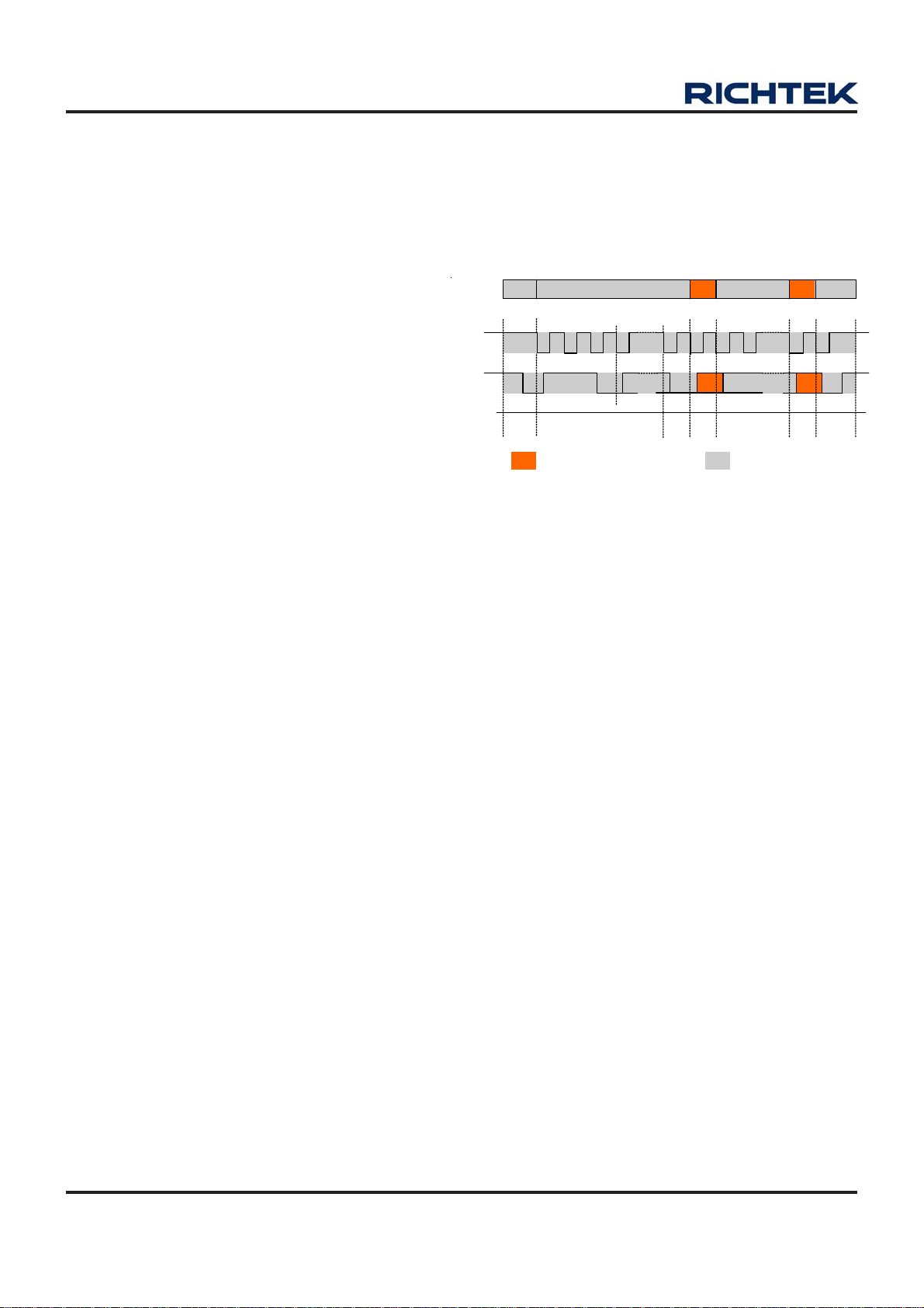
SVI wire protocol is based on fast-mode I2C a s shown in
Figure1. SVI interface also consider two additional sign als
needed to manage the system start-up. These signals
are EN a nd PWROK. The device asserts a PGOOD signal
if the output voltages are in regulation.
Start Slave Addressing + W ACK ACKData Phase Stop
SVC
SVD
65430 760
ACK ACK
110b
Start
Slave Addressing
(7 Clocks)
BUS Driven by RT8855 BUS Driven by Master (CPU)
Write
(1Ck)
ACK
(1Ck)
Data Phase
(8 Clocks)
ACK
(1Ck)
Figure 1. SVI Communication-Send Byte
Set VID Command
The Set VID Command is defined as the command
sequence that the CPU issues on the SVI bus to modify
the voltage level of the Core section and NB section, a s
shown is Figure 1. During a Set VID Command, the
processor sends the start (Start) sequence followed by
the address of the Section which the Set VID Command
applies. The processor then sends the write (WRITE) bit.
After the write bit, The V oltage Regulator (V R) sends the
acknowledge (ACK) bit. The processor then sends the
VID bits code during the data phase. The VR sends the
acknowledge (ACK) bit after the data phase. Finally, the
processor sends the stop (Stop) sequence. After the VR
has detected the stop, it performs an On-the-Fly VID
transition for the addressed section(s). Refer to Table 3
for the details of SVI send byte.
RT8855 is able to manage individual power off for both
VCORE and NB sections. The CPU may issue a serial
VID comma nd to power off or power on one section while
the other one remains powered. In this ca se, the PGOOD
signal remains a sserted.
Stop
10
DS8855-00 July 2008www.richtek.com
Page 11
RT8855
Table 3. SVI Send Byte-Address and Data Phase
Description / Example
bits Description
Address Phase
6 : 4 Always 110b
3 Not Applicable, ignored.
2 Not Applicable, ignored.
CORE Section. (Note)
1
If set then the following data byte contains the
VID code for CORE Section.
NB Section. (Note)
0
If set then the following data byte contains the
VID code for NB Section.
Data Phase
7
PSI_L Flag (Active Low). When asserted, the
VR is allowed to enter Power-Saving Mode.
6 : 0 VID Code.
Note : Assertion in both bit 1 and 0 will address the VID
code to both CORE and NB simultaneously.
Example :
SVI Address
Bits [6 : 0]
Description
1100_000 Should be ignored.
1100_001 Set VID on VDDNB.
1100_110 Set VID on VDD0 and VDD1.
1100_100 Set VID on VDD1.
1100_010 Set VID on VDD0 or VDD (uniplane).
1100_111
Set VID on VDDNB, VDD0 and
VDD1.
Table 4. V_FIX Mode and Pre-PWROK Metal VID
Output Voltage (V)
SVC SVD
Pre-PWROK
Metal VID
V_FIX Mode
0 0 1.1V 1.4V
0 1 1.0V 1.2V
1 0 0.9V 1.0V
1 1 0.8V 0.8V
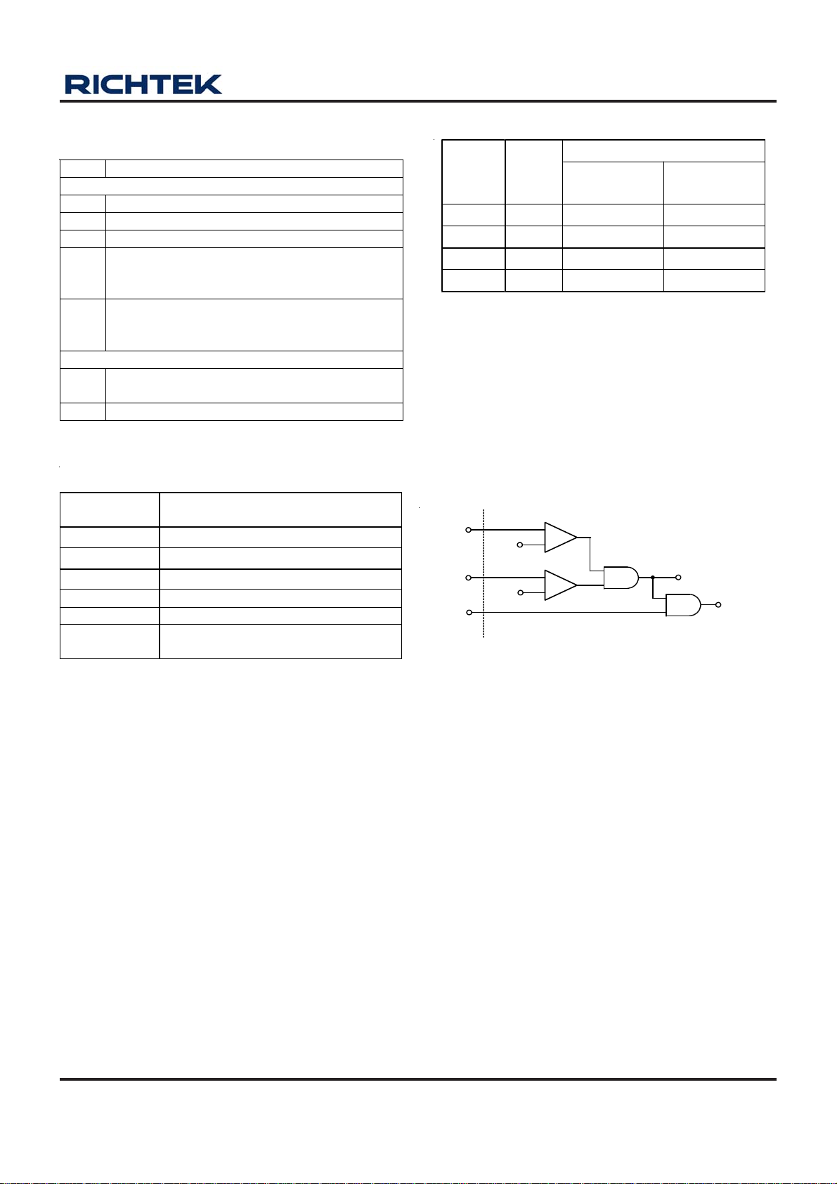
Power Ready Detection
During start-up, RT8855 will detect VCC12, VCC5 and
EN signal. Figure 2 shows the power ready detection
circuit. When VCC12 > 9.6V and VCC5 > 4.6V, POR
(Power On Reset) will go high. POR is the internal signal
to indicate all input powers are ready to let RT8855 and
the companioned MOSFET drivers to work properly . When
POR = L, RT8855 will turn off both high side and low side
MOSFETs.
VCC12
9.6V
VCC5
4.6V
EN
CMP
+
-
CMP
+
-
POR
Chip Enable
Figure 2. Circuit for Power Ready Detection
PWROK De-a ssertion
PWROK stays low after EN signal is asserted, and the
controller regulates all the planes according to the PrePWROK Metal VID.
PGOOD is de-a sserted a s long as Pre-PW ROK Metal VID
voltage is out of the initial voltage specifications.
V_FIX Mode Function
Anytime the pin VID0/VFIXEN is pulled high, the controller
enters V -FIX mode. When in V_FIX mode, both VCORE
and NB section voltages are governed by the information
shown in T a ble 4. Regardless of the state of PWROK, the
device will work in SVI mode. SVC and SV D are considered
as static VID and the output voltage will be changed
according to their status. Dynamic SVC/SVD-change
management is provided in this condition. V_FIX mode is
intended for system debug only .
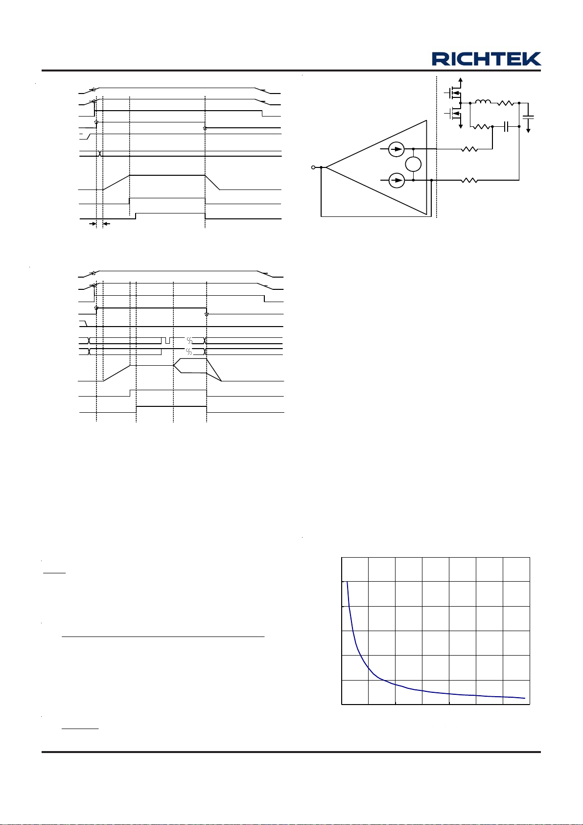
Power-Up Sequencing
Figure 3 and 4 are the power-up sequencing diagram of
RT8855. Once power_on_reset is valid (POR = H), on the
rising edge of the EN signal, the RT8855 detects the VID1
pin and determine to operate either in SVI or PVI mode.
Figure3 shows the PVI-mode power sequence, the
controller stays in T1 state waiting for valid parallel VID
code sent by CPU. After rec eiving valid parallel VID code,
VCORE continues ramping up to the specified voltage
according to the VID code in T2 state. Figure 4 shows the
SVI-mode power sequence, the controller samples the
two serial VID pins, SVC and SVD. Then, the controller
stores this value as the boot VID that is the so-called
“Pre-PWROK Metal VID” in T1 state. After the processor
starts with boot VID voltages, PWROK is asserted and
the processor initializes the serial VI D interfa ce in T2 state.
The processor uses the serial VID interfa ce to issue VID
commands to move the power pla nes from the boot VID
values to the dual power planes in T3 state.
DS8855-00 July 2008 www.richtek.com
11
Page 12
RT8855
9.6V
VCC12
4.6V
VCC5
POR
EN
(6-bits)
VDD
xx
xx
T1
Valid
T2
VID(1)/PVI
PVI mode
PGOOD
PWROK
Figure 3. PVI-Mode Power-sequencing Di agram
9.6V
VCC12
4.6V
VCC5
POR
EN
SVC
SVD
xx
xx
xx
Vboot
T1 T2 T3
Valid
Valid
VID(1)/PVI
VDD or
VDDNB
PGOOD
PWROK
Figure 4. SVI-Mode Power-sequencing Diagra m
CORE Section- Output Current Sensing
8.7V
4.2V
8.7V
4.2V
L
DCR
C
CSA: Current Sense Amplifier
235nA
V
I
X
OFS_CSA
235nA
R
R
CSP
ISP
+
+
-
-
ISN
R
CSN
S
S
Figure 5. Current Sensing Circuit.
CORE Section- Phase Dete ction
The number of the operational pha ses is determined by
the internal circuitry that monitors the ISNx voltages during
start up. Normally, the RT8855 operates as a 4-phase
PWM controller. Pull ISN4 and ISP4 to 5VCC programs
3-phase operation, pull ISN3 a nd ISP3 to 5VCC progra ms
2-phase operation, and pull ISN2 and ISP2 to 5VCC
programs 1-pha se operation. RT8855 detects the voltage
of ISN4, ISN3 and ISN2 at rising edge of POR. At the
rising edge, RT8855 detects whether the voltage of ISN4,
ISN3 and ISN2 are higher tha n “VCC5-1V” respectively
to decide how many phases should be active. Phase
detection is only active during start up. Once POR = high,
the number of operational phases is determined and
latched.
The RT8855 provides a low input offset current-sense
amplif ier (CSA) to monitor the continuous output current
of each phase for V
. Output current of CSA (IX[n]) is
CORE
used for current balance and active voltage position as
shown in Figure 5. In this inductor current sensing topology ,
RS and CS must be set according to the equation below :
L
RC
=×
DCR
SS
Then the output current of CSA will follow the equation
below :
[I DCR V 235nA (R R )]
×− + × −
LOFS-CSA CSPCSN
I
=
X
R
CSN
235nA is the typical value of the CSA input offset current.
V
OFS-CSA
(R
is the input offset. Usually, “V
− R
CSP
)” is negligible except at very light load and
CSN
OFS-CSA
+ 235nA x
the equation can be simplified as the equation below :
I DCR
×
L
I
=
X
R
CSN
12
CORE Section- Switching Frequency
Connect a resistor (RT) from the RT pin to GND ca n program
the switching frequency of each phase. Figure 6 shows
the relationship between the resistance and switching
frequency .
1200
1000
800
600
400
Frequency ( kHz)
200
0
0 40 80 120 160 200 240 280
Frequency vs. R
RRT (k ohm)
(kΩ)
RT
Figure 6. RRT vs. Phase switching Frequency.
DS8855-00 July 2008www.richtek.com
Page 13
RT8855
A
A
CORE Section- Differential Output Voltage Sensing
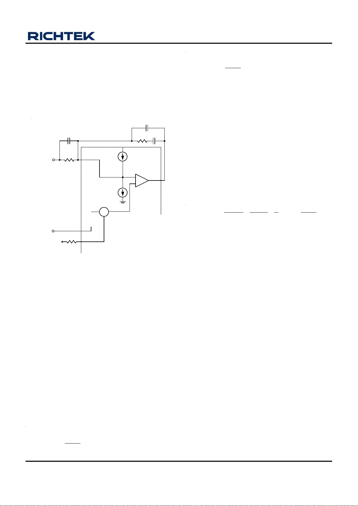
The RT8855 uses differential voltage sensing by a high
gain low offset ErrorAmp a s shown in Figure 7. Connect
the negative on-die CPU remote sense pin to FBRTN.
Connect the positive on-die remote sense pin to FB with
a resistor (RFB) The ErrorAmp compares EAP
( = V
− V
DAC
ADJ
V
CCP
(Positive remote
sense pin of CPU)
(Negative remote
sense pin of CPU)
V
CCN
) with the VFB to regulate the output voltage.
C2
C
FB
R
FB
FB
V
FBRTN
R
ADJ
ADJ
+
DAC
-
I
OFSN
I
OFSP
+
-
EAP
C1
R1
-
COMP
EA
+
VIR9uR
0.4 9u R
=×−×
OFSP OFSP FB ADJ
R
R
FB
OFS
DJ
=× −×
CORE Section- Programmable Load-line
Output current of CSA is summed and averaged in
RT8855. Then 0.5Σ (IX[n]) is sent to ADJ pin. Because
Σ IX[n] is a PTC (Positive T emperature Coef ficient) current,
an NTC (Negative Temperature Coefficient) resistor is
needed to connect ADJ pin to GND. If the NTC resistor is
properly selected to compensate the temperature
coefficient of IX[n], the voltage on ADJ pin will be
proportional to I
the positive input of ErrorAmp is “V
follow “V
DAC
decreasing linearly with I
without temperature effect. In RT8855,
OUT
− V
ADJ
”. V
− V
DAC
”, too. Thus, the output voltage
ADJ
is obtained. The loadline is
OUT
OUT
will
defined a s :
VV R
ΔΔ
LL(loadline) DCR
OUT ADJ ADJ
===××
II2R
ΔΔ
OUT OUT CSN
Briefly, the resistance of R
loadline. The temperature coefficient of R
1
sets the resistance of
ADJ
compensates
ADJ
the temperature effect of loadline.
Figure 7. Circuit for VCORE Differential Sensing a nd No
load Offest.
CORE Section- No-Load Offset
In Figure 7, I
offset. Either I
Connect a resistor from OFS pin to G ND to a ctivate I
I
flows through RFB from FB pin to V
OFSN
negative no-load offset voltage (V
Connect a resistor from OFS pin to 5VCC to activate I
I
flows through RFB from the V
OFSP
case, positive no-loa d offset voltage (V
Beside I
OFSN
OFSP
OFSP
and I
and I
or I
OFSP
are used to generate no-load
OFSN
is active during normal operation.
OFSN
. In this case,
CCP
) is generated.
OFSN
to FB pin. In this
CCP
) is generated.
OFSP
, the RT8855 generates another DC
OFSN
OFSP
current for initial no-load negative offset. A DC current
source will continuously inject typical 9uA current into
the resistors connected to ADJ pin, Therefore, the ef fect
of this 9uA current source and ADJ resistors should
counted into the calculation of no-load offset :
VIR9uR
0.4 9u R
=×+×
OFSN OFSN FB ADJ
R
=× +×
R
FB
OFS
DJ
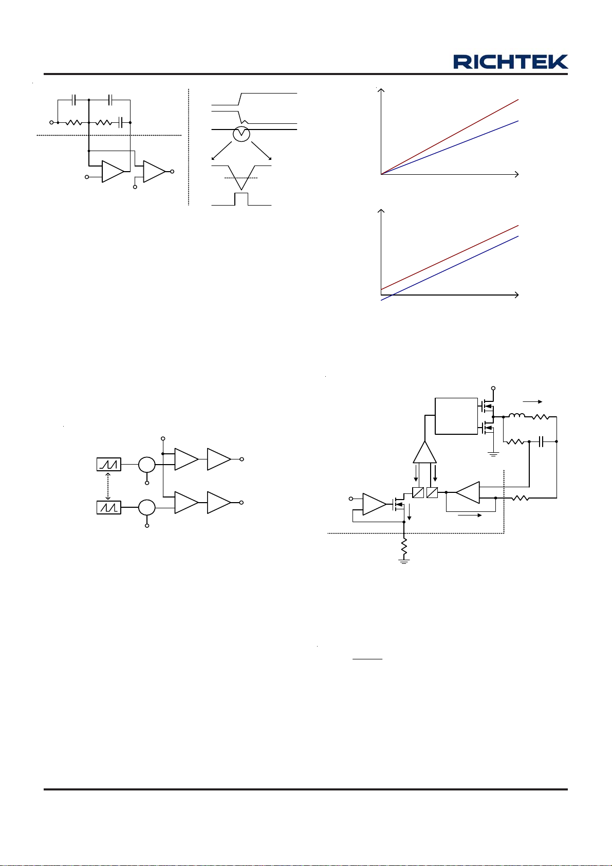
CORE Section- Load T ra n sient Quick Response
In steady state, the voltage of VFB is controlled to be very
close to V
to heavy load could cause VFB lower than V
. While a load step tra n sient from light loa d
EAP
EAP
tens of mV. In prior design, owing to limited control
bandwidth, controller is hard to prevent V
.
during quick load tran sient from light load to heavy loa d.
OUT
RT8855 buit in proprietary Burst Transient Response
TM
(BTR
.
comparing VFB and V
“V
) technology, that detects load transient by
. If VFB suddenly drops below
EAP
− VOR”, V
EAP
is a predetermined voltage. The quick
QR
response indicator QR rises up. When QR = high, RT8855
turns on all high side MOSFETs and turn off all low side
MOSFETs. The sensitivity of quick response can be
adjusted by the values of CFB and RFB. Smaller RFB and/
or larger CFB will make QR ea sier to be trigger . Figure8 is
the circuit and typical waveforms.
by several
undershoot
DS8855-00 July 2008 www.richtek.com
13
Page 14
RT8855
C
FB
R
V
OUT
R1
FB
FB COMP
C2
C1
V
I
OUT
OUT
FB
I1
I2
EAP = V
DAC
- V
+
ADJ
EAP - V
QR
+
QR
FB
QR
= V
= V
EAP
Figure 8. Load Tr ansient Quick Respon se
CORE Section- Current Balance
In Figure9, IX[n] is the current signal which is proportional
to the current flowing through channel n. The current error
signals I
[n] ( = IX[n] − A V G(IX[n])) are used to raise or
ERR
lower the valley of internal sawtooth waveforms (EAMP[1]
to RAMP[n]) which are compared with ErrorAmp output
(COMP) to generate PWM signal. To raise the vally of
sawtooth waveform will decrease the PWM duty of the
corresponding channel while to lower the sawtooth
waveform valley will increa se the PWM duty. Eventually,
current flowing through each cha nnel will be balanced.
COMP
RAMP[1]
Interleaved
RAMP[n]
I
I
ERR
ERR
+
-
[1] x R
+
-
[n] x R
CB
CB
+
CMP
-
+
CMP
-
BUF
BUF
PWM[1]
PWM[n]
Figure 9. Circuit Channel Current Balance
EAP
- V
QR
I
, total
OUT
Constant ra tio
I1
I2
I
, total
OUT
Constant difference
Figure 10. Category of Phase Current Imbala nce
CORE Section-Over Current Protection (OCP)
PWM
Controller
OCP Comparator
1.6V
1/4I
+
-
IMAX
V
I
R
-
IMAX
IMAX
IMAX
+
1/8I
X
84
GM
I
RT8855 CORE section
+
-
X
LS
V
IN
I
R
R
L
X
X
CSNX
LX
DCR
X
C
X
HS
CORE Section- Phase Current Adjustment
If phase current is not balanced due to a symmetric PCB
layout of power stage, external resistors can be adjusted
to correct current imbalance. Figure10 shows two types
of current imbalance, constant ratio type and constant
difference type. If the initial current distribution is consta nt
ratio type, according to Equation (3), reducing R
CSN
[1]
can reduce IL[1] and improve current bala nce. If the initial
current distribution is the constant difference type,
according to Equation (2), increa sing R
[1] can reduce
CSP
IL[1] and improve current bala nce.
14
Figure 1 1. Over Current Protection for CORE section.
CORE section uses an external resistor R
to IMAX pin to generate a reference current I
connected
IMAX
MAX
for over
current protection as depicted in Figure 11.
V
I
IMAX
where V
IMAX
=
R
IMAX
is typical 1.6V . R T8855 sen ses each pha s e
IMAX
current IX and OCP comparator compares sensed average
current with the reference current. Equivalently, the
maximum pha se average current I
is calculated as
LX(MAX)
below :
DS8855-00 July 2008www.richtek.com
Page 15
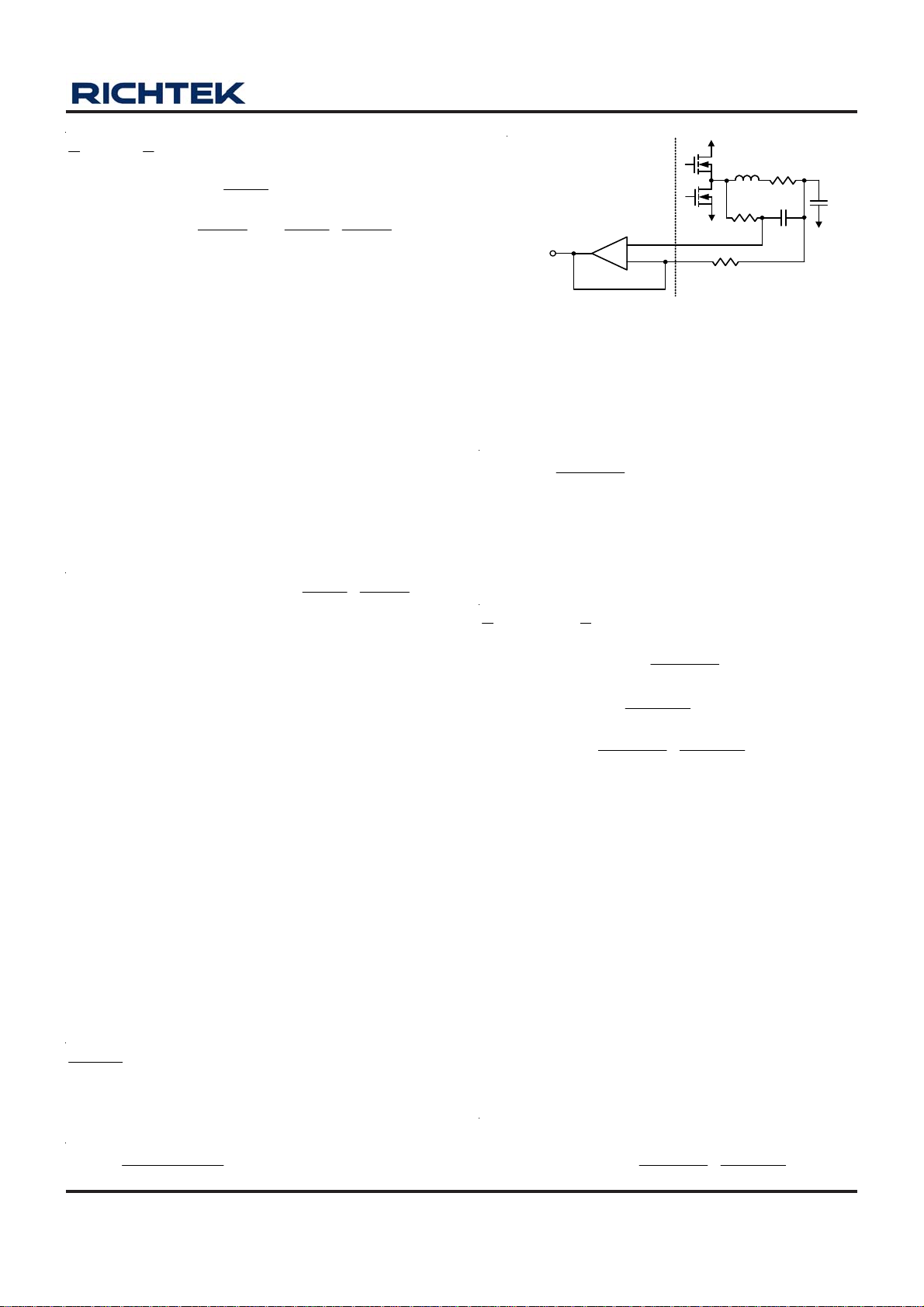
RT8855
11
×=×
II
IMAX X(MAX)
48
V
I2I2
X(MAX) IMAX
II 2
LX(MAX) X(MAX)
Once I
=× =×
=× =××
is larger than 2 x I
X
IMAX
R
IMAX
RR
CSNX CSNX
DCR R DCR
XIMAXX
V
IMAX
, OCP of CORE section is
IMAX
CSA: Current Sense Am plifier
I
X_NB
+
-
triggered and latched. Then, R T8855 will turn off both high
side MOSFET and low side MOSFET of all channels. A
Figure 12. Current Sensing Circuit for NB Section
100us delay is used in OCP detection circuit to prevent
false trigger.
Except the normal OCP function described above, there
is another short-circuit-OCP function especi ally designed
for short circuit protection. Since short circuit may cause
catastrophic da mage over a very short period, this shortcircuit-OCP should have a very short delay for triggering
OCP latch. Also to prevent false trigger, the trigger level
of short-circuit-OCP is designed 1.5 times of normal OCP
level. Hence, the equation of short-circuit-OCP is :
I = 1.5 x I = 3
LX(MAX), short LX(MAX)
V
IMAX
××
R DCR
R
CSNX
IMAX X
,
and the delay of short-curcuit-OCP is 20us. when shortcircuit-OCP is triggered, the RT8855 will turn off both high
side MOSFET and low side MOSFET of all cha nnels.
CORE Section- Over Voltage Protection (OVP)
The over voltage protection monitors the output voltage
via the FB pin. Once V
exceeds 1.8V , OVP is triggered
FB
and latched for VCORE section. RT8855 will try to turn
on each low side MOSFET and turn off each high side
MOSFET to protect CPU.
NB Section- Over Current Protection (OCP)
NB section uses an external resistor R
to IMAX_NB pin to generate a reference current I
for over current protection a s depicted in Figure 13.
V
I
IMAX_NB
where V
the sensed phase current I
IMAX_NB
=
R
IMAX_NB
is typical 1.6V . OCP comparator compares
IMAX_NB
with the reference current.
X_NB
Equivalently , the maxi mum phase NB current I
is calculated as below :
11
×=×
II
IMAX_NB X_NB
48
V
=× =×
I2I 2
X_NB IMAX_NB
II
LX_NB(MAX) X_NB
2
Once I
=×
VR
=× ×
RDCR
is larger than 2 x I
X_NB
IMAX_NB CSN_NB
IMAX_NB NB
R
R
CSN_NB
DCR
IMAX_NB
IMAX_NB
NB
IMAX_NB
is triggered and latched. Then, RT8855 will turn of f both
high side MOSFET and low side MOSFET of NB section.
A 100us delay is used in OCP detection circuit to prevent
NB Section- Output Current Sensing
The RT8855 provides low input offset current-sense
a mplifier (CSA) to monitor the continuous output current
of NB scetion. Output current of CSA (I
) is used for
X_NB
over current detection as shown in Figure 12. In this
inductor current sensing topology , R
S_NB
and C
S_NB
must
be set according to the equation below :
L
NB
DCR
RC
=×
NB
S_NB S_NB
Then the output current of CSA will follow the equation
below :
I DCR
×
I
X_NB
DS8855-00 July 2008 www.richtek.com
L_NB NB
=
R
CSN_NB
false trigger.
Except the normal OCP function described above, there
is another short-circuit-OCP function especi ally designed
for short circuit protection. Since short circuit may cause
catastrophic da mage over a very short period, this shortcircuit-OCP should have a very short delay for triggering
OCP latch. Also to prevent false trigger, the trigger level
of short-circuit-OCP is designed 1.5 times of normal OCP
level of NB section. Hence, the equation of NB section
short-circuit-OCP is :
I = 1.5 x I
LX_NB(MAX), short LX_NB(MAX)
VR
= 3
IMAX_NB CSN_NB
××
RDCR
IMAX_NB
L
NB
DCR
NB
C
S_NB
R
S_NB
R
CSN_NB
IMAX_NB
connected
MAX_NB
LX_NB(MAX)
, OCP of NB se ction
,
NB
15
Page 16
RT8855
and the delay of short-curcuit-OCP of NB section is 20us.
When short-circuit-OCP is triggered at NB section, the
RT8855 will turn off both high side MOSFET a nd low side
MOSFET of NB section.
V
IN
OCP Comparator
1.6V
HS
PWM
Controlle r
LS
+
-
I
IMAX_NB
V
IMAX_NB
R
IMAX_NB
1/8I
X_NB
84
RT8855 NB section
GM
I
X_NB
+
-
1/4I
IMAX_N B
+
-
L
R
X_NB
R
X_NB
CSN_NB
I
LX
DCR
C
NB
X_NB
Figure 13. Over Current Protection for NB section.
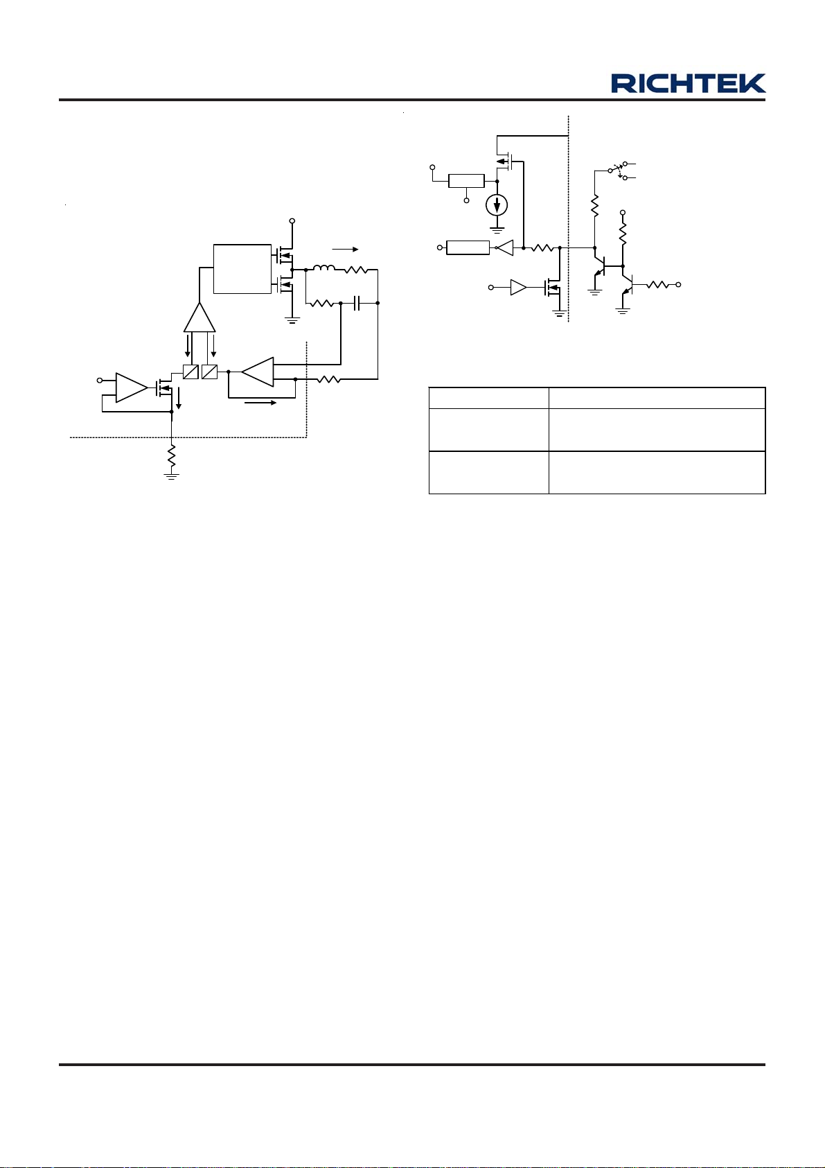
PSOC2P
Latch
EN
Control
PSIA
PSI
(From I2C)
PS pin PSI Strategy
Pull-Up to 3.3V
Pull-Up to 5V
5VCC
(1) 5VCC for (4 phase to 2 phase)
(2) 3.3V for (4 phase to 1 phase)
VDDIO
PS
(Active Low)
Figure 14. Power-Saving-Mode Circuit.
Table 5. PSI Strategy
Phase number is set to 1 while
PSI is asserted.
Phase number is set to 2 while
PSI is asserted.
PSI
NB Section- Over Voltage Protection (OVP)
The over voltage protection monitors the output voltage
via the FB_NB pin. Once V
exceeds 1.8V, OVP is
FB_NB
triggered and latched for NB section. RT8855 will try to
turn on low side MOSFET and turn of f high side MOSFET
to protect NB.
Power Saving Indicator (PSI)
This is an active-low flag that can be set by the CPU to
allow the regulator to enter Power-Saving mode to
maximize the system efficiency when in light-load
conditions. The status of the flag is communicated to the
controller through either the SVI bus or PS pin. RT8855
monitors the PS pin to define the PSI strategy that is the
action perf ormed by the controller when PSI is a sserted.
According Figure 14, by programming dif ferent voltage on
PS pin, it configures the controller to operate in one or
two phases condition when PSI is asserted. Pulling-up
PS pin to 3.3V through a resistor, the controller operates
in only 1 phase configuration. If the 3.3V is changed to
5V , RT8855 operates in 2 pha se configuration. When PSI
is de-asserted, the controller will return to the original
configuration. The PSI strategy is summarized a s shown
in Table 5.
PCB Layout Guideline
Careful PCB layout is critical to achieve low switching
losses and clean, stable operation. The high-power
switching power stage requires particular attention. Follow
these guidelines for optimum PCB layout.
Place the power components first, that includes power
MOSFETs, input and output capa citors, a nd inductors. It
is important to have a symmetrical layout f or ea ch power
train, preferably with the controller located equidistant from
each. Symmetrical layout allows heat to be dissipated
equally across all power trains. Great attention should be
paid for routing the UGATE, LGA TE, and PHASE traces
since they drive the power train MOSFETs using short,
high current pulses. It is important to size them as large
and a s short a s possible to reduce their overall impedance
and inducta nce. Extra care should be given to the LGA TE
traces in particular since keeping their impedance and
inductance low helps to significa ntly reduce the possibility
of shoot-through.
When placing the MOSFETs try to keep the source of the
upper MOSFETs and the drain of the lower MOSFETs
and as close as possible. Input Bulk capacitors should
be placed close to the drain of the upper MOSFETs and
and the source of the lower MOSFETs and .
16
DS8855-00 July 2008www.richtek.com
Page 17

Locate the output inductors and output ca pacitors between
the MOSFET s a nd the load. Route high-speed switching
nodes away from sensitive analog areas (ISP, ISN, FB,
FBRT N, COMP, ADJ, OFS, IMAX.....)
Keep the routing of the bootstra p ca pacitor short between
BOOT and PHASE.
Place the snubber R&C a s close a s possible to the lower
MOSFET s of ea ch pha se.
RT8855
DS8855-00 July 2008 www.richtek.com
17
Page 18
RT8855
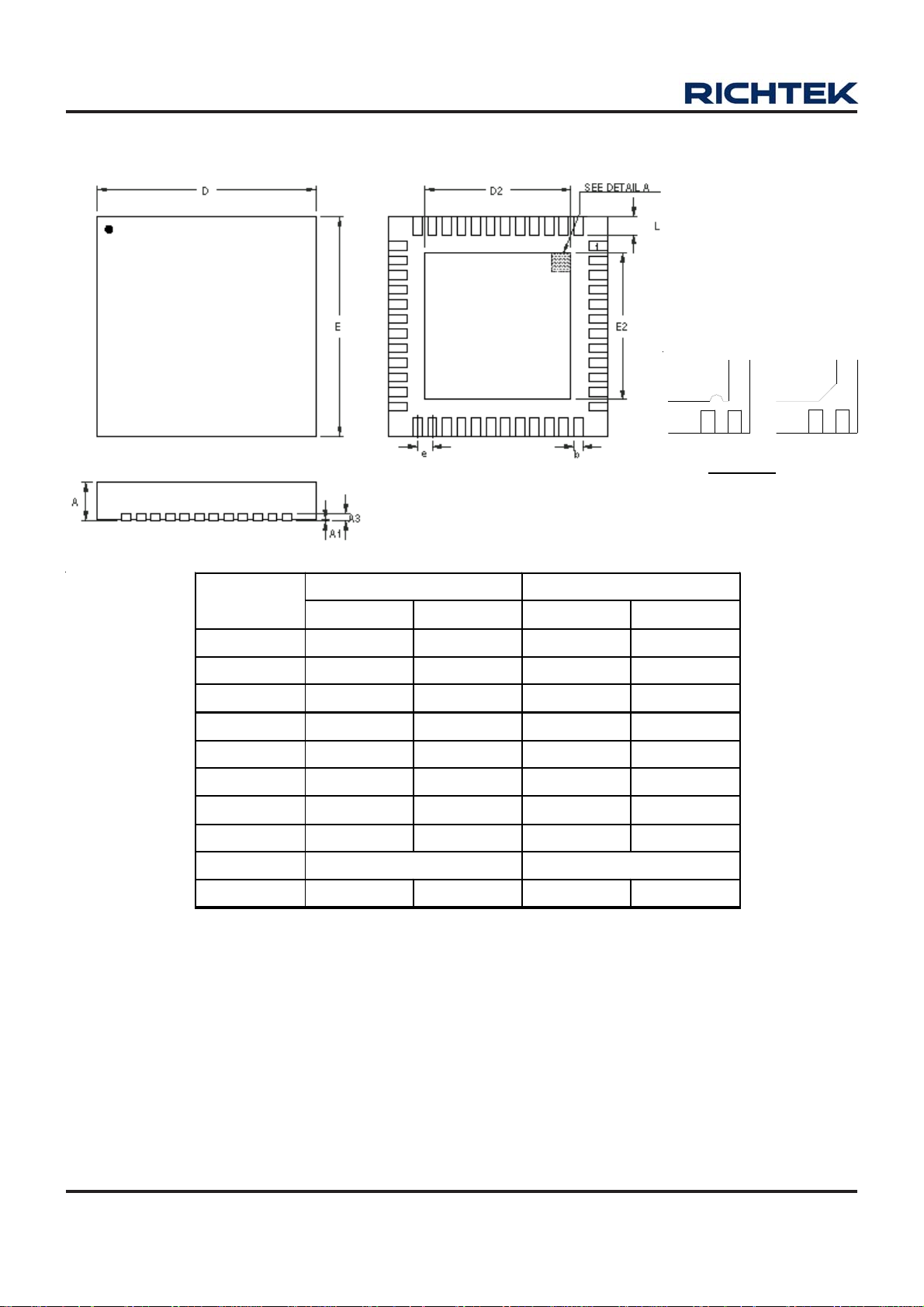
Outline Dimension
2
DETAIL A
Pin #1 ID a nd T ie Bar Mark Option s
Note : The configuration of the Pin #1 identifier is optional,
but must be located within the zone indicated.
Dimensions In Millimeters Dimensions In Inc hes
Symbol
Min Max Min Max
A 0.700 0.800 0.028 0.031
A1 0.000 0.050 0.000 0.002
A3 0.175 0.250 0.007 0.010
b 0.200 0.300 0.008 0.012
D 6.950 7.050 0.274 0.278
D2 5.050 5.250 0.199 0.207
E 6.950 7.050 0.274 0.278
E2 5.050 5.250 0.199 0.207
e 0.500 0.020
1
1
2
L 0.350 0.450
Richtek Technology Corporation
Headquarter
5F, No. 20, Taiyuen Street, Chupei City
Hsinchu, Taiwan, R.O.C.
Tel: (8863)5526789 Fax: (8863)5526611
Information that is provided by Richtek Technology Corporation is believed to be accurate and reliable. Richtek reserves the right to make any change in circuit
design, specification or other related things if necessary without notice at any time. No third party intellectual property infringement of the applications should be
guaranteed by users when integrating Richtek products into any application. No legal responsibility for any said applications is assumed by Richtek.
18
W-Type 48L QFN 7x7 Package
Richtek Technology Corporation
Taipei Office (Marketing)
8F, No. 137, Lane 235, Paochiao Road, Hsintien City
Taipei County, Taiwan, R.O.C.
Tel: (8862)89191466 Fax: (8862)89191465
Email: [email protected]
0.014 0.018
DS8855-00 July 2008www.richtek.com
 Loading...