

Page 1
Conceptual
RT8841
4/3/2/1-Phase PWM Controller for High-Density Power Supply
General Description
The RT8841 is a 4/3/2/1-phase synchronous buck
controller with 2 integrated MOSFET drivers for V R11 CPU
power application. R T8841 uses differential inductor DCR
current sense to achieve pha se current balance a nd active
voltage positioning. Other features include adjustable
operating frequency, adjustable soft start, power good
indication, external error-a mp compensation, over voltage
protection, over current protection and ena ble/shutdown
for various a pplications. RT8841 comes to a small footprint
with WQFN-40L 6x6 pa ckage
Applications
z Desktop CPU Core Power
z Low V oltage, High Current DC/ DC Converter
Ordering Information
RT8841
Package Type
QW : WQFN-40L 6x6 (W-Type)
Operating Temperature Range
P : Pb Free with Commercial Standard
G : Green (Halogen Free with Commer cial Standard)
Note :
Richtek Pb-free and Green products are :
RoHS compliant and compatible with the current require-
`
ments of IPC/JEDEC J-STD-020.
`
Suitable for use in SnPb or Pb-free soldering processes.
100% matte tin (Sn) plating.
`
Features
zz
z
12V Power Supply Voltage
zz
zz
z
4/3/2/1-Phase Power Conversion
zz
zz
z
2 Embedded MOSFET Drivers
zz
zz
z
Internal Regulated 5V Output
zz
zz
z
VID Tables for Intel VRD11/VRD10.x and AMD K8,
zz
K8_M2 CPUs
zz
z
Continuous Differential Inductor DCR Current Sense
zz
zz
z
Adjustable Soft Start
zz
zz
z
Adjustable Frequency
zz
zz
z
Power Good Indication
zz
zz
z Adjustable Over Current Protection
zz
zz
z Over Voltage Protection
zz
zz
z Small 40-Lead WQFN Package
zz
zz
z RoHS Compliant and 100% Lead(Pb)-Free
zz
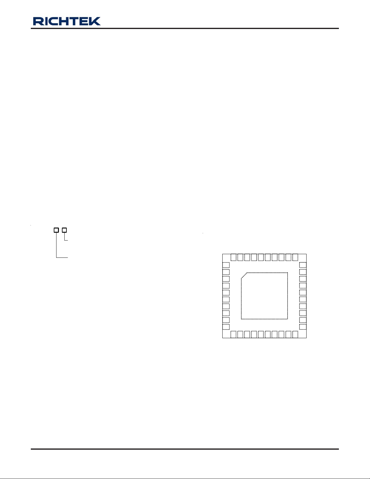
Pin Configurations
(TOP VIEW)
VIDSEL
FBRTN
SS/EN
ADJ
COMP
FB
OFS
RT
IMAX
GND
1
D
I
V
VID0
1
2
3
4
5
6
7
8
9
10
ISP4
ISN4
4
D
I
VID2
VID3
VID5
VID6
VID7
EN/VTT
V
GND
3
N
S
ISP3
ISP2
ISN2
I
ISN1
PWRGD
31323334353637383940
30
BOOT1
29
UGATE1
28
PHASE1
27
LGATE1
26
VCC12
25
LGATE2
24
PHASE2
23
20191817161514131211
VCC5
22
21
PWM4
UGATE2
BOOT2
PWM3
41
ISP1
WQFN-40L 6x6
DS8841-02C September 2007 www.richtek.com
1
Page 2
RT8841
O
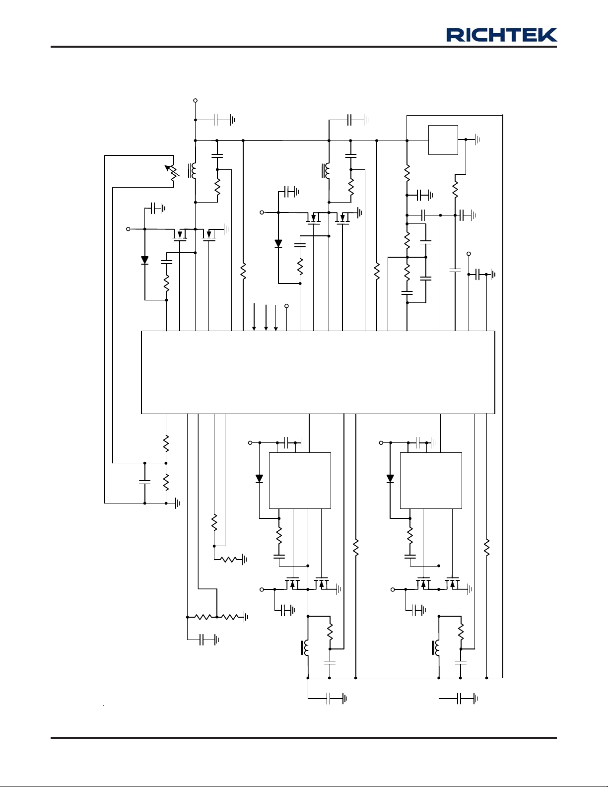
Typical Application Circuit
C
V
C
1
T
L
N
V
2
1
7
8
9
0
3
1
T
O
O
B
1
4
8
8
T
R
J
D
A
4
2
2
2
1
E
T
A
G
U
1
1
E
E
T
S
A
A
G
H
L
P
5
C
S
F
T
C
O
R
V
7
8
9
1
Conceptual
LOAD
2
L
V
2
1
V
2
1
0
4
o
t
3
8
3
1
1
1
1
P
N
S
S
I
I
X
A
M
I
9
V
2
1
1
1
3
3
]
0
:
7
[
D
I
V
D
T
L
T
E
G
V
S
R
/
D
N
I
W
E
V
P
2
7
4
3
2
2
2
2
2
2
2
T
E
E
T
S
O
A
A
O
H
G
B
P
U
3
M
W
P
1
2
5
5
2
2
E
T
A
G
L
4
1
6
1
1
2
P
S
I
3
3
P
N
S
S
I
I
3
1
5
6
2
B
P
F
N
M
S
I
O
C
V
2
1
2
3
N
T
R
B
F
4
M
W
P
0
2
0
6
1
2
2
N
E
/
S
S
D
1
N
C
G
C
V
4
4
P
N
S
S
I
I
2
1
1
1
VCC
GND
BOOT
UGATE
V
2
1
2
L
PWM
PHASE
LGATE
9
1
6
9
T
R
VCC
GND
BOOT
UGATE
V
2
1
2
L
PWM
PHASE
LGATE
9
1
6
9
T
R
DS8841-02C September 2007www.richtek.com
2
Page 3

Conceptual
Table 1. Output Voltage Program (VRD10.x + VID6)
RT8841
Pin Name
VID4 VID3 VID2 VID1 VID0 VID5 VID6
0 1 0 1 0 1 1 1.60000V
0 1 0 1 0 1 0 1.59375V
0 1 0 1 1 0 1 1.58750V
0 1 0 1 1 0 0 1.58125V
0 1 0 1 1 1 1 1.57500V
0 1 0 1 1 1 0 1.56875V
0 1 1 0 0 0 1 1.56250V
0 1 1 0 0 0 0 1.55625V
0 1 1 0 0 1 1 1.55000V
0 1 1 0 0 1 0 1.54375V
0 1 1 0 1 0 1 1.53750V
0 1 1 0 1 0 0 1.53125V
0 1 1 0 1 1 1 1.52500V
0 1 1 0 1 1 0 1.51875V
0 1 1 1 0 0 1 1.51250V
0 1 1 1 0 0 0 1.50625V
0 1 1 1 0 1 1 1.50000V
0 1 1 1 0 1 0 1.49375V
0 1 1 1 1 0 1 1.48750V
0 1 1 1 1 0 0 1.48125V
0 1 1 1 1 1 1 1.47500V
0 1 1 1 1 1 0 1.46875V
1 0 0 0 0 0 1 1.46250V
1 0 0 0 0 0 0 1.45625V
1 0 0 0 0 1 1 1.45000V
1 0 0 0 0 1 0 1.44375V
1 0 0 0 1 0 1 1.43750V
1 0 0 0 1 0 0 1.43125V
1 0 0 0 1 1 1 1.42500V
1 0 0 0 1 1 0 1.41875V
1 0 0 1 0 0 1 1.41250V
1 0 0 1 0 0 0 1.40625V
1 0 0 1 0 1 1 1.40000V
1 0 0 1 0 1 0 1.39375V
1 0 0 1 1 0 1 1.38750V
1 0 0 1 1 0 0 1.38125V
1 0 0 1 1 1 1 1.37500V
1 0 0 1 1 1 0 1.36875V
1 0 1 0 0 0 1 1.36250V
Nominal Output Voltage DACOUT
DS8841-02C September 2007 www.richtek.com
To be continued
3
Page 4

RT8841
Conceptual
Table 1. Output Voltage Program (VRD10.x + VID6)
Pin Name
VID4 VID3 VID2 VID1 VID0 VID5 VID6
1 0 1 0 0 0 0 1.35625V
1 0 1 0 0 1 1 1.35000V
1 0 1 0 0 1 0 1.34375V
1 0 1 0 1 0 1 1.33750V
1 0 1 0 1 0 0 1.33125V
1 0 1 0 1 1 1 1.32500V
1 0 1 0 1 1 0 1.31875V
1 0 1 1 0 0 1 1.31250V
1 0 1 1 0 0 0 1.30625V
1 0 1 1 0 1 1 1.30000V
1 0 1 1 0 1 0 1.29375V
1 0 1 1 1 0 1 1.28750V
1 0 1 1 1 0 0 1.28125V
1 0 1 1 1 1 1 1.27500V
1 0 1 1 1 1 0 1.26875V
1 1 0 0 0 0 1 1.26250V
1 1 0 0 0 0 0 1.25625V
1 1 0 0 0 1 1 1.25000V
1 1 0 0 0 1 0 1.24375V
1 1 0 0 1 0 1 1.23750V
1 1 0 0 1 0 0 1.23125V
1 1 0 0 1 1 1 1.22500V
1 1 0 0 1 1 0 1.21875V
1 1 0 1 0 0 1 1.21250V
1 1 0 1 0 0 0 1.20625V
1 1 0 1 0 1 1 1.20000V
1 1 0 1 0 1 0 1.19375V
1 1 0 1 1 0 1 1.18750V
1 1 0 1 1 0 0 1.18125V
1 1 0 1 1 1 1 1.17500V
1 1 0 1 1 1 0 1.16875V
1 1 1 0 0 0 1 1.16250V
1 1 1 0 0 0 0 1,15625V
1 1 1 0 0 1 1 1.15000V
1 1 1 0 0 1 0 1.14375V
1 1 1 0 1 0 1 1.13750V
1 1 1 0 1 0 0 1.13125V
1 1 1 0 1 1 1 1.12500V
1 1 1 0 1 1 0 1.11875V
Nominal Output Voltage DACOUT
To be continued
DS8841-02C September 2007www.richtek.com
4
Page 5

Conceptual
Table 1. Output Voltage Program (VRD10.x + VID6)
RT8841
Pin Name
VID4 VID3 VID2 VID1 VID0 VID5 VID6
1 1 1 1 0 0 1 1.11250V
1 1 1 1 0 0 0 1.10625V
1 1 1 1 0 1 1 1.10000V
1 1 1 1 0 1 0 1.09375V
1 1 1 1 1 0 1 OFF
1 1 1 1 1 0 0 OFF
1 1 1 1 1 1 1 OFF
1 1 1 1 1 1 0 OFF
0 0 0 0 0 0 1 1.08750V
0 0 0 0 0 0 0 1.08125V
0 0 0 0 0 1 1 1.07500V
0 0 0 0 0 1 0 1.06875V
0 0 0 0 1 0 1 1.06250V
0 0 0 0 1 0 0 1.05625V
0 0 0 0 1 1 1 1.05000V
0 0 0 0 1 1 0 1.04375V
0 0 0 1 0 0 1 1.03750V
0 0 0 1 0 0 0 1.03125V
0 0 0 1 0 1 1 1.02500V
0 0 0 1 0 1 0 1.01875V
0 0 0 1 1 0 1 1.01250V
0 0 0 1 1 0 0 1.00625V
0 0 0 1 1 1 1 1.00000V
0 0 0 1 1 1 0 0.99375V
0 0 1 0 0 0 1 0.98750V
0 0 1 0 0 0 0 0.98125V
0 0 1 0 0 1 1 0.97500V
0 0 1 0 0 1 0 0.96875V
0 0 1 0 1 0 1 0.96250V
0 0 1 0 1 0 0 0.95625V
0 0 1 0 1 1 1 0.95000V
0 0 1 0 1 1 0 0.94375V
0 0 1 1 0 0 1 0.93750V
0 0 1 1 0 0 0 0.93125V
0 0 1 1 0 1 1 0.92500V
0 0 1 1 0 1 0 0.91875V
0 0 1 1 1 0 1 0.91250V
0 0 1 1 1 0 0 0.90625V
0 0 1 1 1 1 1 0.90000V
Nominal Output Voltage DACOUT
DS8841-02C September 2007 www.richtek.com
To be continued
5
Page 6

RT8841
Conceptual
Table 1. Output Voltage Program (VRD10.x + VID6)
Pin Name
VID4 VID3 VID2 VID1 VID0 VID5 VID6
0 0 1 1 1 1 0 0.89375V
0 1 0 0 0 0 1 0.88750V
0 1 0 0 0 0 0 0.88125V
0 1 0 0 0 1 1 0.87500V
0 1 0 0 0 1 0 0.86875V
0 1 0 0 1 0 1 0.86250V
0 1 0 0 1 0 0 0.85625V
0 1 0 0 1 1 1 0.85000V
0 1 0 0 1 1 0 0.84375V
0 1 0 1 0 0 1 0.83750V
0 1 0 1 0 0 0 0.83125V
Nominal Output Voltage DACOUT
DS8841-02C September 2007www.richtek.com
6
Page 7

Conceptual
Table 2. Output Voltage Program (VRD11)
RT8841
Pin Name
HEX
00 OFF
01 OFF
02 1.60000V
03 1.59375V
04 1.58750V
05 1.58125V
06 1.57500V
07 1.56875V
08 1.56250V
09 1.55625V
0A 1.55000V
0B 1.54375V
0C 1.53750V
0D 1.53125V
0E 1.52500V
0F 1.51875V
10 1.51250V
11 1.50625V
12 1.50000V
13 1.49375V
14 1.48750V
15 1.48125V
16 1.47500V
17 1.46875V
18 1.46250V
19 1.45625V
1A 1.45000V
1B 1.44375V
1C 1.43750V
1D 1.43125V
1E 1.42500V
1F 1.41875V
20 1.41250V
21 1.40625V
22 1.40000V
23 1.39375V
24 1.38750V
25 1.38125V
26 1.37500V
Nominal Output Voltage
DACOUT
Pin Name
Nominal Output Voltage DACOUT
HEX
27 1.36875V
28 1.36250V
29 1.35625V
2A 1.35000V
2B 1.34375V
2C 1.33750V
2D 1.33125V
2E 1.32500V
2F 1.31875V
30 1.31250V
31 1.30625V
32 1.30000V
33 1.29375V
34 1.28750V
35 1.28125V
36 1.27500V
37 1.26875V
38 1.26250V
39 1.25625V
3A 1.25000V
3B 1.24375V
3C 1.23750V
3D 1.23125V
3E 1.22500V
3F 1.21875V
40 1.21250V
41 1.20625V
42 1.20000V
43 1.19375V
44 1.18750V
45 1.18125V
46 1.17500V
47 1.16875V
48 1.16250V
49 1.15625V
4A 1.15000V
4B 1.14375V
4C 1.13750V
4D 1.13125V
To be continued
DS8841-02C September 2007 www.richtek.com
7
Page 8

RT8841
Conceptual
Table 2. Output Voltage Program (VRD11)
Pin Name
Nominal Output Voltage DACOUT
HEX
4E 1.12500V
4F 1.11875V
50 1.11250V
51 1.10625V
52 1.10000V
53 1.09375V
54 1.08750V
55 1.08125V
56 1.07500V
57 1.06875V
58 1.06250V
59 1.05625V
5A 1.05000V
5B 1.04375V
5C 1.03750V
5D 1.03125V
5E 1.02500V
5F 1.01875V
60 1.01250V
61 1.00625V
62 1.00000V
63 0.99375V
64 0.98750V
65 0.98125V
66 0.97500V
67 0.96875V
68 0.96250V
69 0.95625V
6A 0.95000V
6B 0.94375V
6C 0.93750V
6D 0.93125V
6E 0.92500V
6F 0.91875V
70 0.91250V
71 0.90625V
72 0.90000V
73 0.89375V
74 0.88750V
Pin Name
Nominal Output Voltage DACOUT
HEX
75 0.88125V
76 0.87500V
77 0.86875V
78 0.86250V
79 0.85625V
7A 0.85000V
7B 0.84375V
7C 0.83750V
7D 0.83125V
7E 0.82500V
7F 0.81875V
80 0.81250V
81 0.80625V
82 0.80000V
83 0.79375V
84 0.78750V
85 0.78125V
86 0.77500V
87 0.76875V
88 0.76250V
89 0.75625V
8A 0.75000V
8B 0.74375V
8C 0.73750V
8D 0.73125V
8E 0.72500V
8F 0.71875V
90 0.71250V
91 0.70625V
92 0.70000V
93 0.69375V
94 0.68750V
95 0.68125V
96 0.67500V
97 0.66875V
98 0.66250V
99 0.65625V
9A 0.65000V
9B 0.64375V
To be continued
DS8841-02C September 2007www.richtek.com
8
Page 9

Conceptual
Table 2. Output Voltage Program (VRD11)
RT8841
Pin Name
Nominal Output Voltage DACOUT
HEX
9C 0.63750V
9D 0.63125V
9E 0.62500V
9F 0.61875V
A0 0.61250V
A1 0.60625V
A2 0.60000V
A3 0.59375V
A4 0.58750V
A5 0.58125V
A6 0.57500V
A7 0.56875V
A8 0.56250V
A9 0.55625V
AA 0.55000V
AB 0.54375V
AC 0.53750V
AD 0.53125V
AE 0.52500V
AF 0.51875V
B0 0.51250V
B1 0.50625V
B2 0.50000V
B3 X
B4 X
B5 X
B6 X
B7 X
B8 X
B9 X
BA X
BB X
BC X
BD X
BE X
BF X
C0 X
C1 X
C2 X
Pin Name
Nominal Output Voltage DACOUT
HEX
C3 X
C4 X
C5 X
C6 X
C7 X
C8 X
C9 X
CA X
CB X
CC X
CD X
CE X
CF X
D0 X
D1 X
D2 X
D3 X
D4 X
D5 X
D6 X
D7 X
D8 X
D9 X
DA X
DB X
DC X
DD X
DE X
DF X
E0 X
E1 X
E2 X
E3 X
E4 X
E5 X
E6 X
E7 X
E8 X
E9 X
To be continued
DS8841-02C September 2007 www.richtek.com
9
Page 10

RT8841
Conceptual
Table 2. Output Voltage Program (VRD11)
Pin Name
HEX
EA X
EB X
EC X
ED X
EE X
EF X
F0 X
F1 X
F2 X
F3 X
F4 X
F5 X
F6 X
F7 X
F8 X
F9 X
FA X
FB X
FC X
FD X
FE OFF
FF OFF
Nominal Output Voltage DACOUT
Note: (1) 0 : Connected to GND
(2) 1 : Open
(3) X : Don
10
't Care
DS8841-02C September 2007www.richtek.com
Page 11

Conceptual
Table 3. Output Voltage Program (K8)
VID4 VID3 VID2 VID1 VID0 Nominal Output Voltage DACOUT
0 0 0 0 0 1.550
0 0 0 0 1 1.525
0 0 0 1 0 1.500
0 0 0 1 1 1.475
0 0 1 0 0 1.450
0 0 1 0 1 1.425
0 0 1 1 0 1.400
0 0 1 1 1 1.375
0 1 0 0 0 1.350
0 1 0 0 1 1.325
0 1 0 1 0 1.200
0 1 0 1 1 1.275
0 1 1 0 0 1.250
RT8841
0 1 1 0 1 1.225
0 1 1 1 0 1.200
0 1 1 1 1 1.175
1 0 0 0 0 1.150
1 0 0 0 1 1.125
1 0 0 1 0 1.100
1 0 0 1 1 1.075
1 0 1 0 0 1.050
1 0 1 0 1 1.025
1 0 1 1 0 1.000
1 0 1 1 1 0.975
1 1 0 0 0 0.950
1 1 0 0 1 0.925
1 1 0 1 0 0.900
1 1 0 1 1 0.875
1 1 1 0 0 0.850
1 1 1 0 1 0.825
1 1 1 1 0 0.800
1 1 1 1 1 Shutdown
Note: (1) 0 : Connected to GND
(2) 1 : Open
DS8841-02C September 2007 www.richtek.com
11
Page 12

RT8841
Conceptual
Table 4. Output Voltage Program (K8_M2)
Pin Name
VID5 VID4 VID3 VID2 VID1 VID0
0 0 0 0 0 0 1.5500
0 0 0 0 0 1 1.5250
0 0 0 0 1 0 1.5000
0 0 0 0 1 1 1.4750
0 0 0 1 0 0 1.4500
0 0 0 1 0 1 1.4250
0 0 0 1 1 0 1.4000
0 0 0 1 1 1 1.3750
0 0 1 0 0 0 1.3500
0 0 1 0 0 1 1.3250
0 0 1 0 1 0 1.3000
0 0 1 0 1 1 1.2750
0 0 1 1 0 0 1.2500
0 0 1 1 0 1 1.2250
0 0 1 1 1 0 1.2000
Nominal Output Voltage DACOUT
0 0 1 1 1 1 1.1750
0 1 0 0 0 0 1.1500
0 1 0 0 0 1 1.1250
0 1 0 0 1 0 1.1000
0 1 0 0 1 1 1.0750
0 1 0 1 0 0 1.0500
0 1 0 1 0 1 1.0250
0 1 0 1 1 0 1.0000
0 1 0 1 1 1 0.9750
0 1 1 0 0 0 0.9500
0 1 1 0 0 1 0.9250
0 1 1 0 1 0 0.9000
0 1 1 0 1 1 0.8750
0 1 1 1 0 0 0.8500
0 1 1 1 0 1 0.8250
0 1 1 1 1 0 0.8000
0 1 1 1 1 1 0.7750
1 0 0 0 0 0 0.7625
1 0 0 0 0 1 0.7500
DS8841-02C September 2007www.richtek.com
12
To be continued
Page 13

Conceptual
Table 4. Output Voltage Program (K8_M2)
RT8841
Pin Name
VID5 VID4 VID3 VID2 VID1 VID0
1 0 0 0 1 0 0.7375
1 0 0 0 1 1 0.7250
1 0 0 1 0 0 0.7125
1 0 0 1 0 1 0.7000
1 0 0 1 1 0 0.6875
1 0 0 1 1 1 0.6750
1 0 1 0 0 0 0.6625
1 0 1 0 0 1 0.6500
1 0 1 0 1 0 0.6375
1 0 1 0 1 1 0.6250
1 0 1 1 0 0 0.6125
1 0 1 1 0 1 0.6000
1 0 1 1 1 0 0.5875
1 0 1 1 1 1 0.5750
1 1 0 0 0 0 0.5625
Nominal Output Voltage DACOUT
1 1 0 0 0 1 0.5500
1 1 0 0 1 0 0.5375
1 1 0 0 1 1 0.5250
1 1 0 1 0 0 0.5125
1 1 0 1 0 1 0.5000
1 1 0 1 1 0 0.4875
1 1 0 1 1 1 0.4750
1 1 1 0 0 0 0.4625
1 1 1 0 0 1 0.4500
1 1 1 0 1 0 0.4375
1 1 1 0 1 1 0.4250
1 1 1 1 0 0 0.4125
1 1 1 1 0 1 0.4000
1 1 1 1 1 0 0.3875
1 1 1 1 1 1 0.3750
Note: (1) 0 : Connected to GND
(2) 1 : Open
(3) The voltage above are load independent for desktop and server platforms. For mobile platforms the voltage above
correspond to zero load current.
DS8841-02C September 2007 www.richtek.com
13
Page 14

RT8841
Conceptual
Functional Pin Description
Pin No. Pin Name Pin Function
1 VIDSEL VID DAC Selection Pin.
2 FBRTN Negative remote sense pin of output voltage.
3 SS/EN
4 ADJ Connect this pin to GND by a resistor to set loadline.
5 COMP Output of error-amp and input of PWM comparator.
6 FB Inverting input of error-amp.
7 OFS Connect this pin to GND by a resistor to set no-load offset voltage.
8 RT Connect this pin to GND by a resistor to adjust frequency.
9 IMAX
10 GND Ground Pin
11,14,15,18 ISP4, ISP3, ISP2, ISP1 Positive current sense pin of channel 1, 2, 3 and 4.
12,13,16,17 ISN4, ISN3, ISN2, ISN1 Negative current sense pin of channel 1, 2, 3 and 4.
19 VCC5 Connect this pin to GND by a ceramic cap larger than 1uF.
20,21 PWM4, PWM3 PWM output for channel 4 and channel 3.
22,30 BOOT2, BOOT1 Bootstrap supply for channel 2 and channel 1.
23,29 UGATE2, UGATE1 Upper gate driver for channel 2 and channel 1.
24,28 PHASE2, PHASE1 Switching node of channel 2 and channel 1.
25,27 LGATE2, LGATE1 Lower gate driver for channel 2 and channel 1.
26 VCC12 IC power supply. Connect to 12V.
31 PWRGD Power good indicator.
32 EN/VTT VTT voltage detector input.
33 to 40 VID7 to VID0 Voltage identification input for DAC.
Exposed pad(41) GND
Connect this pin to GND by a capacitor to adjust soft start time.
Pull this pin to GND to disable controller.
Negative input of OCP comparator. (Positive input of OCP
comparator is ADJ).
E xpose d pa d s hou ld be s ol dered to PCB bo ar d an d conn ect ed t o
GND.
VID Table Selection
VIDSEL VID [7] Table
VTT X VR11
GND X VR10.x
VCC5 VTT K8
VCC5 GND K8_M2
14
DS8841-02C September 2007www.richtek.com
Page 15
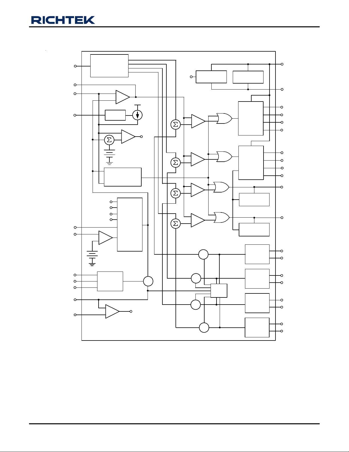
Function Block Diagram
Conceptual
RT8841
RT
COMP
FB
OFS
SS/EN
EN/VTT
VIDOFF
+
Modulator
Waveform
Generator
Offset
+
Transient
Response
Enhancement
OV
OC
POR
+
-
850mV
-
EA
+
+
-
150mV
Soft Start
and
Fault
Logic
OV
POR
+
-
+
-
+
-
+
-
Power-On
Reset
+
-
Regulator
I_SEN1
5V
MOSFET
Driver
MOSFET
Driver
CH3_EN
Detector
CH4_EN
Detector
CH1
Current
SENSE
VCC12
VCC5
BOOT1
UGATE1
PHASE1
LGATE1
BOOT2
UGATE2
PHASE2
LGATE2
PWM3
PWM4
ISP1
ISN1
VIDSEL
VID7 to VID0
FBRTN
ADJ
IMAX
VID
Table
Generator
+
-
OC
+
+
-
-
-
+
-
+
I_SEN2
AVG
I_SEN3
I_SEN4
CH2
Current
SENSE
CH3
Current
SENSE
CH4
Current
SENSE
ISP2
ISN2
ISP3
ISN3
ISP4
ISN4
DS8841-02C September 2007 www.richtek.com
15
Page 16
RT8841
C
Conceptual
Absolute Maximum Ratings (Note 1)
z Supply Input Voltage--------------------------------------------------------------------------------------------------------- −0.3V to 15V
z BOOTx to PHASEx---------------------------------------------------------------------------------------------------------- −0.3V to 15V
z BOOTx to GND---------------------------------------------------------------------------------------------------------------- −0.3V to 30V
z PHASEx to GND-------------------------------------------------------------------------------------------------------------- −2V to 15V
z Input/Output Voltage--------------------------------------------------------------------------------------------------------- −0.3V to 7V
z Power Dissipation, P
D
@ T
= 25°C
A
WQFN−40L 6x6--------------------------------------------------------------------------------------------------------------- 2.778W
z Package Thermal Re sistance (Note 4)
WQF N-40L 6x6, θJA---------------------------------------------------------------------------------------------------------- 36°C/W
z Junction T emperature-------------------------------------------------------------------------------------------------------- 150°C
z Lead T e mperature (Soldering, 10 sec.)---------------------------------------------------------------------------------- 26 0°C
z ESD Susceptibility (Note 2)
HBM (Human Body Mode) ------------------------------------------------------------------------------------------------- 2kV
MM (Ma chine Mode)--------------------------------------------------------------------------------------------------------- 200V
Recommended Operating Conditions (Note 3)
z Supply V oltage, VCC12---------------------------------------------------------------------------------------------------- 12V ± 10%
z Junction T emperature Range---------------------------------------------------------------------------------------------- −40°C to 125°C
z Ambient T emperature Range----------------------------------------------------------------------------------------------
0°C to 70°C
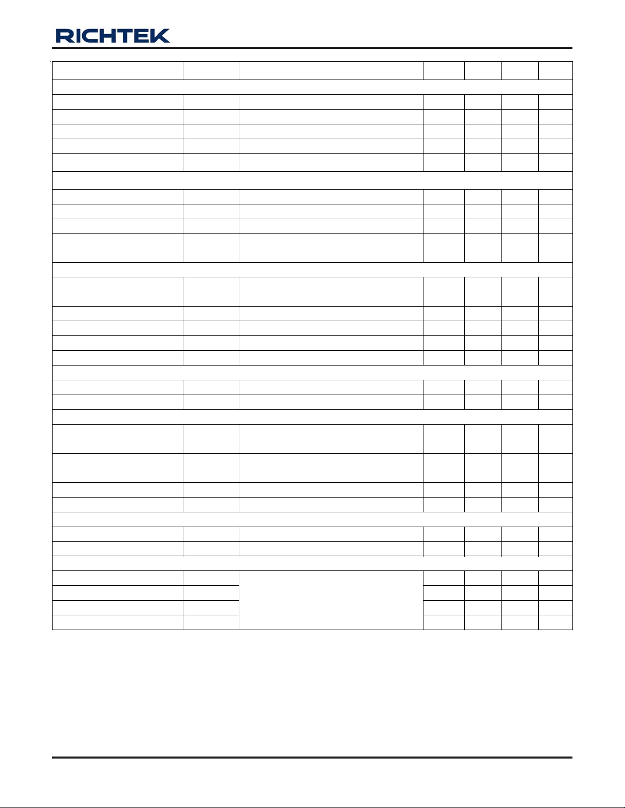
Electrical Characteristics
(VCC12 = 12V, V
Parameter Symbol Conditions Min Typ Max Unit
VCC12 Supply Input
VCC12 Supply Voltage V
VCC12 Supply Current I
V CC5 powe r
V CC 5 Su ppl y Volt ag e V
V CC5 Out put Sour cing I
Power-On Reset
VCC12 Rising Threshold V
VCC12 Hysteresis V
VCC5 Risi ng Thresho ld V
VCC5 Hystere sis V
Power Monitor
Power Monitor Maximum
Output Voltage
EN/VTT
EN/VTT Ri sing Thre shold V
Enable Hysteresis V
Reference Voltage accuracy
DAC Accuracy
= 0V, TA = 25°C, unless otherwise specified)
GND
10.8 12 13.2 V
VCC12
-- 6 -- mA
C
I
VCC5
20 -- -- mA
VCC5
VCC12TH
VCC12HY
VCC5TH
VCC5HY
-- 1.15 -- V
EN/VTT Rising 0.80 0.85 0.90 V
ENVTT
ENVTTHY
= 10mA 4.75 5.0 5.25 V
LOAD
VCC12 Rising 9.2 9.6 10.0 V
VCC12 Falling -- 0.9 -- V
VCC5 Rising 4.4 4.6 4.8 V
VCC5 Falling -- 0.4 -- V
EN/VTT Falling -- 100 -- mV
0.8V to 1.6V −5 -- +5 mV
0.5V to 0.8V −8 -- +8 mV
To be continued
DS8841-02C September 2007www.richtek.com
16
Page 17
Conceptual
RT8841
Parameter Symbol Conditions Min Typ Max Unit
Error Amplifier
DC Gain ADC No Load -- 80 -- dB
Gain-Bandwidth GBW C
Slew Rate SR C
Output voltage range V
Max Current I
0.5 3.6 V
COMP
EA_SLEW
Slew 300 -- -- μA
= 10pF -- 10 -- MHz
LOAD
= 10pF 10 -- -- V/μs
LOAD
Power Sequence
PWRGD Low Voltage V
PGOOD
I
PWRGD
= 4mA -- -- 0.4 V
Soft-Start Delay TD1 -- 2 -- ms
V
PWRGD Delay TD5
Duration TD3 -- 0.8 -- ms
BOOT
Measured the time f orm V
to PWRGD = 1
BOOT
change
-- 1.6 -- ms
Current Sense Amplifier
= 1.3V
V
Max Current I
Input Offset Voltage V
Running Frequency f
GMMAX
−1 0 1 mV
OSCS
R
OSC
RT Pin Voltage VRT R
Ramp Amplitude V
R
RAMP
CSP
Sink Current from CSN
= 40kΩ 280 300 320 kHz
RT
= 40kΩ 1.52 1.60 1.68 V
RT
= 40kΩ -- 1.60 -- V
RT
100 -- -- μA
Soft Start
Soft Start Current I
VID change Current I
Slew 6 8 10 μA
SS1
Slew 60 80 100 μA
SS2
Gate Driver
UGATE Drive Source R
UGATE Drive Sink R
LGATE Drive Source R
LGATE Drive Sink R
UGATEsr
UGATEsk
LGATEsr
LGATEsk
BOOT − PHASE = 8V
250mA Source Current
BOOT − PHASE = 8V
250mA Sink Current
V
= 8V -- 1 -- Ω
LGATE
-- 1 -- Ω
-- 1 -- Ω
250mA Sink Current -- 0.8 -- Ω
Protection
Over-Voltage Threshold V
Over-Current Threshold V
Sweep FB Voltage, V
OVP
Swee p IMAX Voltage, V
OCP
125 150 175 mV
FB,EAP
IMAX,ADJ
−10 0 +10 mV
Dynamic Characteristic
UGATE Rise Time t
UGATE Fall Time t
LGATE Rise Time t
LGATE Fall Time t
rUGATE
fUGATE
rLGATE
fLGATE
-- 15 -- ns
-- 10 -- ns
Ciss = 3000p
-- 15 -- ns
-- 10 -- ns
DS8841-02C September 2007 www.richtek.com
17
Page 18

RT8841
Note 1. Stresses listed as the above “Absolute Maximum Ratings” may cause permanent damage to the device. These are for
stress ratings. Functional operation of the device at these or any other conditions beyond those indicated in the
operational sections of the specifications is not implied. Exposure to absolute maximum rating conditions for extended
periods may remain possibility to affect device reliability.
Note 2. Devices are ESD sensitive. Handling precaution recommended.
Note 3. The device is not guaranteed to function outside its operating conditions.
Note 4. θ
is measured in the natural convection at TA = 25°C on a effective single layer thermal conductivity test board of
JA
JEDEC thermal measurement standard.
Conceptual
18
To be continued
DS8841-02C September 2007www.richtek.com
Page 19
Conceptual
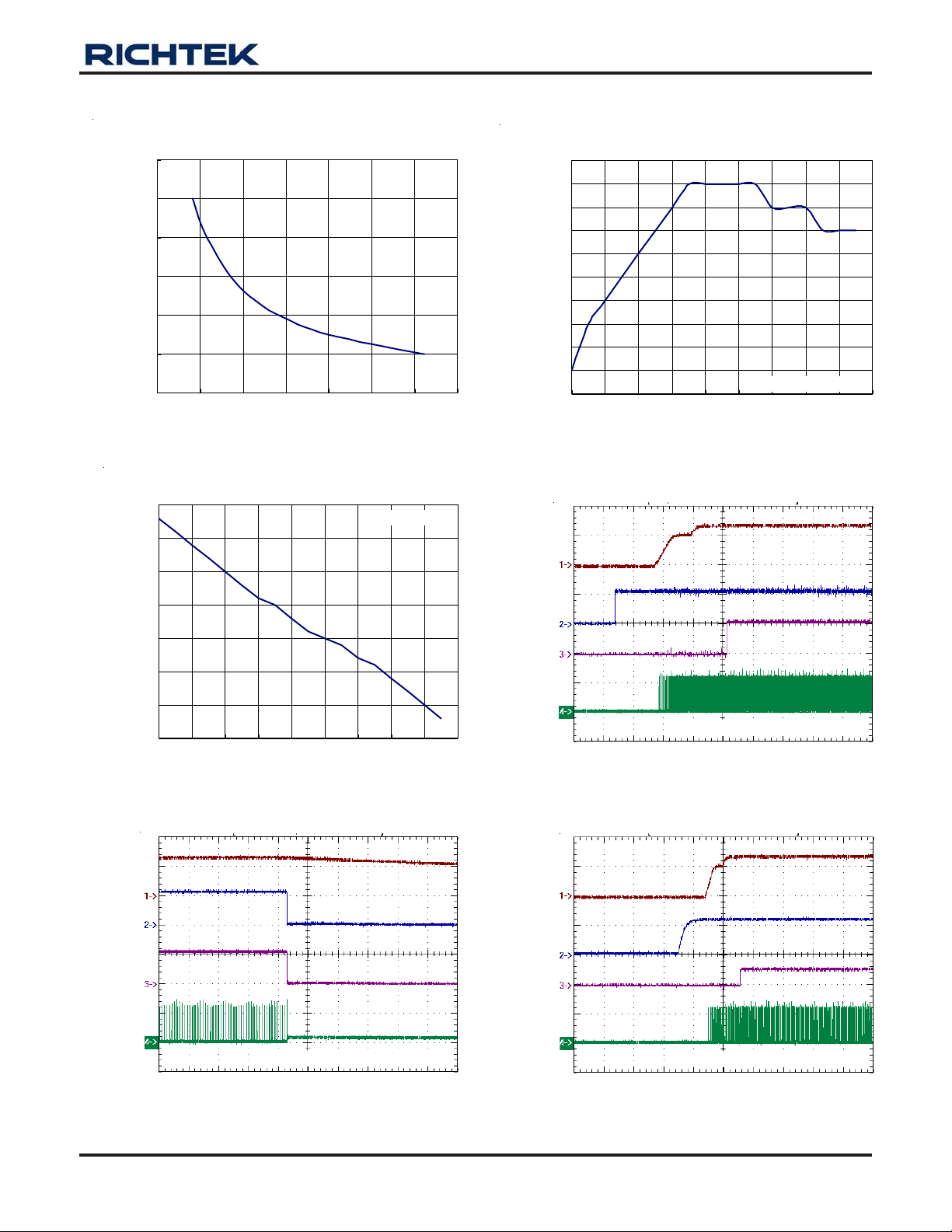
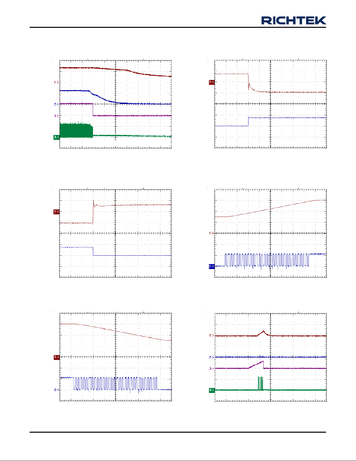
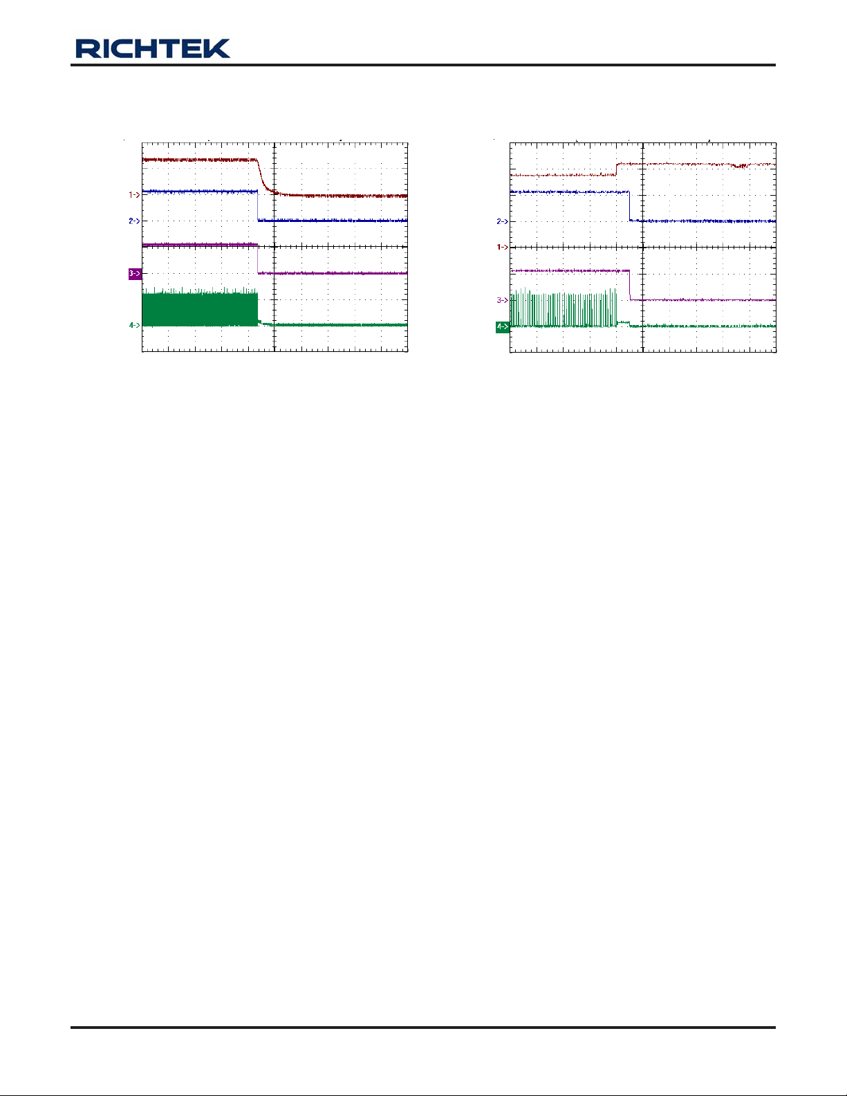
Typical Operating Characteristics
RT8841
Frequency vs. R
1200
1000
800
600
400
RT
Frequency ( kH z)
200
0
0 10203040506070
R
(kΩ)
RT
Frequency vs. Temperature
380
375
370
RRT = 30.1kΩ
1.324
1.323
1.322
1.321
1.320
1.319
1.318
1.317
Output Voltage (V)
1.316
1.315
1.314
V
OUT
(1V/Div)
Output Voltage vs. Temperature
VIN = 12V, I
-40 -20 0 20 40 60 80 100 120 140
Temperature
OUT
= 0A
Power On from VTT/EN
365
360
355
Frequency ( kH z)
350
345
V
OUT
(1V/Div)
VTT/EN
(1V/Div)
SS
(2V/Div)
PHASE
(10V/Div)
-40 -20 0 20 40 60 80 100 120 140
Temperature
(°C)
Power Off from VTT/EN
VIN = 12V, V
= 1.4V, I
OUT
OUT
= 0A
VTT/EN
(1V/Div)
PGOOD
(1V/Div)
PHASE
(10V/Div)
V
OUT
(1V/Div)
V
IN
(10V/Div)
PGOOD
(2V/Div)
PHASE
(10V/Div)
VIN = 12V, V
= 1.4V, I
OUT
Time (2ms/Div)
Power On from VIN
VIN = 12V, V
= 1.4V, I
OUT
OUT
OUT
= 0A
= 0A
Time (40us/Div)
Time (4ms/Div)
DS8841-02C September 2007 www.richtek.com
19
Page 20
RT8841
Conceptual
V
OUT
(1V/Div)
V
IN
(10V/Div)
SS
(2V/Div)
PHASE
(10V/Div)
V
OUT
(20mV/Div)
Power Off from VIN
VIN = 12V, V
Time (4ms/Div)
= 1.4V, I
OUT
ACLL Overshoot
OUT
= 0A
V
OUT
(20mV/Div)
67.5
I
OUT
(A)
V
OUT
(500mV/Div)
35
Rising
ACLL Drop
Time (20us/Div)
Dynamic VID
I
= 35 to 67.5A
OUT
67.5
I
OUT
(A)
V
OUT
(500mV/Div)
VID
(1V/Div)
35
Time (20us/Div)
Dynamic VID
Time (40us/Div)
I
= 67.5 to 35A
OUT
Falling
VID
(1V/Div)
V
OUT
(1V/Div)
PGOOD
(1V/Div)
SS
(2V/Div)
PHASE
(10V/Div)
Time (40us/Div)
Output Short then Power On
VIN = 12V, V
Time (1ms/Div)
OUT
= 1.4V
20
DS8841-02C September 2007www.richtek.com
Page 21
Conceptual
RT8841
V
OUT
(1V/Div)
PGOOD
(1V/Div)
SS
(2V/Div)
PHASE
(10V/Div)
Power On then Output Short
VIN = 12V, V
Time (1ms/Div)
OUT
= 1.4V
OVP
FB
PGOOD
(1V/Div)
FB
(500mV/Div)
SS
(2V/Div)
PHASE
(10V/Div)
Time (40us/Div)
DS8841-02C September 2007 www.richtek.com
21
Page 22
RT8841
Conceptual
Application Information
RT8841 is a 4/3/2/1-phase synchronous buck DC/DC
converter with 2 embedded MOSFET drivers. The internal
VID DAC is designed to interfa ce with the Intel 8-bit VR1 1
compatible CPUs.
Phase Switching Frequency
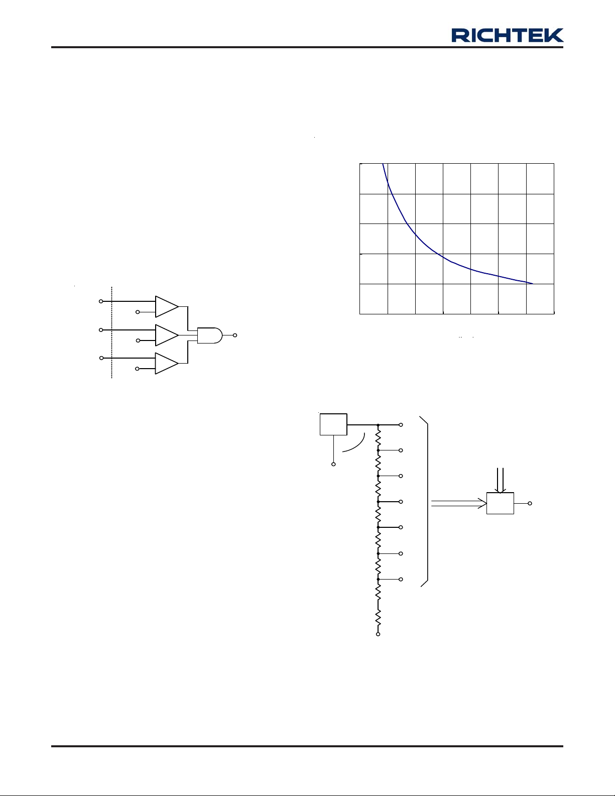
The phase switching frequency of the RT8841 is set by
an external resistor connected from the RT pin to GND.
The frequency follows the gra ph in Figure 2.
Power Ready Detection
During start-up, RT8841 will detect VCC12, VCC5 and VTT.
When VCC12 > 9.6V, VCC5 > 4.6V and VTT > 0.85V POR
will go high. POR (Power On Reset) is the internal signal
to indicate all voltage powers are ready to let RT8841 a nd
the companioned MOSFET drivers to work properly . When
POR = L, RT8841 will try to turn off both high side a nd low
side MOSFETs.
VCC12
VCC5
V
9.6V
4.6V
TT
0.85V
CMP
+
-
CMP
+
-
POR : Power On Reset
CMP
+
-
POR
Figure 1. Circuit for Power Ready Detection
Phase Detection
The number of operational phas e s is determined by the
internal circuitry that monitors the ISNx voltages during
start up. Normally, the RT8841 operates as a 4-phase
PWM controller. Pull ISN4 and ISP4 to VCC5 programs
3-phase operation, pull ISN3 a nd ISP3 to VCC5 programs
2-phase operation, and pull ISN2 and ISP2 to VCC5
programs 1-pha se operation. RT8841 detects the voltage
of ISN4, ISN3 and ISN2 at POR rising edge. At the rising
edge, RT8841 detects whether the voltage of ISN4, ISN3
and ISN2 are higher than “VCC5 − 1V” respectively to
decide how many phases should be active. Phase
detection is only active during start up. When POR = H,
the number of operational phases is determined and
latched.
Frequency vs. R
1000
800
600
400
Frequency ( kHz)
200
0
0 10203040506070
R
(k)
(kΩ)
RT
Figure 2. RRT vs Phase Switching Frequency
V
Gnerator
DAC
VGB
FBRTN
+
16V
-
FBRTN
Figure 3. V
R1
R2
R3
R4
R5
R6
R7
R8
1.6V
1.4V
1.2V
0.5V to 1.6V
Step = 6.25mV
1.0V
0.8V
0.6V
0.4V
Generator Circuit
DAC
RT
VID[7:0]
MUX
V
DAC
22
DS8841-02C September 2007www.richtek.com
Page 23
Conceptual
RT8841
RT8841 builds a precise bandga p reference circuit inside.
The output voltage of bandga p reference is 1.6V referred
to FBRTN. In Figure 3, RT8841 uses plural resistors to
generate precise reference voltages ranging from 0.5V to
1.6V. All the voltages connect to a multiplexer (MUX).
According to the VID inputs, multiplexer outputs the
selected voltage, V
. Please be careful that all the
DAC
voltage values in Figure 3 are referred to FBRT N.
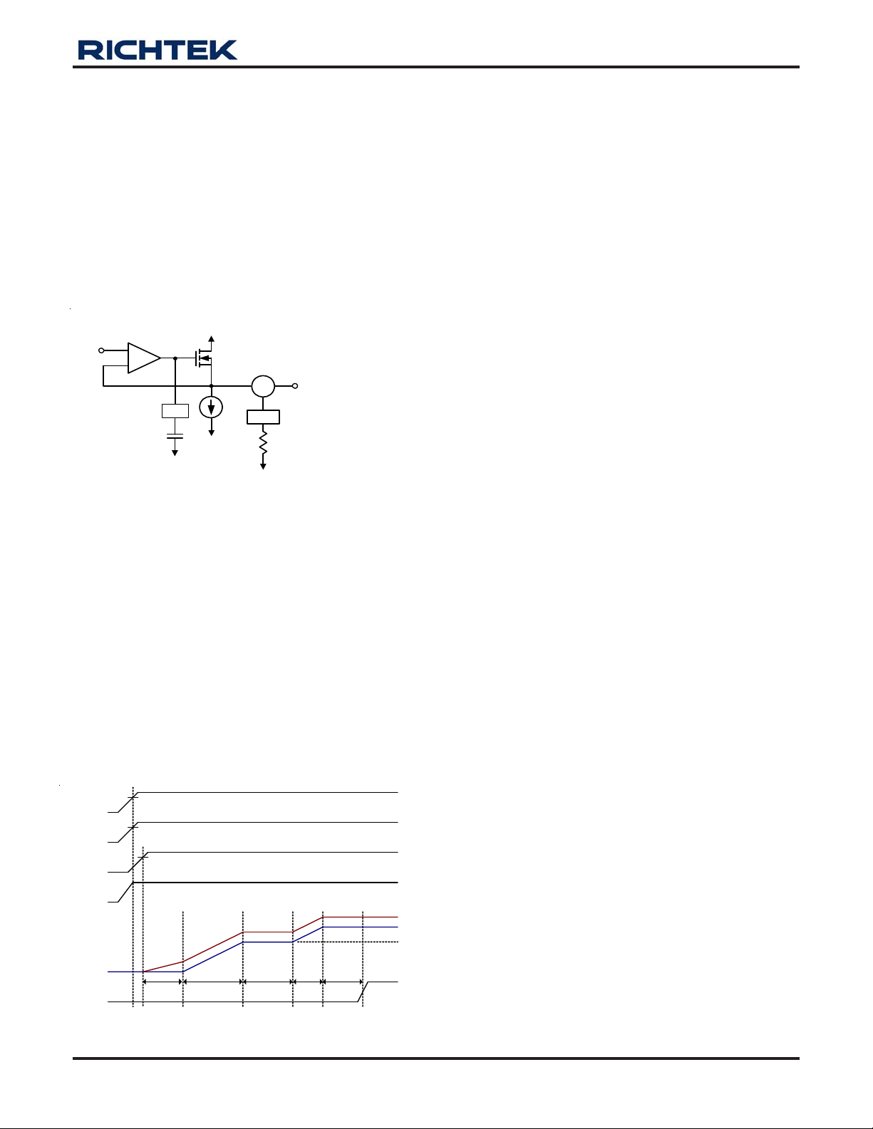
Soft Start
Output current of OPSS (I
V
DAC
OPSS
+
-
C
SS
SS
) is limited and variant
SS
SSQ
+
-
ADJ
R
ADJ
NTC
EAP
(ErrorAmp positive input)
Figure 4. Circuit for Soft Start and Dyn amic VID
The V
start-up time is set by a capacitor from the SS
OUT
pin to GND. In power_on_re set state (POR = L), the SS
pin is held at GND. After power_on_reset stae (POR = H)
and a n extra delay 1600μs, VSS and V
V
SSQ
= V
BOOT
. When V
SSQ
= V
BOOT
begin to rise till
SSQ
, RT8841 stays in this
state for 800μs waiting for valid VID code sent by CPU.
After receiving valid VID code, V
continues ramping up
OUT
or down to the voltage specified by VID code. Before
PWRGD = H, output current of OPSS (ISS) is limited to
8μA (ISS1). When PW RGD = H, ISS is limited to 80μA (ISS2).
The soft start waveform is shown in Figure 5.
V
TT
V
CC
VCC12
5
0.85V
4.6V
UVLO
THRESHOLD
will trace V
V
OUT
V
is a small voltage signal which is proportional to
ADJ
I
. This voltage is used to generate loadline a nd will be
OUT
which is equal to “V
EAP
SSQ
− V
ADJ
”.
described later. T1 is the delay time from power_on_reset
state to the beginning of V
OUT
rising.
T1 = 1600μs + 0.6V x CSS/ISS1 (1)
T2 is the soft start time from V
T2 = V
x CSS/ISS1 (2)
BOOT
T3 is the dwelling time for V
T4 is the soft start time from V
V
.
DAC
T4 ~= |V
DAC
− V
| x CSS/ISS1 (3)
BOOT
OUT
= 0 to V
OUT
= V
OUT
. T3 = 800μs.
BOOT
= V
BOOT
OUT
= V
to V
BOOT
OUT
=
T5 is the power good delay time, T5 ~= 1600μs.
Dynamic VID
The RT8841 can accept VID input changing while the
controller is running. This allows the output voltage (V
OUT
to change while the DC/DC converter is running and
supplying current to the load. This is commonly referred
to as VID on-the-fly (OTF). A VID OTF can occur under
either light or heavy load conditions. The CPU changes
the VID inputs in multiple steps from the start code to the
finish code. This change can be positive or negative.
Theoretically, V
should follow V
OUT
which is a staircase
DAC
waveform. In RT8841, a s mentioned in soft start session,
V
slew rate is limited by ISS2/CSS when PWR GD = H.
DAC
This slew rate limiter works as a low pass filter of V
and makes the bandwidth of V
smoothening V
staircase wavef orm, V
DAC
waveform finite. By
DAC
will no longer
OUT
DAC
overshoot or undershoot. On the other hand, CSS will
increase the settling ti me of V
during VID OTF . In most
OUT
cas es, 1nF to 30nF cera mic capa citor is suitable for CSS.
.
)
V
DAC
V
SS
SSQ
PWRGD
T1 T2 T3
T4 T5
BOOT
Figure 5. Soft Start Waveforms
DS8841-02C September 2007 www.richtek.com
23
Page 24
RT8841
Conceptual
Output Voltage Differential Sensing
C2
C
FB
R
V
CCP
(Positive remote
sense pin of CPU)
(Negative remote
sense pin of CPU)
V
CCN
FB
R
ADJ
Figure 6. Circuit for V
FB
I
OFSP
-
EA
+
+
V
DAC
-
FBRTN
ADJ
Differential Sensing and No
OUT
+
-
EAP
R1
I
OFSN
C1
COMP
Load Offset
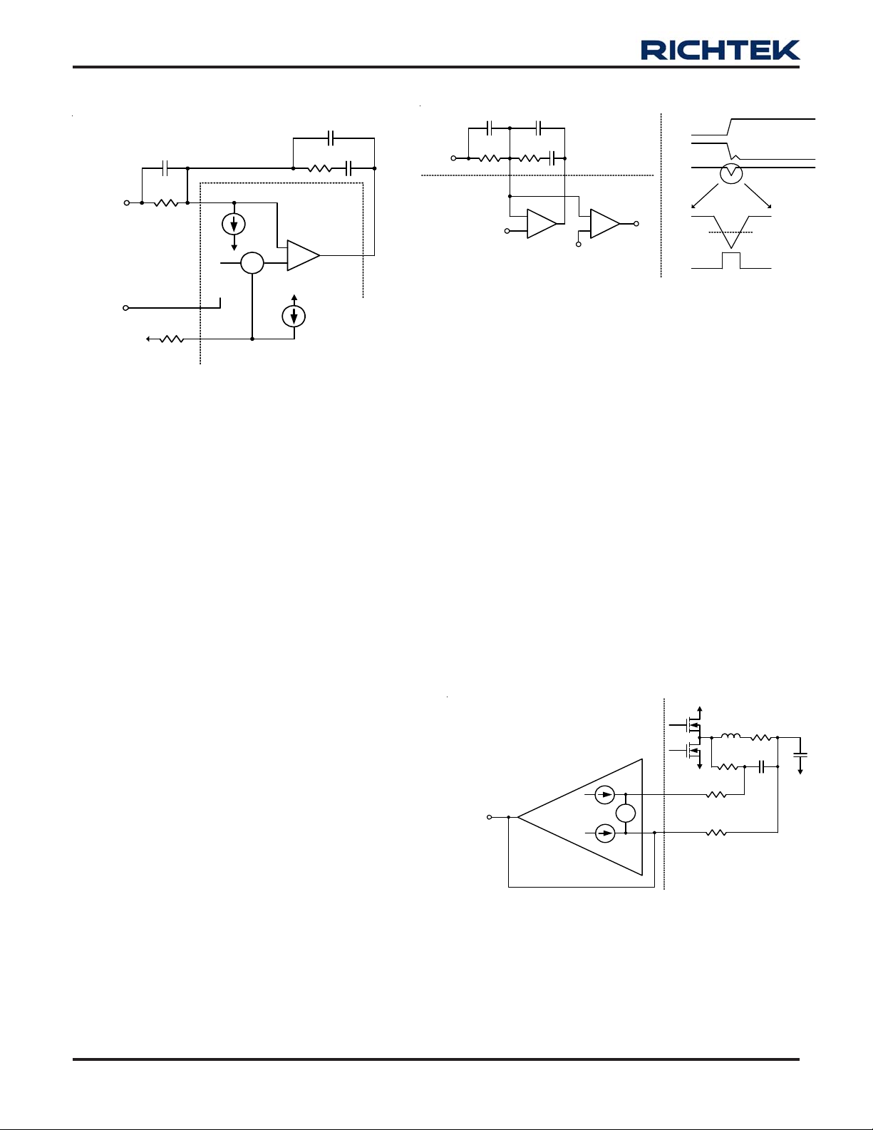
The RT8841 uses differential sensing by a high gain low
offset ErrorAmp. The CPU voltage is sensed between the
FB and FBRT N pins. A resistor (RFB) connects FB pin and
the positive remote sense pin of the CPU (V
). FBRT N
CCP
pin connects to the negative remote sense pin of CPU
(V
) directly. The ErrorAmp compares EAP (= V
CCN
V
) with the VFB to regulate the output voltage.
ADJ
DAC
−
No-Load Offset
In Figure 6, I
offset. Either I
Connect a resistor from OFS pin to G ND to a ctivate I
I
flows through R
OFSN
case, negative no-loa d offset voltage (V
V
= I
OFSN
OFSN
Connect a resistor from OFS pin to VCC5 to activate I
I
flows through RFB from the V
OFSP
case, positive no-loa d offset voltage (V
V
= I
OFSP
OFSP
OFSN
OFSN
x R
and I
or I
ADJ
are used to generate no-load
OFSP
is active during normal operation.
OFSP
from ADJ pin to GND. In this
ADJ
= 0.8 x R
x RFB = 6.4 x RFB/R
) is generated.
OFSN
ADJ/ROFS
(4)
to FB pin. In this
CCP
) is generated.
OFSP
(5)
OFS
OFSN
OFSP
Load Transient Quick Response
C
V
OUT
EAP = VQR- V
FB
R
FB
ADJ
C2
C1
R1
FB COMP
+
EAP - V
QR
I
OUT
V
OUT
FB
+
QR
FB
QR
Figure 7. Load Tr ansient Quick Respon se
In steady state, the voltage of VFB is controlled to be very
close to V
to heavy load could cause VFB lower than V
. While a load step tra n sient from light loa d
EAP
EAP
tens of mV. In prior design, owing to limited control
bandwidth, controller is hard to prevent V
OUT
during quick load tran sient from light load to heavy loa d.
RT8841 detects load tran sient by comparing VFB and V
If VFB suddenly drops below “V
− VQR”, VQR is a
EAP
predetermined voltage. The quick response indicator QR
rises up. When QR = H, RT8841 turns on all high side
MOSFETs and turn off all low side MOSFETs. The
sensitivity of quick response can be a djusted by the values
of CFB and RFB. Smaller RFB and/or larger CFB will make
QR ea sier to be triggered. Figure 7 is the circuit and typical
waveforms.
Output Current Sensing
.
.
CSA: Current Sense Amplifier
I
X
235nA
V
OFS_CSA
235nA
+
+
-
-
ISP
ISN
R
CSP
R
CSN
= V
= V
EAP
by several
undershoot
EAP
L
DCR
C
R
S
S
EAP
- V
QR
.
24
Figure 8. Circuit for Channel Current Sensing
DS8841-02C September 2007www.richtek.com
Page 25
Conceptual
RT8841
The RT8841 provides low input offset current-sense
amplifier (CSA) to monitor the output current of every
channel. Output current of CSA (I
[n]) is used for channel
X
current balance a nd active voltage position. In this inductor
current sensing topology , RS and CS must be set according
to the equation below :
L/DCR = RS x CS (6)
Then the output current of CSA will follow the equation
below :
IX = [IL x DCR − V
OFS-CSA
+ 235n x (R
CSP
− R
CSN
)]/R
CSN
(7)
235nA is typical value of CSA input offset current.
V
OFS-CSA
RT8841 is smaller than +/- 1mV. Usually, “V
235n x (R
is the input offset voltage of CSA. V
CSP
− R
)” is negligible except at very light
CSN
OFS-CSA
OFS-CSA
of
+
load and the equation can be simplified as the equation
below :
IX = IL x DCR/R
(8)
CSN
Loadline
Output current of CSA is summed and averaged in
RT8841. Then 0.5Σ(IX[n]) is sent to ADJ pin. Because
ΣIX[n] is a PTC (Positive T emperature Coef ficient) current,
an NTC (Negative Temperature Coefficient) resistor is
needed to connect ADJ pin to GND. If the NTC resistor is
properly selected to compensate the temperature
coefficient of IX[n], the voltage on ADJ pin will be
proportional to I
the positive input of ErrorAmp is “V
follow “V
DAC
decreasing linearly with I
without temperature effect. In RT8841,
OUT
− V
− V
DAC
”, too. Thus, the output voltage
ADJ
is obtained. The loadline is
OUT
ADJ
”. V
OUT
will
defined as
LL(loadline) = ΔV
= 0.5 x DCR x R
OUT
/ΔI
OUT
= ΔV
ADJ/RCSN
ADJ
/ΔI
OUT
(9)
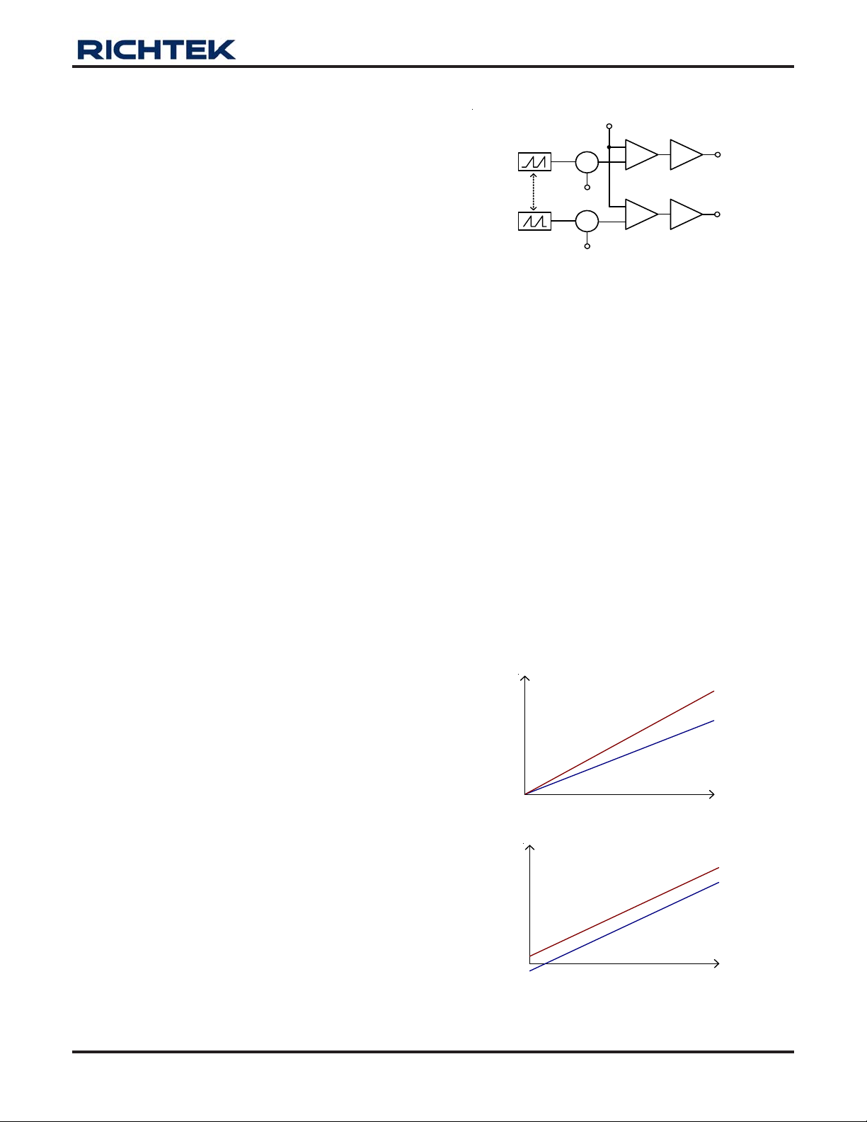
Current Balance
COMP
RAMP[1]
Interleaved
RAMP[n]
I
ERR
I
ERR
+
-
[1] x R
+
-
[n] x R
CB
CB
+
CMP
-
+
CMP
-
BUF
BUF
PWM[1]
PWM[n]
Figure 9. Circuit for Channel Current Bala nce
In Figure 8, IX[n] is the current signal which is proportional
to current flowing through channel n. In Figure 9, the
current error signals I
[n] (= IX[n] − AV G(IX[n])) are used
ERR
to raise or lower the internal sawtooth waveforms
(RAMP[1] to RAMP[n]) which are compared with ErrorAmp
output (COMP) to generate PWM signal. The raised
sawtooth waveform will decrease the PWM duty of the
corresponding channel while the lowered will increase.
Eventually , current flowing through each channel will be
balanced.
Channel Current Adjust
If channel current is not bala nced due to asymmetric PCB
layout of power stage, external resistors can be adjusted
to correct current imbalance. Figure 10 shows two types
of current imbalance, constant ratio type and constant
difference type.
I1
I2
I
, total
OUT
Constant ra tio
Briefly, the resistance of R
loadline. The temperature coefficient of R
sets the resistance of
ADJ
compensates
ADJ
I1
the temperature effect of loadline.
I2
I
, total
OUT
Constant difference
Figure 10. Channel Current vs. Total Current
DS8841-02C September 2007 www.richtek.com
25
Page 26
RT8841
Conceptual
If the initial current distribution is constant ratio type,
according to Equation(8), reduce R
[1] can reduce IL[1]
CSN
and improve current bala nce. If the initial current distribution
is constant difference type, according to Equation(7),
increase R
[1] can reduce IL[1] and improve current
CSP
balance.
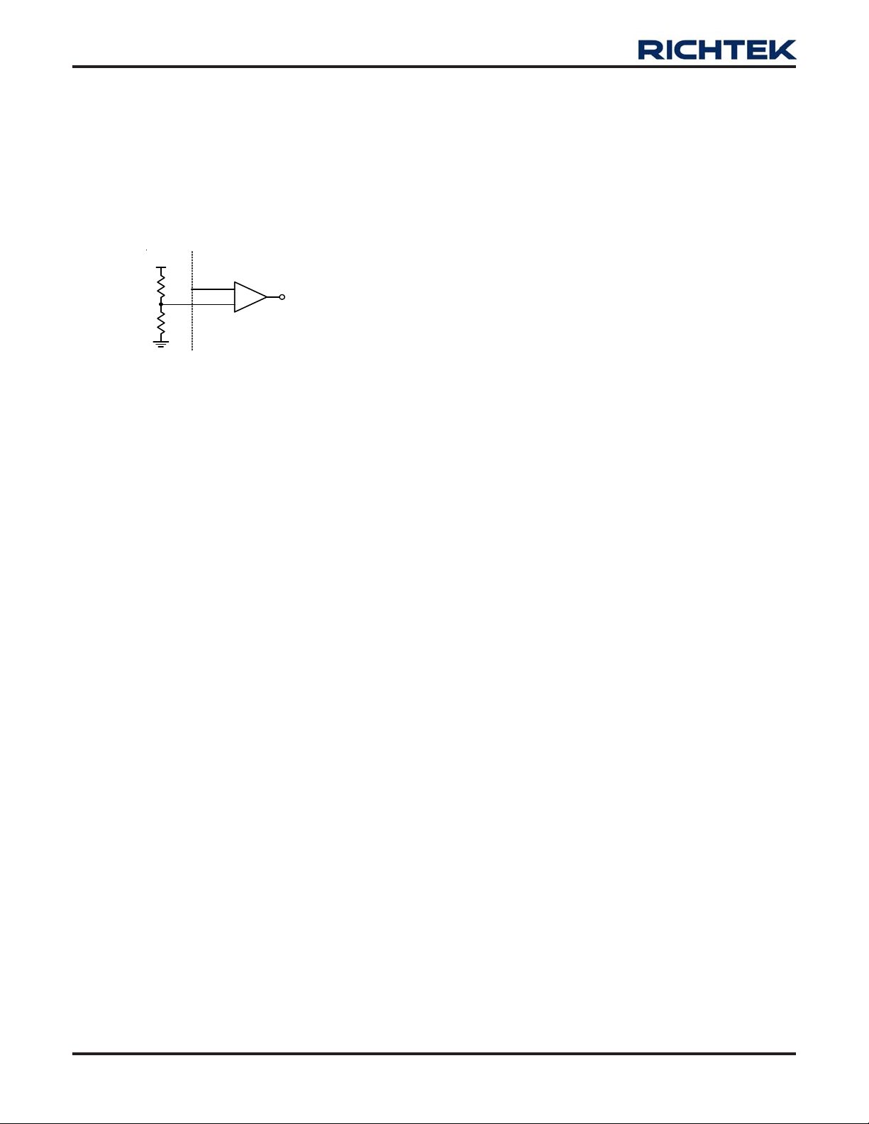
Over Current Protection (OCP)
VCC5
ADJ
R1
R2
IMAX
+
CMP
-
OCP
Figure 1 1. Over Current Protection
In Figure 11, V
RT8841, V
ADJ
compensated. Once V
is equal to 5V x R2/(R1 + R2). In
IMAX
is proportional to I
is larger than V
ADJ
and is thermally
OUT
IMAX
, OCP is
triggered and latched. RT8841 will turn off both high side
MOSFET and low side MOSFET of all cha nnels. A 20uS
delay is used in OCP detection circuit to prevent false
trigger.
Over Voltage Protectiom (OVP)
The over voltage protection monitors the output voltage
via the FB pin. Once VFB exceeds “V
+ 150mV”, OVP
EAP
is triggered and latched. RT8841 will try to turn on low
side MOSFET and turn of f high side MOSFET to protect
CPU. A 20μs delay is used in OVP detection circuit to
prevent false trigger.
26
DS8841-02C September 2007www.richtek.com
Page 27

Conceptual
RT8841
Datasheet Revision History
Version Data Page No. Item Description
00C 2007/5/25 First Edition
01C 2007/7/30
02C 2007/9/14
Pin Configurations
Typical Operati ng Characteristics
Application Information
Pin Configurations
Fu nct ion Block
Modify
Add Curve
Modify pin10.
DS8841-02C September 2007 www.richtek.com
27
Page 28
RT8841
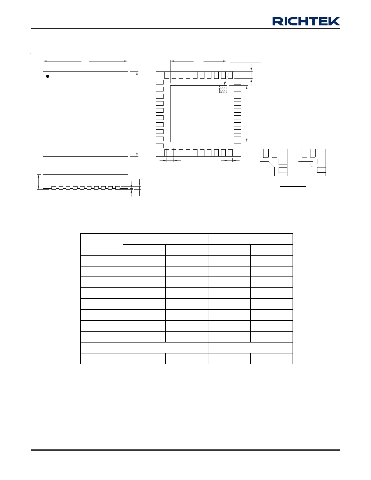
Outline Dimension
Conceptual
D
E
e
A
A3
A1
D2
SEE DETAIL A
L
1
E2
1
b
2
DETAIL A
Pin #1 ID a nd T ie Bar Mark Option s
1
2
Note : The configuration of the Pin #1 identifier is optional,
but must be located within the zone indicated.
Symbol
Dimensions In Millimeters Dimensions In Inches
A 0.700 0.800 0.028 0.031
A1 0.000 0.050 0.000 0.002
A3 0.175 0.250 0.007 0.010
b 0.180 0.300 0.007 0.012
D 5.950 6.050 0.234 0.238
D2 4.000 4.750 0.157 0.187
E 5.950 6.050 0.234 0.238
E2 4.000 4.750 0.157 0.187
e 0.500 0.020
L 0.350 0.450
Richtek Technology Corporation
Headquarter
5F, No. 20, Taiyuen Street, Chupei City
Hsinchu, Taiwan, R.O.C.
Tel: (8863)5526789 Fax: (8863)5526611
Min Max Min Max
0.014 0.018
W-Type 40L QFN 6x6 Package
Richtek Technology Corporation
Taipei Office (Marketing)
8F, No. 137, Lane 235, Paochiao Road, Hsintien City
Taipei County, Taiwan, R.O.C.
Tel: (8862)89191466 Fax: (8862)89191465
Email: [email protected]
28
DS8841-02C September 2007www.richtek.com
 Loading...