

Page 1

Two Phases Synchronous Buck PWM Controller
RT8807/A
General Description
The RT8807/A is a two phases synchronous Buck PWM
controller with integrated drivers which is optimized for
high-performance graphic microprocessor and computer
applications. The IC integrates a voltage mode PWM
controller, two 5V MOSFET drivers with internal bootstrap
diodes, as well as output current monitoring and protection
functions into the V/WQFN-24L 4x4 package.
The inductor currents are sensed by lossless DCR current
sensing technique for current balance and over current
protection. The RT8807/A also features a reference tracking
mode operation in which the feedback voltage is regulated
and tracks external input reference voltage. Other features
include output current indication, adjustable operating
frequency, adjustable soft-start, power good, external
compensation, and enable/shutdown functions.
Ordering Information
RT8807
Package Type
QV : VQFN-24L 4x4 (V-Type)
Operating Temperature Range
P : Pb Free with Commercial Standard
G : Green (Halogen Free with Commer cial Standard)
RT8807A
Package Type
QW : WQFN-24L 4x4 (W-Type)
Features
zz
z Two-Phase Power Conversion with Single 12V
zz
Power Supply
zz
z Embedded 5V Upper Gate Driver and 12V Lower
zz
Gate Driver
zz
z Internal Regulated 5V Output
zz
zz
z Precise Core Voltage Regulation
zz
zz
z Selectable Internal / External Reference
zz
zz
z Differential Inductor DCR Current Sense
zz
zz
z External Programmable Voltage Droop Control
zz
zz
z Enable Control for External Shutdown
zz
zz
z Adjustable Operating Frequency
zz
zz
z Adjustable Soft Start
zz
zz
z Power Good and Output Current Indication
zz
zz
z Adjustable Over Current Protection
zz
zz
z Over Voltage Protection
zz
zz
z Under Voltage Protection
zz
zz
z Over Temperature Protection
zz
zz
z Proprietary BTR (Boost Transient Response)
zz
Feature Reducing Output V oltage Drop During Load
Tra nsition (For RT8807 Only)
zz
z RoHS Compliant and 100% Lead(Pb)-Free
zz
Applications
z Middle to High End GPU Core Power
z High End Desktop PC Memory Core Power
z Low Voltage, High Current DC / DC Converter
z Voltage Regulator Modules
Operating Temperature Range
G : Green (Halogen Free with Commer cial Standard)
Note :
Richtek Pb-free and Green products are :
Marking Information
For marking information, contact our sales representative
directly or through a Richtek distributor located in your
area, otherwise visit our website for detail.
`RoHS compliant and compatible with the current require-
ments of IPC/JEDEC J-STD-020.
`Suitable for use in SnPb or Pb-free soldering processes.
`100% matte tin (Sn) plating.
DS8807/A-00 April 2008 www.richtek.com
1
Page 2
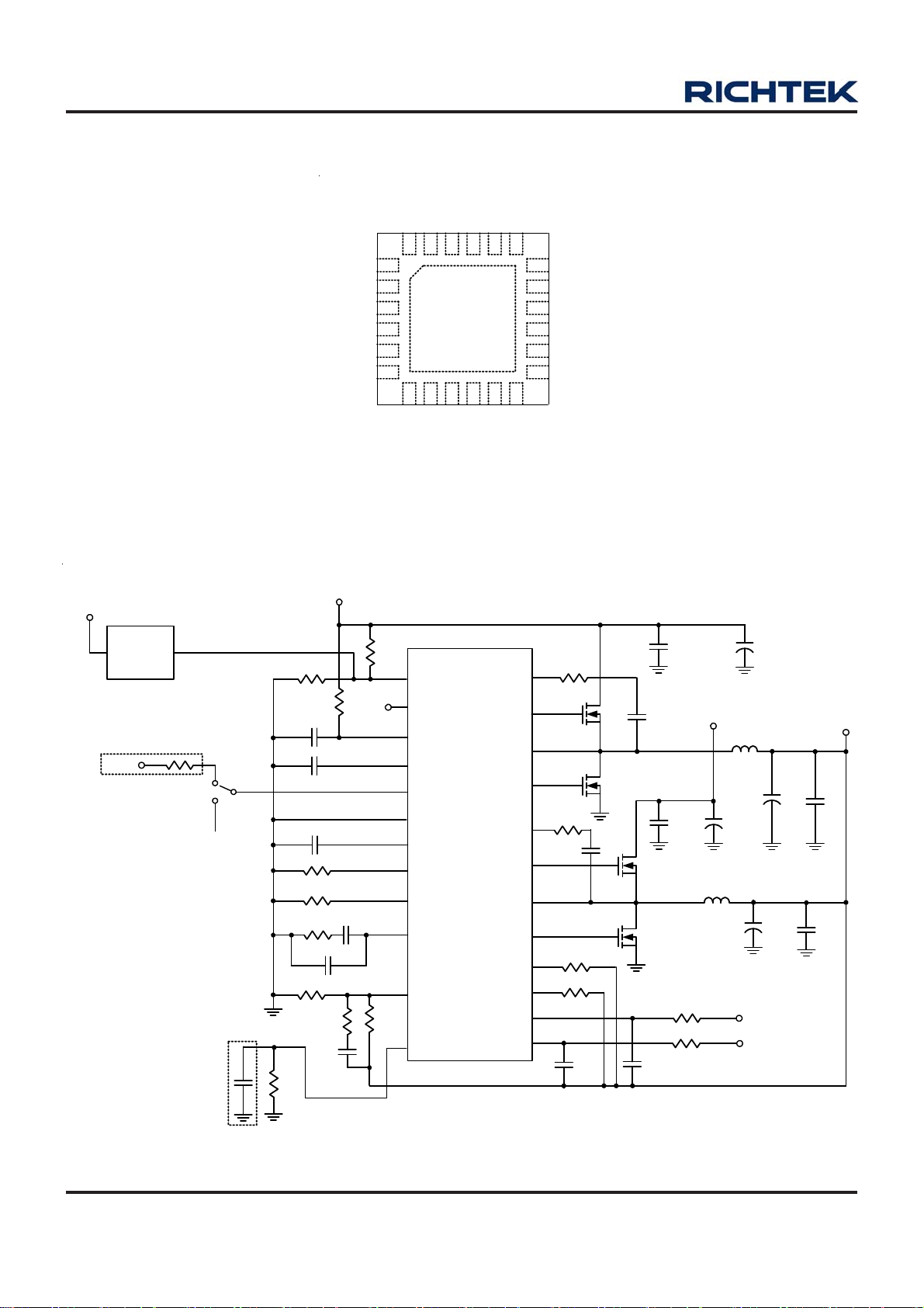
RT8807/A
Pin Configurations
UGATE1
BOOT1
Typical Application Circuit
5VCC
AGND
EN2B
CSP1
(TOP VIEW)
PHASE1
LGATE1
VCC
24 2223
1
2
3
4
5
6
PGND
7
8910 12
CSP2
CSN1
CSN2
V/WQFN-24L 4x4
DROOP
LGATE2
21 20 19
25
11
RT
IOUT/IMAX
PHASE2
18
UGATE2
17
BOOT2
16
REFOUT/PGOOD
15
REFIN/EN
14
SS
13
FB
COMP
EXT_12V
EXT_12V
DET
Circuits
Internal Reference mode
5V
CC
External Reference
Voltage (0.45 to 2.5V)
EXT_12V_DETB
Optional
Optional
R9
R2
R7
C1
R6
C18
V
12V
C2
C3
R16
R4
R5
CC
C5
R3
C4
R1
R8
5
16
22
3
15
4
14
11
10
12
13
21
RT8807/A
EN2B
REFOUT/
PGOOD
VCC
5VCC
REFIN/
EN
AGND
SS
RT
IOUT/
IMAX
COMP
FB
DROOP
BOOT1
UGATE1
PHASE1
LGATE1
BOOT2
UGATE2
PHASE2
LGATE2
CSN2
CSN1
CSP2
CSP1
2
1
24
23
17
18
19
20
8
7
9
6
R14
R15
R10
R11
C16
C9
Q1
Q2
Q3
Q4
C17
C8
C6
EXT_12V
/V
C10
R12
R13
CC
L2
12V
+
C11
+
C7
L1
+
C14
PHASE2
PHASE1
+
C12
C13
C15
V
OUT
Figure 1. Typical Application Circuit with 12V Input
DS8807/A-00 April 2008www.richtek.com
2
Page 3
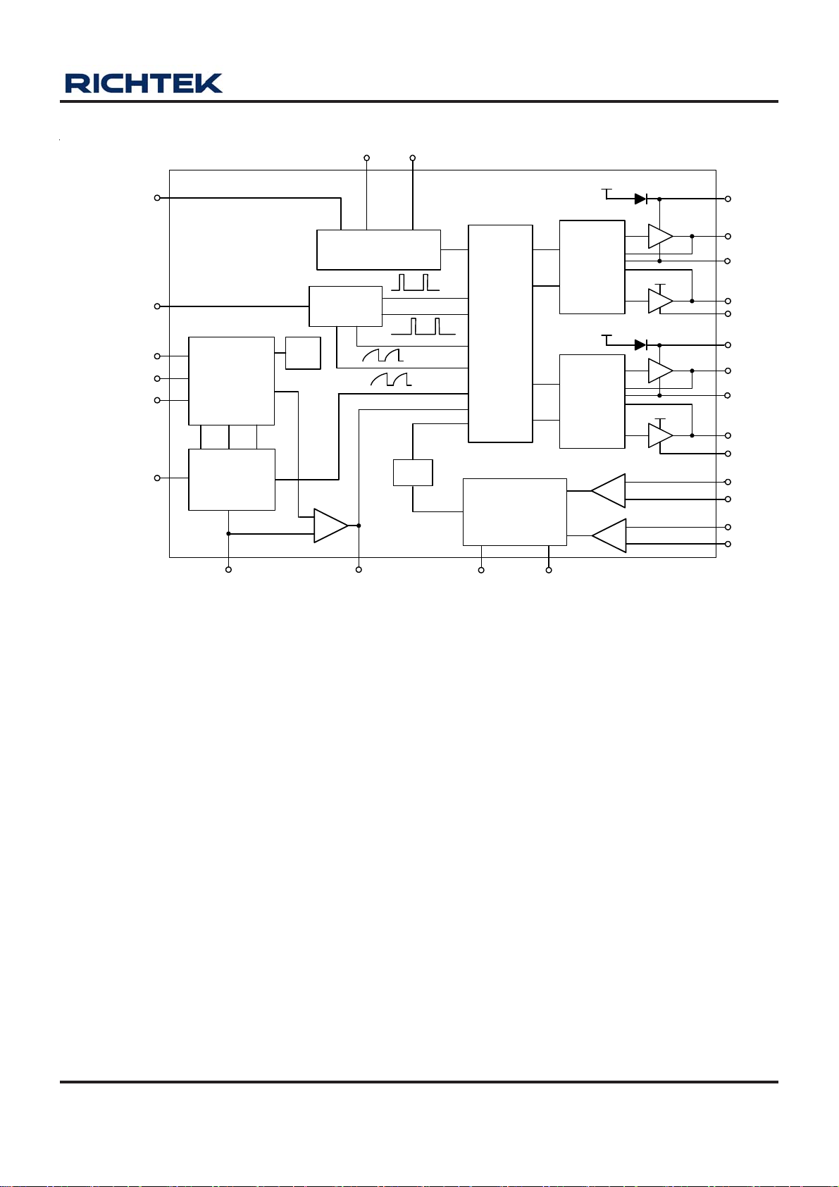
Function Block Diagram
VCC
5VCC
RT8807/A
EN2B
5VCC
BOOT1
Gate
Control
Logic &
Shoot
Through
Prevention
5VCC
Gate
Control
Logic &
Shoot
Through
Prevention
GM1
GM2
RT
REFIN/EN
SS
AGND
REFOUT/PGOOD
REF Select
Soft Start
REF Buffer
50% 75% 115%
UV/OV
Protection &
PGOOD
FB COMP
0.6V
REF
5VCC Regulator &
Power On Reset
Oscillator &
Ramp
Generator
Error
Amplifier
+
-
Pulse
Width
Modulator
& Central
Control
Logic
OCP
Current SENSE
IOUT/IMAX DROOP
Power up scheme to support dual power rails application
UGATE1
PHASE1
VCC
LGATE1
PGND
BOOT2
UGATE2
PHASE2
VCC
LGATE2
PGND
+
-
+
-
CSP1
CSN1
CSP2
CSN2
This feature is to support the following case in the application where one phase is powered by PCIEBUS_12V and the
other phase is powered by EXT_12V.
`When the system is powered without EXT_12V Cable, RT8807/A will work with one phase and be able to boot system
into Dos Warning screen.
`The Warning message tells user to power off the system first, plug in the EXT_12V Cable, and then reboot the system
again.
`After system re-boot, RT8807/A could work with two phases.
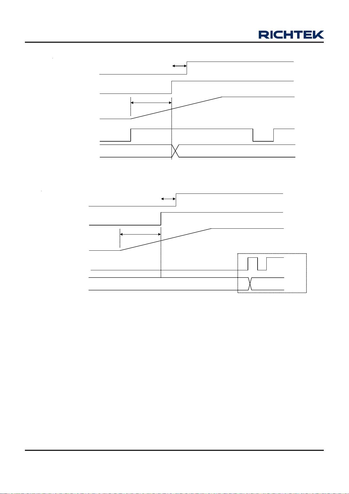
Below is the power up sequence for dual VIN (PCIEBUS_12V & EXT_12V) application. This a pplication is cla ssified
into two case s :
<1> The external connector is not plugged while power on
The EXT_12V_DETB is pulled up to High. Soft-start will be released to ramp up after POR. After T1, RT8807/A latches
EN2B signal and determines to operate in single phase. The time interval T1 is used to wait EN2B ready. Once single
phase is confirmed, the external 12V power connector plugged or not will not affect the status.
<2> The external connector is plugged while power on
The EXT_12V_DETB is grounded by external cable detection circuits. RT8807/A latches EN2B at T1 and determines to
operate in two phases. If the connector is removed later, RT8807/A will turn off phase 2 and enter single phase operation
mode. Further plugged in/out will not affect the status anymore.
DS8807/A-00 April 2008 www.richtek.com
3
Page 4
RT8807/A
First PWM Pulse
Detection Latch Signal
V
IN
EN2B/EXT_12V_DETb
~us
T1
Soft-Start
One/Two Phase Operation
First PWM Pulse
Detection Latch Signal
V
IN
Soft-Start
EN2B/EXT_12V_DETb
One/Two Phase Operation
Figure 2. External Connector is not Plugged
~us
T1
Two Phase
Figure 3. External Connector is Plugged
One PhaseTwo Phase
One Phase
DS8807/A-00 April 2008www.richtek.com
4
Page 5

Functional Pin Description
RT8807/A
UGA TE1 (Pin 1), UGA TE2 (Pin 18)
Upper Gate Drivers. Theses pins provide the gate drive for
the converter's high-side MOSFET. Connect these pins
to the high-side MOSFET gate.
BOOT1 (Pin 2), BOOT2 (Pin 17)
Bootstrap Power Pins. Theses pins power the high-side
MOSFET drivers.
5VCC (Pin 3)
Internal Regulator Power Pin. The regulated voltage
provides power supply for all low-voltage circuits. Bypass
at least 1uF ceramic capacitor to sustain high PSRR.
AGND (Pin 4)
Signal ground for the IC. All voltage levels are measured
with respect to this pin.
EN2B (Pin 5)
EXT_12V Detection Pin. RT8807/A latches high/low status
of this pin in soft start period. If the result is low, RT8807/
A will enter two phase operation. If it's high, RT8807/A
turns off phase2 and operate in single phase only.
FB (Pin 13)
Feedback Pin. This pin is connected to the PWM converter
output's voltage or a resistor divider. This pin also connects
to the inverting input of error amplifier and the PGOOD/
UV/OV detection circuits.
SS (Pin 14)
Soft-Start Pin. Connect a capacitor from this pin to ground
to set the soft-start interval.
REFIN/EN (Pin 15)
External Reference Input.
`If pulled up to 5VCC, internal reference is used (0.6V)
`If driven by external voltage ranged from 0.45V to 2.5V,
external reference is used
`If pulled below 0.4V, device is disabled.
REFOUT/PGOOD (Pin 16)
Reference Out and Power GOOD. This pin drives 1.15V
out once FB exceeds ~72.5% of the reference voltage
after soft- start ends. This pin keeps at this voltage
regardless of internal or external reference is used.
CSP1 (Pin 6), CSP2 (Pin 9)
These pins are positive input of current sensing
transconductance amplifiers 1 and 2.
CSN1 (Pin 7), CSN2 (Pin 8)
These pins are negative input of current sensing
transconductance amplifiers 1 and 2.
IOUT/IMAX (Pin10)
Output Current Indication. This pin sends a current out
(IX) referred to the sum of two sensed inductor currents
sense value. Connect this pin through a resistor to ground.
(I
= 4 x IX). This pin also sets maximum current limit
OUT
threshold.
RT (Pin11)
Frequency Timing Resistor. Connect a resistor from RT
to AGND to set the clock frequency.
COMP (Pin 12)
Compensation Pin. This pin is the output of the error amplifier.
DS8807/A-00 April 2008 www.richtek.com
PHASE1 (Pin 24) PHASE2 (Pin 19)
These pins are return nodes of the high-side driver.
Connect these pins to high-side MOSFET sources
together with the low-side MOSFET drain and the
inductors.
LGA TE1 (Pin 23), LGA TE2 (Pin 20)
Lower Gate Drivers. Theses pins provide the gate drive for
the converter's low-side MOSFET. Connect these pins to
the low-side MOSFET gate.
DROOP (Pin 21)
Set the load line for droop control. Connect this pin with a
resistor to ground.
VCC (Pin 22)
Provide a 12V supply voltage for the IC. Connect a
10Ω/1uF low pass filter to sustain high PSRR.
PGND [Exposed Pad (25)]
Power ground pin. Tie the synchronous PWM converter's
low-side MOSFET source to this pin.
5
Page 6

RT8807/A
C
C
Absolute Maximum Ratings (Note 1)
z Supply Voltage, V
z PHASE to GND
------------------------------------------------------------------------------------- −0.3V to 15V
CC
DC------------------------------------------------------------------------------------------------------------ −2V to 15V
< 200ns ----------------------------------------------------------------------------------------------------- −5V to 22V
z BOOT to PHASE ----------------------------------------------------------------------------------------- −0.3V to 7V
z BOOT to GND
DC------------------------------------------------------------------------------------------------------------ −0.3V to V
CC
< 200ns ----------------------------------------------------------------------------------------------------- −0.3V to 30V
z UGATE
DC------------------------------------------------------------------------------------------------------------ V
< 200ns ----------------------------------------------------------------------------------------------------- V
z LGATE
DC------------------------------------------------------------------------------------------------------------ −0.3V to V
< 200ns ----------------------------------------------------------------------------------------------------- −2V to V
z Other Input, Output or I/O Voltage -------------------------------------------------------------------- −0.3V to 7V
z Power Dissipation, P
D
@ T
= 25°C
A
PHASE
PHASE
−0.3V to V
−2V to V
CC
+ 0.3V
CC
V/WQFN−24L 4x4 ---------------------------------------------------------------------------------------- 1.923W
z Package Thermal Resistance (Note 4)
V/WQFN−24L 4x4, θJA---------------------------------------------------------------------------------- 52°C/W
z Lead Temperature (Soldering, 10 sec.) -------------------------------------------------------------- 260°C
z Junction Temperature ------------------------------------------------------------------------------------ 150°C
z Storage Temperature Range --------------------------------------------------------------------------- −40°C to 150°C
z ESD Susceptibility (Note 2)
HBM (Human Body Mode) ----------------------------------------------------------------------------- 2kV
MM (Machine Mode) ------------------------------------------------------------------------------------- 200V
+ 7V
BOOT
BOOT
+ 0.3V
+ 0.3V
+ 0.3V
Recommended Operating Conditions (Note 3)
z Supply Voltage -------------------------------------------------------------------------------------------- +12V ±10%
z Junction Temperature Range --------------------------------------------------------------------------- −40°C to 125°C
z Ambient Temperature Range --------------------------------------------------------------------------- −40°C to 85°C
Electrical Characteristics
(V
= 12V, PGND = 0V, TA = 25°C, unless otherwise specified)
IN
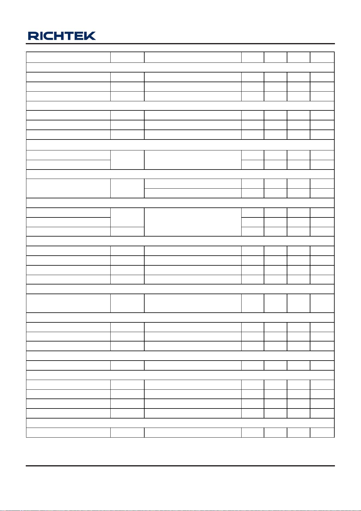
Parameter Symbol Test Conditions Min Typ Max Units
VCC Supply Input
VCC Supply Voltage
VCC Supply Current
5 VCC Su pply Out put
5VCC Supply Voltage V
5VCC Output So urcing I
6
V
CC
I
CC
5VCC
5VC
10.8 12 13.2 V
REFIN/EN = 0V (static) -- 5 -- mA
VCC = 12V 4.8 5.15 5.5 V
V
= 12V 20 -- -- mA
C
To be continued
DS8807/A-00 April 2008www.richtek.com
Page 7
RT8807/A
T
Parameter Symbol Test Conditions Min Typ Max Units
Power-On Reset
VCC Rising Threshold V
VCC H ysteresis V
EN2B High Threshold V
REFIN/EN
Enable Rising Threshold V
Enable Hysteresis V
REFIN Tracking Ran ge 0.45 -- 2.5 V
Reference Voltage Accuracy (use Internal Reference)
VCC Rising 6.7 7.5 8.3 V
VCCTH
-- 0.45 -- V
VCCHY
EN2B Rising 1 1.15 1.3 V
EN2BTH
REFIN/E N Rising 0.35 0.4 0.45 V
ENTH
-- 5 0 - - m V
ENHYS
Reference Voltage
Accuracy −1.5 -- +1.5 %
V
REF
REFIN Pull-High to 5VCC
FB Cou pled to COMP
0.591 0.6 0.609 V
Reference Voltage Accuracy (use External Reference)
V
= 0.45V to 0.6 V −6 -- +6 mV
Accuracy
RE FIN
V
= 0.6V to 2.5V −1 -- +1 %
RE FIN
REFOUT / PGOOD
REFOUT/PGOOD Voltage
Accuracy −2 -- +2 %
REFOUT Output Sourcing I
V
REF OUT
REFOU
> 75% of Reference Voltage
V
FB
3 5 -- mA
1.127 1.15 1.173 V
Error Amplifier
DC Gain ADC No load -- 70 -- dB
Gain-Bandwidth GBW C
Slew Rate SR C
= 10pF -- 8 -- MHz
LOAD
= 10pF 5 -- -- V/us
LOAD
Transconductance GM -- 24 00 -- uA/ V
Current Sense Amplifier
Max Current I
GM(MAX)
CS P
Sink Current from CSN
100 -- -- uA
= 1V
V
Oscillator
Running Frequency f
OS C
R
= 20kΩ 450 500 550 kHz
RT
Max Duty Cycle D 70 75 8 0 %
Ramp Amplitude ΔV
-- 2.6 -- V
RAMP
Soft Start
Soft Start Current ISS 14 20 30 uA
Protection
Over Current Th reshold V
Over-Vo ltag e Threshold V
Under-Voltage Threshold V
Over Te mperature Threshold T
Sweep I
OCP
Sweep FB Vo ltage 115 12 5 1 35 %
OVP
Sweep FB Voltage 45 5 5 6 3 %
UVP
-- 160 -- °C
OTP
OUT/IMAX
Voltage 2.07 2.3 2.53 V
Power GOOD
Active Threshold VFB Rising 65 72.5 80 %
To be continued
DS8807/A-00 April 2008 www.richtek.com
7
Page 8

RT8807/A
Parameter Symbol Test Conditions Min Typ Max Units
Gate Driver
Upper Drive Source R
Upper Drive Sink R
Lower Drive Source I
Lower Drive Sink R
Note 1. Stresses listed as the above "Absolute Maximum Ratings" may cause permanent damage to the device. These are for
stress ratings. Functional operation of the device at these or any other conditions beyond those indicated in the
operational sections of the specifications is not implied. Exposure to absolute maximum rating conditions for extended
periods may remain possibility to affect device reliability.
Note 2. Devices are ESD sensitive. Handling precaution is recommended.
Note 3. The device is not guaranteed to function outside its operating conditions.
Note 4. θ
is measured in the natural convection at TA = 25°C on a low effective thermal conductivity test board of
JA
JEDEC 51-3 thermal measurement standard.
USOU RC E
USI NK
LSOURCE
LSINK
BOOT − PHASE = 5V
250mA Source Current
BOOT − PHAS E = 5V
250mA Sin k Current
= 12V
V
CC
V
V
250mA Sin k Current
LGAT E
= 12V
CC
= 6 V
-- 1.5 3 Ω
-- 1.5 4 Ω
1 -- -- A
-- 0.9 2 Ω
DS8807/A-00 April 2008www.richtek.com
8
Page 9
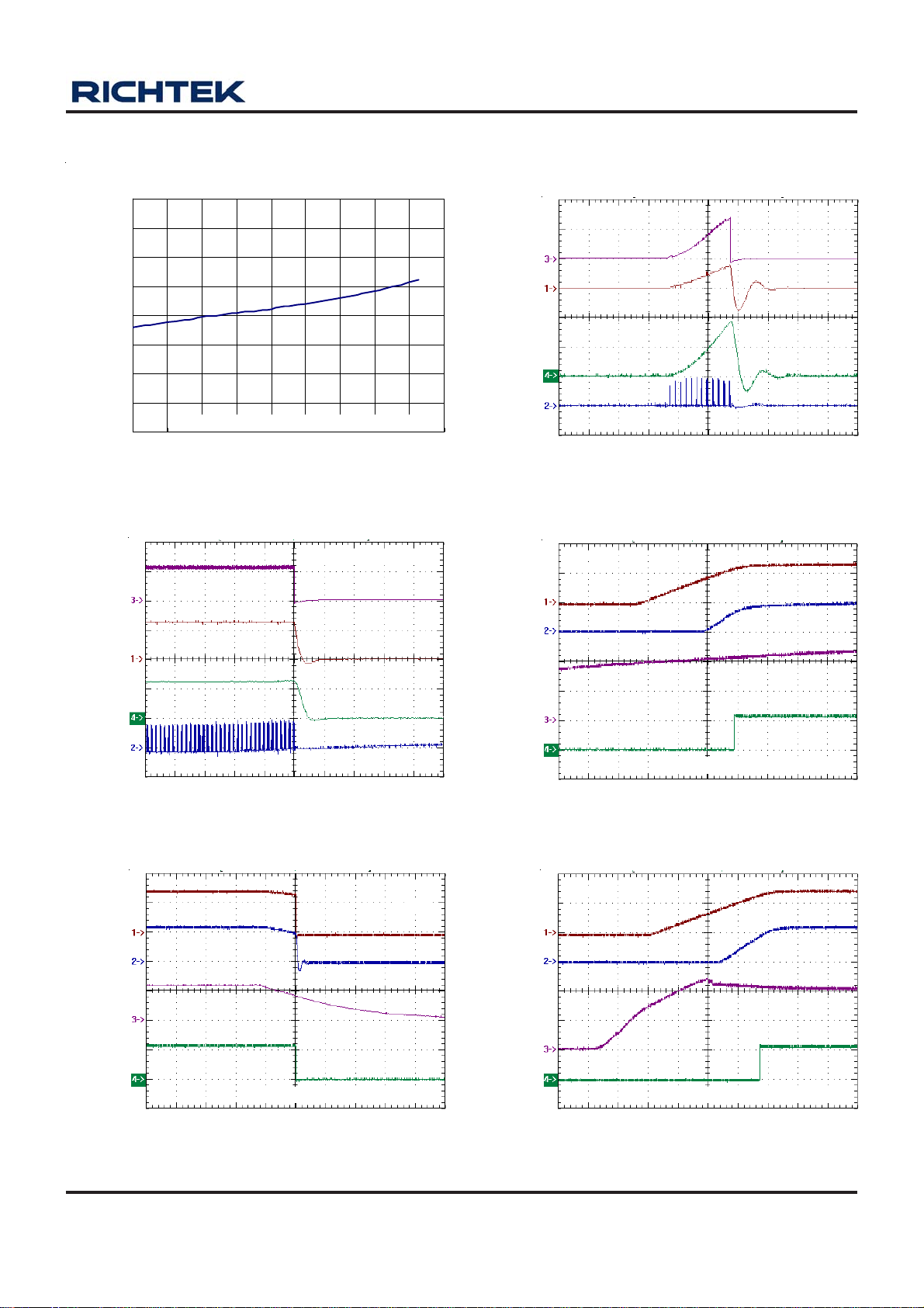
Typical Operating Characteristics
RT8807/A
430
420
410
400
390
380
370
Switching Frequency (kHz) 1
360
350
IOUT/IMAX
(2V/Div)
V
OUT
(1V/Div)
Switching Fre quency v s . Tem perature
V
= 12V, V
IN
-40 -20 0 20 40 60 80 100 120 140
= 1.2V, No Load, RRT = 26.1k
OUT
Temperature
(°C)
Over Current Protection
V
= 12V, V
IN
OUT
= 1.2V
IOUT/IMAX
(2V/Div)
V
OUT
(1V/Div)
I
LOAD
(50A/Div)
PHASE2
(10V/Div)
SS
(1V/Div)
V
OUT
(1V/Div)
Start Up in Short Circuit
V
= 12V
IN
Time (250us/Div)
Power On from REFIN
I
LOAD
(50A/Div)
PHASE2
(10V/Div)
SS
(1V/Div)
V
OUT
(1V/Div)
REFIN
(500mV/Div)
PGOOD
(1V/Div)
Time (250us/Div)
Power Off from REFIN
V
= 12V, V
IN
Time (1ms/Div)
OUT
= 1.2V, I
OUT
= 55A
REFIN
(200mV/Div)
PGOOD
(1V/Div)
SS
(1V/Div)
V
OUT
(1V/Div)
VCC
(5V/Div)
PGOOD
(1V/Div)
V
= 12V, V
IN
OUT
= 1.2V, I
Time (2ms/Div)
Power On from VCC
V
= 12V, V
IN
Time (2ms/Div)
OUT
= 1.2V, I
OUT
OUT
= 55A
= 55A
DS8807/A-00 April 2008 www.richtek.com
9
Page 10
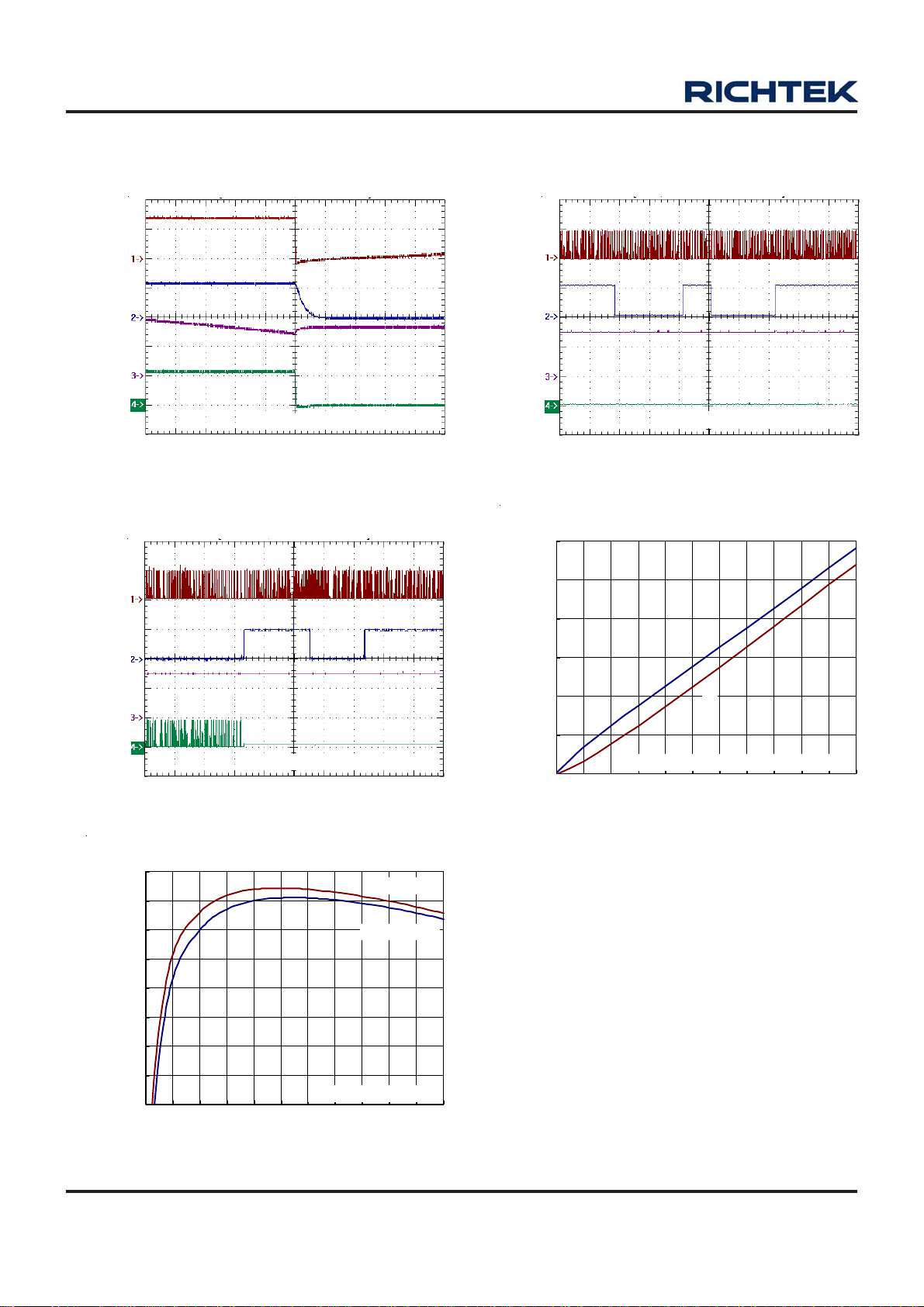
RT8807/A
SS
(1V/Div)
V
OUT
(1V/Div)
VCC
(5V/Div)
PGOOD
(1V/Div)
UGATE1
(20V/Div)
EN2B
(2V/Div)
Power Off from VCC
V
= 12V, V
IN
OUT
= 1.2V, I
OUT
Time (100us/Div)
Two-phase to Single-phase
= 55A
UGATE1
(20V/Div)
EN2B
(2V/Div)
V
OUT
(1V/Div)
UGATE2
(20V/Div)
Single-phase Operation
V
= 12V, V
IN
OUT
Time (50ms/Div)
Inductor Current vs. Output Current
30
25
20
I
L1
15
= 1.2V, No Load
V
OUT
(1V/Div)
UGATE2
(20V/Div)
Efficiency (%)
V
= 12V, V
IN
= 1.2V, No Load
OUT
Time (50ms/Div)
Efficiency vs. Output Current
90
85
80
75
70
65
60
55
V
50
0 5 10 15 20 25 30 35 40 45 50 55
Output Current (A)
= 12V, V
IN
FSW = 300kHz
FSW = 400kHz
OUT
= 1.2V
I
10
L2
Inductor Current (A)
5
V
= 12V, V
0
0 5 10 15 20 25 30 35 40 45 50 55
IN
= 1.2V, FSW = 400kHz
OUT
Output Current (A)
10
DS8807/A-00 April 2008www.richtek.com
Page 11

Application Information
The RT8807/A is a dual-phase voltage-mode synchronous
buck controller with embedded MOSFET drivers and
protection functions for low-voltage high-current
applications. The bootstrap diode is integrated into the IC
to reduce the external component count. In addition, the
number of operating phase (two-phase/single-phase) is
selectable to provide user with more flexibility in circuit
design. The inductor current is sensed by innovative DCR
current sensing technique for current balance and over
current protection.
Power On Reset
The RT8807/A initiates its soft start cycle only after the
IC power supply, VCC, and the internal regulated 5VCC
are ready. The internally regulated 5VCC is used for all of
the internal logic control circuit and the embedded high-
side MOSFET driver. The bootstrap diode for the high-
side MOSFET driver is integrated into the IC to reduce
the external component count. In addition, VCC is used
for the low-side MOSFET driver to reduce the R
the low-side MOSFET for enhanced efficiency
consideration.
The power on reset (POR) circuitry monitors the supply
voltage to ensure that the supply voltage is high enough
for controller's normal operation. Once VCC and 5VCC
exceed the POR rising threshold, the RT8807/A releases
the reset state, and works according to the settings.
Additionally, once any one of these two voltages is lower
than its POR falling threshold value, the chip turns off.
The hysteresis between the rising and falling thresholds
ensures that once the chip is enabled, it will not be
inadvertently turned off unless the bias voltage drops
substantially.
Soft Start and Power Good
Once the POR state is released, the soft start cycle
begins. A 20uA current source charges the capacitor, CSS,
which is connected between SS pin and GND to set the
soft start time. Figure 1 shows the power on sequence.
DS(ON)
of
RT8807/A
V
˜ 7.5V
VCCTH
V
CC
SS
V
OUT
PGOOD
Figure 1. Power on Sequence
During the soft start, the voltage on SS pin gradually
increases, and the output voltage of the error amplifier is
clamped to prevent the inrush current from the input
capacitors. Once the output voltage exceeds the power
good threshold level (72.5% of output voltage), REFOUT/
PGOOD pin will drive and maintain an reference voltage
1.15V unless VCC falls below POR threshold or Under
Voltage occurs.
Internal/External Reference
The RT8807/A supports the selectable internal/external
reference voltage to provide more flexibility in practical
applications. The selection of the internal/external
reference is described in detail as follows.
a. Using Internal Reference
The internal reference voltage of the RT8807/A is set at
0.6V. When using the internal reference, REFIN/EN pin
should be connected to 5VCC. REFIN/EN pin is also used
for the enable function, the RT8807/A will not be enabled
at start up if the voltage at the REFIN/EN pin is lower than
V
.
ENTH
b. Using External Reference
To use the external reference, the applied voltage on
REFIN/EN pin should be within the tracking range (typically
between 0.45V to 2.5V). This externally input voltage is
used as the reference voltage for the error amplifier.
Therefore, the RT8807/A operates in the tracking mode
because the feedback voltage continuously tracks the
external reference voltage.
72.5% of V
OUT
DS8807/A-00 April 2008 www.richtek.com
11
Page 12
RT8807/A
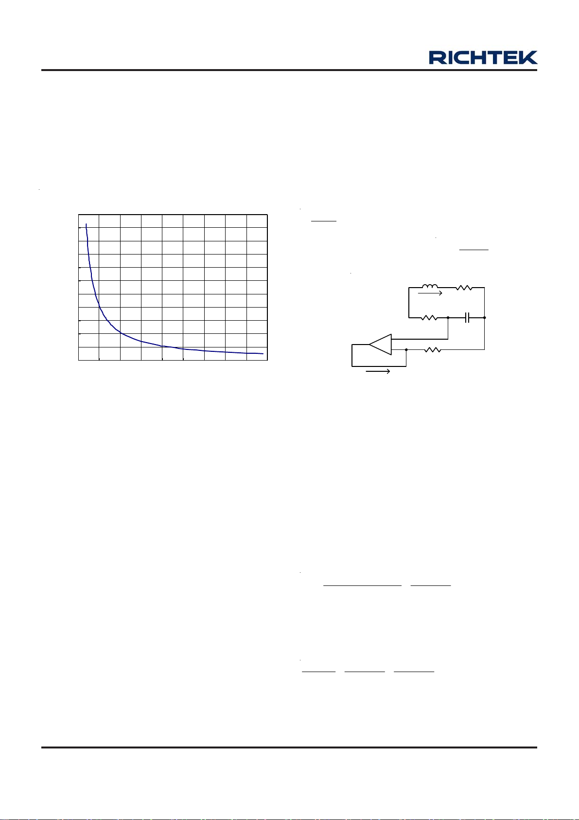
Operating Frequency Setting
The converter switching frequency is programmed by
simply connecting the resistor RRT between RT pin and
GND. Make sure the RRT is firmly connected between RT
pin and GND with a short trace length. If the RRT is removed,
there will not be any free running frequency. Figure 2
illustrates the switching frequency versus RRT.
Switching Frequency vs. R
1100
1000
900
800
700
600
500
400
300
200
Switching Frequency (kHz)
100
0
0 25 50 75 100 125 150 175 200 225
RRT (kٛ)
(kΩ)
RT
Figure 2. Switching Frequency vs. RT Resistance
R-C network is equal to the time constant of the inductor,
the voltage drop across the DCR is equal to the voltage
across the capacitor, namely V
DCR
= VC.
As shown in Figure 3, the differential GM amplifier converts
the voltage signal to a current signal IX for current balance
and output voltage droop control. The following equations
provide the calculation to determine the parameter values
of the current sensing network and R
L
If R C, than V = V = DCR I
The GM amplifier output current
=× ×
DCR
GMx
CDCR L
L
I
L
R
+
-
I
x
R
CSN
I =
X
.
CSN
V
C
R
CSN
DCR
+-
V
DCR
C
+-
V
C
Figure 3. DCR Current Sense Circuit
Control Loop
The RT8807/A is a two-phase voltage-mode PWM
controller. The control loop includes the power stage
(MOSFETs, inductors and output capacitors), the error
amplifier, the compensation network and the PWM
modulator. The converter's output voltage is sensed as
the feedback voltage through the divider resistors and then
fed into the negative input of the high-gain error amplifier.
The two-phase PWM signals are generated by the PWM
modulator, which compares the output voltage of the error
amplifier with two sawtooth waves, which are out of phase.
Therefore, the output voltage of the converter is determined
by the on-time duty ratio of the PWM signals. With proper
compensation, the feedback voltage can be regulated to
be equal to the reference voltage V
with required
REF
transient response.
Inductor Current Sense Setting
The DCR current sensing is a well-known lossless
technique to obtain a voltage signal which is proportional
to the inductor current. When the time constant of the
Dead Zone Elimination
When the converter is in the light load condition, the voltage
across the sensing capacitor, VC, will be negative. However,
the RT8807/A can not provide a negative IX and
consequently is not able to sense the negative inductor
current. This results in a dead zone in the load line
application. Therefore, a technique as shown in Figure 4
is utilized to eliminate the dead zone of the load line at
light load condition. Referring to Figure 4, IX can be
expressed as follows when voltage VC is negative.
(V I DCR)
I =
X
+×
OUT L
R R
CSN2 CSN
I DCR
×
L
+
To make sure that the RT8807/A can sense the inductor
current, the right hand side of the above equation should
always be positive :
V
OUT
R R R
CSN2 CSN2 CSN
I DCRI DCR
××
LL
++≥
0
12
DS8807/A-00 April 2008www.richtek.com
Page 13
RT8807/A
Since R
>> DCR in practical application, the above
CSN2
equation can be simplified as :
V
OUT
R R
CSN2 CSN
Therefore, R V
I DCR
×
L
≥
CSN2 OUT
R
≤×
CSN
I DCR
×
L
For example, assuming the negative inductor current is
equal to -5A at no load condition. For R
DCR = 1.7mΩ, V
R1.2
R55.06k
Choose R
≤×
CSN2
≤Ω
CSN2
CSN2
GMx
Ix
= 1.2V,
OUT
390
-5 1.7 10
××
= 54.9kΩ
+
-
R
CSN2
-3
L
I
L
R
R
CSN
DCR
+-
V
DCR
C
+-
V
C
CSN
V
OUT
= 390Ω,
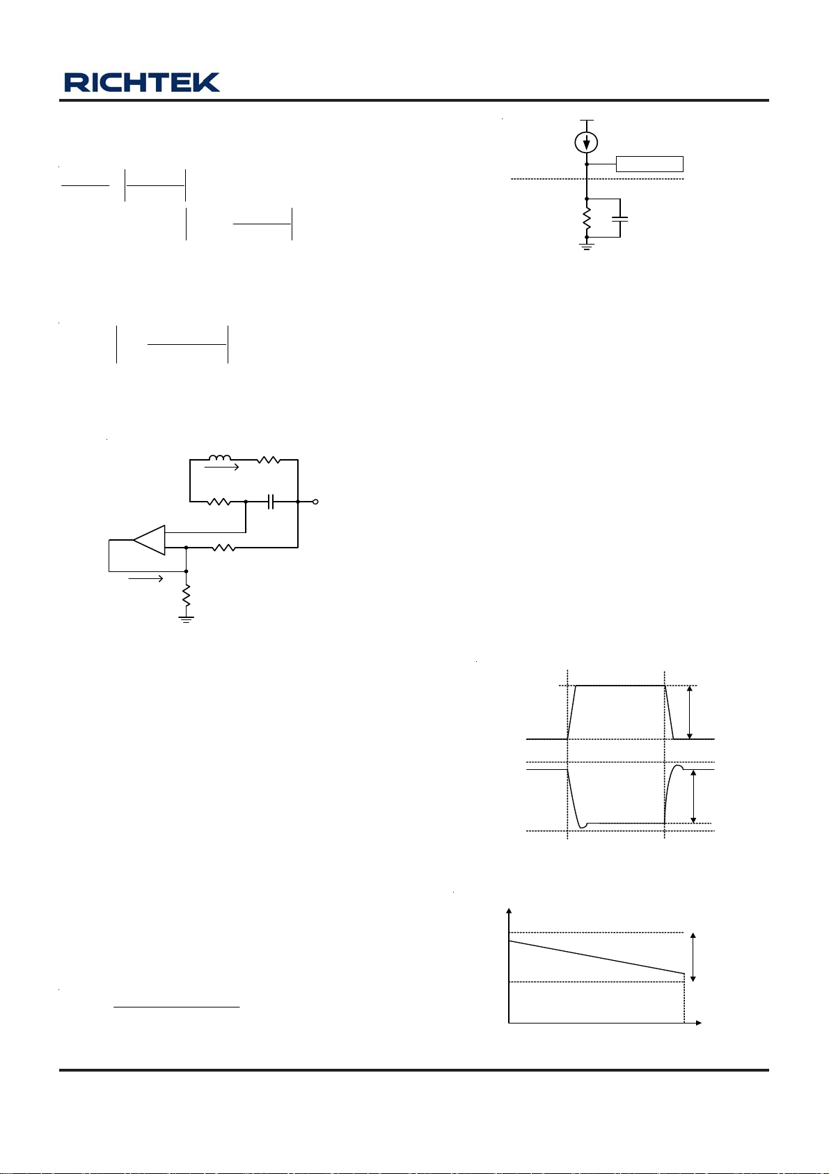
Figure 4. Application Circuit for Dead Zone Elimination
Sensed Output
Current
(I
+ IX2) x 2
X1
IOUT/IMAX
R
IMAX
OCP Circuit
Optional
Figure 5. Over Current Protection Function
Output Voltage Droop Control and Load Line
Setting
The RT8807/A supports the adaptive voltage droop control.
The concept of the output voltage droop control is to set
the output voltage level to be regulated slightly higher than
the minimum value at light load, and somewhat lower than
the maximum value at full load. As shown in Figure 6, a
larger downward voltage drop during step load is allowed,
which means the number of the required output capacitors
can be reduced or allows the use of capacitor with higher
ESR.
As a result, the full window of output voltage tolerance
can be used during the transient period (see Figure 7),
which reduces the overall cost. Another advantage of
output voltage droop control is that the output power of
the converter at full load is reduced, which greatly facilitates
the thermal design.
I
OUT
Over Current Protection Function
ΔI
?I
OUT
The over current threshold is determined by the resistor
OUT
connected to IOUT/IMAX pin. The two GM amplifier's
V
output currents are summed together and doubled, and
then flows out into the resistor R
, which is connected
IMAX
between IOUT/IMAX pin and the ground. As shown in
Figure 5, the RT8807/A uses an external resistor R
IMAX
to
OUT(max)
V
OUT(min)
V
OUT
With Droop
?V
ΔV
OUT
OUT
set a programmable over current trip point. Once the voltage
across the R
exceeds the threshold V
IMAX
, the OCP
OCP
Figure 6. Output Voltage with Droop
function will be triggered. The following equation provides
V
(V)
the calculation of the R
value for a given maximum
IMAX
inductor current. If necessary, a small ceramic capacitor
OUT
V
OUT(max)
is recommended to be paralleled with the resistor for noise
I
OUT
Window
Output Voltage Tolerance
(A)
filtering to obtain accurate over current protection.
VR
×
R
IMAX
=
OCP CSN
2 I DCR
××
LOAD(MAX)
V
OUT(min)
No Load Full Load
Figure 7. Load Line
DS8807/A-00 April 2008 www.richtek.com
13
Page 14
RT8807/A
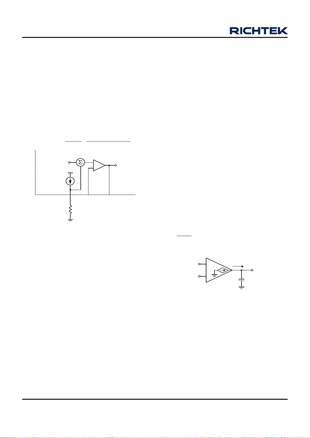
The two GM amplifier output currents (IX1 & IX2) are
internally summed and doubled, and then sent to DROOP
pin for droop setting. This current flows through the external
resistor R
, which is connected between DROOP and
DROOP
GND.
Therefore, the voltage across R
becomes load-
DROOP
current-dependent. As shown in Figure 8, the voltage
across R
is subtracted from the internal/external
DROOP
reference voltage and then sent to the positive input of the
error amplifier. Therefore, the load line slope can be
calculated using the following equation.
V2 DCRR
Δ××
Load line slope =
Internal/External
Reference
Sensed Output
Current
(I
+ IX2) x 2
X1
DROOP
R
DROOP
OUT DROOP
+
I R
Δ
OUT CSN
+
+
V
DROOP
-
-
+
EA
-
FB COMP
To PWM
Comparator
Figure 8. Output Voltage Droop Setting
Operating Phase Selection
The number of operating phase is designed to be selectable
to have more flexibility in different applications. EN2B pin
is used to select the number of operating phases.
After the initial turn-on of RT8807/A, an internal logic circuit
checks the voltage at EN2B pin. The threshold voltage of
dual-phase/single-phase operation is typically 1.15V. To
set RT8807/A as the dual-phase PWM controller, the
voltage at EN2B pin should be kept below 1.15V.
To set RT8807/A as a pure single-phase PWM controller,
connecting EN2B pin to a voltage that is higher than 1.15V
at power on. The RT8807/A then disables phase 2
(UGATE2 and LGATE2 are both held low) and operates as
a single-phase PWM controller.
In addition to the selectable number of operating phase,
the RT8807/A supports the operating phase transition.
Notice that if the controller is set to be in dual-phase
operation (voltage at EN2B pin is below the threshold),
further changing the voltage at EN2B pin to be higher than
the threshold will change the controller’s operating state
to single-phase operation. However, this operating phase
transition can only be carried out one time and is NOT
reversible. This means that once the controller changes
its operating state from dual-phase to single-phase, it can
not back to dual-phase operation no matter what the
voltage change is made at EN2B pin.
Besides, also notice that if the RT8807/A is set to be in
single-phase operation (voltage at EN2B pin is higher the
threshold), it can not be changed to operate in dual-phase
no matter what voltage change is made at EN2B pin. This
dual-phase to single-phase operation transition is
unidirectional.
Compensation Network Design
In order to have an accurate output voltage regulation with
fast transient response, an adequate compensator design
is necessary.
The RT8807/A uses a high-gain operational
transconductance amplifier (OTA) as the error amplifier.
As Figure 9 shows, the OTA works as the voltage
controlled current source because it takes the difference
of the two voltages as the input for current conversion.
I
Δ
GM = , where V = (V ) (V )
and V = I Z
OUT
V
Δ
M
ΔΔ×
COUTOUT
V
IN+
V
IN-
+
-
Δ−
MIN+IN-
I
GM
OUT
Z
OUT
V
C
Figure 9. Operational Transconductance Amplifier, OTA
The OTA output current flows through an impedance to
produce a voltage, which is referred to as the control
voltage. This control voltage is then fed to the PWM
modulator to compare with the sawtooth wave.
The first step of compensator design is to calculate the
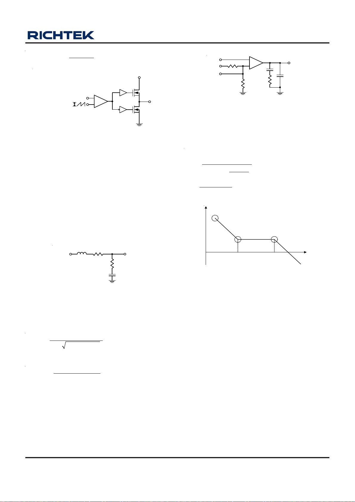
dc gain of the PWM modulator. Figure 10 shows the PWM
modulator, which is composed of the PWM comparator,
the drivers and both the high-side and low-side MOSFET.
The dc gain of the modulator is calculated by the input
voltage of the regulator, VIN, divided by the peak-to-peak
voltage of the oscillator, ΔV
OSC
.
14
DS8807/A-00 April 2008www.richtek.com
Page 15
V
OSC
V Δ
RAMP
IN
PWM
Comparator
+
C
-
Driver
Driver
V
IN
PHASE
Gain =
modulator
Error Amplifier Output, V
?V
Figure 10. PWM Modulator
As shown in Figure 11, the inductor and the output
capacitor together form a low-pass L-C output filter. The
input to the L-C output filter is the PHASE node and the
output is the regulator output. The ESR of the output
capacitor plays an important role in the compensator
design. The L-C filter introduces a double pole to the
system transfer function with a slope of -40dB/dec above
its corner frequency and a total phase lag of 180 degree.
The ESR of the output capacitor introduces a zero to the
system transfer function with a total phase shift of 90
degree.
RT8807/A
V
REF
V
OUT
R1
FB
Figure 12. Type II Compensator
Figure 13 shows the Bode diagram of the Type II
compensator. The frequencies of the single zero and the
two poles are determined as follows.
F = 0
P1
F =
P2
2R2
F =
Z1
2R2C2
π
π
1
××
()
1
××
F
P1
C1 C2
C1+C2
+
GM
-
C2
R2
R
F
C1
V
COMP
×
PHASE
DCR
ESR
C
Regulator
OUT
Output
L
OUT
Figure 11. Inductor and Output Capacitor
The second step is therefore to calculate the frequencies
of the pole and the zero. The frequency of the double pole
is determined as follows.
F =
P(LC)
2
π
1
××
LC
OUT OUT
The frequency of the zero is determined as follows.
F =
Z(ESR)
π
2C ESR
1
××
OUT
Note that the output capacitor(s) should have enough ESR
to satisfy the stability requirement.
The third step is to design the compensation network.
There are two kinds of compensation network: Type II and
Type III, both consist of the error amplifier and the
impedance network. Figure 12 shows the Type II
compensator.
F
Z1
F
P2
Figure 13. Gain Curve of Type II Compensator
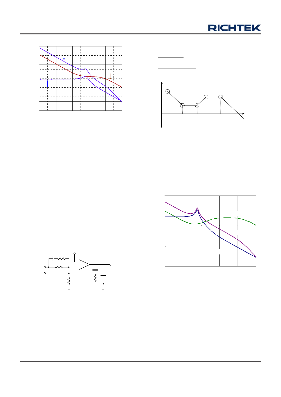
Figure 14 shows the Bode plot of the converter's gain vs.
frequency. The compensator helps to shape the profile of
the gain curve with respect to frequency. The zero gives a
90° boost to the phase to counteract the phase decay of
the double pole of the L-C filter. The first pole, FP1, gives a
shift to the gain curve in the low frequency range while the
second pole, FP2, provides further attenuation in the high
frequency range.
In general, a converter system control loop with high
bandwidth can achieve fast transient response but usually
tends to lose stability. Therefore, it is always a trade-off
between the control bandwidth and the system stability.
Empirically, FZ1 is placed at about 10% lower than the
double pole frequency of the L-C filter to have enough
phase margin. In general, the control bandwidth should
be higher than the frequency of the ESR zero but less
than 1/5 of the switching frequency. In addition, the F
P2
should be placed at half of the switching frequency.
DS8807/A-00 April 2008 www.richtek.com
15
Page 16
RT8807/A
80
80
Gain
Loop Gain
Frequency
Frequency (Hz)
Compensation
Gain
60
40
40
20
0
0
Modulator
Gain (d B)
-20
-40
-40
-60
-60
10Hz 100Hz 1.0KHz 10KHz 100KHz 1.0MHz
10 100 1k 10k 100k 1M
vdb(vo) vdb(comp2) vdb(lo)
Figure 14. Converter System Bode Plot with Type II
Compensator
For systems with low DCR and ESR parameters, the overall
efficiency can be higher and the output voltage ripple can
be lower. However, systems that have such L-C filters will
experience a very sharp slope downward in the phase
curve at the double pole and will be more difficult to
compensate. Compared to the Type II compensator, the
Type III compensator adds a pole-zero pair. The Type III
compensator utilizes two zeros to give a 180° phase boost,
and is usually used to compensate a converter with low
ESR output capacitors (e.g. OSCON or pure MLCC) to
provide the necessary phase margin for stability.
F =
P3
F =
Z1
F =
Z2
1
2R3C3
π
××
1
2R2C2
π
××
1
2 (R1+R3) C3
π
××
F
P1
F
Z1
F
F
Z2
F
P2
P3
Figure 16. Gain Curve of Type III Compensator
Figure 17 shows the Bode diagram of the converter's gain
vs. frequency with Type III compensator. It is recommended
that FZ1 is placed at half of the L-C double pole, FZ2 is
placed at the LC double pole, FP1 is placed at the ESR
zero and FP2 is placed at half of the switching frequency.
Loop Gain
60
40
20
Compensation Gain
Figure 15 shows the Type III compensator, which
introduces an extra pole-zero pair by inserting a series R-
C circuit between the V
C3
R3
V
OUT
FB
R1
node and the FB node.
OUT
V
REF
+
GM
-
C2
R
F
R2
C1
V
COMP
Figure 15. Type III Compensator
Figure 16 shows the Bode diagram of the Type III
compensator. The frequencies of the three poles and two
zeros are determined as follows.
F = 0
P1
F =
P2
2R2
π
1
C1 C2
××
×
()
C1+C2
0
dB
-20
-40
Modulator Gain
-60
-80
234567
Gain
Log Frequency
Figure 18. Converter System Bode Plot with Type III
Compensator
Over Temperature Protection
The operating temperature within the chip is continuously
monitored. The chip will be shut down when OTP occurs
with a typical trip point of 160°C.
16
DS8807/A-00 April 2008www.richtek.com
Page 17

RT8807/A
Power Stages
One of the most important concerns in designing a multi-
phase converter is to determine the number of phases.
Determining the number of phases highly depends on the
overall cost, the system constraints, and usually differs
case by case. The main concerns for the circuit designer
include the total available board space, the type of
component that can be used (through-hole/surface mount
device), the maximum load current, and of the most
importance, total cost. In general, the most economical
solutions are those in which each phase handles a current
ranging from 20A to 25A (using one high-side MOSFET
and one low-side MOSFET). Design with all surface mount
devices will tend toward to the lower end of this current
range due to the power dissipation capability. If the power
device in through-hole type is available, higher current
per phase is possible. In cases where the board area is
the design limitation, the current per phase can be pushed
up to 40A. However, these designs require appropriate
heat sinks and forced air cooling to remove the large
amount of heat, which is generated by the power
MOSFETs, the inductors and the PCB copper traces.
MOSFET Selection
The majority of power loss in the step-down power
conversion is due to the loss in the power MOSFETs. In
the low-voltage high-current applications, the duty cycle
of the high-side MOSFET is small. Therefore, the switching
loss of the high-side MOSFET is of concern. Power
MOSFETs with lower total gate charge are preferred in
choosing the high-side power devices.
However, the small duty cycle means the low-side
MOSFET is on for most of the switching cycle. Therefore,
the conduction loss tends to dominate the total power
loss of the converter. To improve the overall efficiency, the
MOSFETs with low R
are preferred in the circuit
DS(ON)
design. In some cases, more than one MOSFET are
connected in parallel to further decrease the on-state
resistance. However, this depends on the low-side
MOSFET driver capability and the budget.
Package Power dissipation
It is also important to consider the amount of power being
dissipated in the two embedded MOSFET drivers when
choosing power switches. Since there are two drives in
the same package, the total power dissipation must not
exceed the maximum allowable power dissipation for the
VQFN package. Calculating the power dissipation in the
drivers is crucial to ensure a safe operation of the controller.
Exceeding the maximum allowable power dissipation will
let the IC to be operated beyond the recommended
maximum junction temperature of 125°C.
The maximum power dissipation for the 4x4 V/WQFN
package is approximately equal to 1.923W at room
temperature. The following equations provide the integrated
drivers' power dissipation estimation.
PD = (C
UGATE
x V
BOOT − PHASE2
x fSW) + (C
LGATE
x V
CC
2
x
fSW)
TJ = TA + (θJA x PD)
where the C
UGATE
and the C
represent the C
LGATE
ISS
of the
high-side MOSFET and the low-side MOSFET,
respectively. From the above equations, it is clear that
the junction temperature is directly proportional to the
total C
For instance, if C
in parallel), V
frequency f
of all the external MOSFETs.
ISS
= 1nF, C
UGATE
BOOT−PHASE
= 300kHz, the power dissipation in the driver
sw
= 5V, V
= 5nF (two MOSFETs
LGATE
= 12V, switching
CC
per phase can be obtained :
≈
PD 1n x 52 x 300k + 2 x 5n x 122 x 300k = 439mW
Assuming the room temperature is equal to 30°C, the
junction temperature for two-phase operation is :
TJ = 30°C + (52°C/W) x (0.439W x 2) = 75.6°C < 125°C,
which means the junction temperature is below the
maximum recommended value for a safe operation.
Layout Considerations
Layout plays a critical role in modern high-frequency
switching converter design. Circuit board with careful
layout can help the IC function properly and achieve low
losses, low switching noise, and stable operation with
improved performance. Without a carefully layout, the PCB
could radiate excessive noise, causing noise-induced IC
problems and then contribute to the converter instability.
The following guidelines can be used to achieve optimal
IC performance.
DS8807/A-00 April 2008 www.richtek.com
17
Page 18

RT8807/A
1. Power components should be placed first. Place the
input capacitors close to the power MOSFETs, then
locate the filter inductors and output capacitors between
the power MOSFETs and the load.
2. Place both the ceramic and bulk input capacitor close
to the drain pin of the high-side MOSFET. This can
reduce the impedance presented by the input bulk
capacitance at high switching frequency. If there is more
than one high-side MOSFET in parallel, each should
have its own individual ceramic capacitor.
3. Keep the power loops as short as possible. For low-
voltage high-current applications, power components
are the most critical part in the layout because they
switch a large amount of current. The current transition
from one device to another at high speed causes voltage
spikes due to the parasitic components on the circuit
board. Therefore, all of the high-current switching loops
should be kept as short as possible with large and thick
copper traces to minimize the radiation of
electromagnetic interference.
setting components and any bypass capacitors. These
components belong to the high-impedance circuit loop
and are inherently sensitive to noise pick-up. Therefore,
they must be located close to their respective controller
pins and away from the noisy switching nodes.
9. A multi-layer PCB design is recommended. Make use
of one single layer as the power ground and have a
separate control signal ground as the reference of all
signals.
4. Minimize the trace length between the power MOSFETs
and its drivers.
Since the drivers use short, high-current pulses to drive
the power MOSFETs, the driving traces should be sized
as short and large as possible to reduce the trace
inductance. This is especially true for the low-side
MOSFET, since this can reduce the possibility of the
shoot-through.
5. Provide enough copper area around the power
MOSFETs and the inductors to aid in heat sinking.
Use thick copper PCB to reduce the resistance and
inductance for improved efficiency.
6. The bank of output capacitor should be placed physically
close to the load. This can minimize the impedance
seen by the load, and then improves the transient
response.
7. Place all of the high-frequency decoupling ceramic
capacitors close to their decoupling targets.
8. Small signal components should be located as close
as possible to the IC. The small signal components
include the feedback components, current sensing
components, the compensation components, function
18
DS8807/A-00 April 2008www.richtek.com
Page 19
Outline Dimension
RT8807/A
D
E
A
A3
A1
D2
SEE DETAIL A
L
1
E2
1
2
be
DETAIL A
Pin #1 ID and Tie Bar Mark Options
Note : The configuration of the Pin #1 identifier is optional,
1
2
but must be located within the zone indicated.
Dimensions In Millimeters Dimensions In Inches
Symbol
Min Max Min Max
A 0.800 1.000 0.031 0.039
A1 0.000 0.050 0.000 0.002
A3 0.175 0.250 0.007 0.010
b 0.180 0.300 0.007 0.012
D 3.950 4.050 0.156 0.159
D2 2.300 2.750 0.091 0.108
E 3.950 4.050 0.156 0.159
E2 2.300 2.750 0.091 0.108
e 0.500 0.020
L 0.350 0.450
0.014 0.018
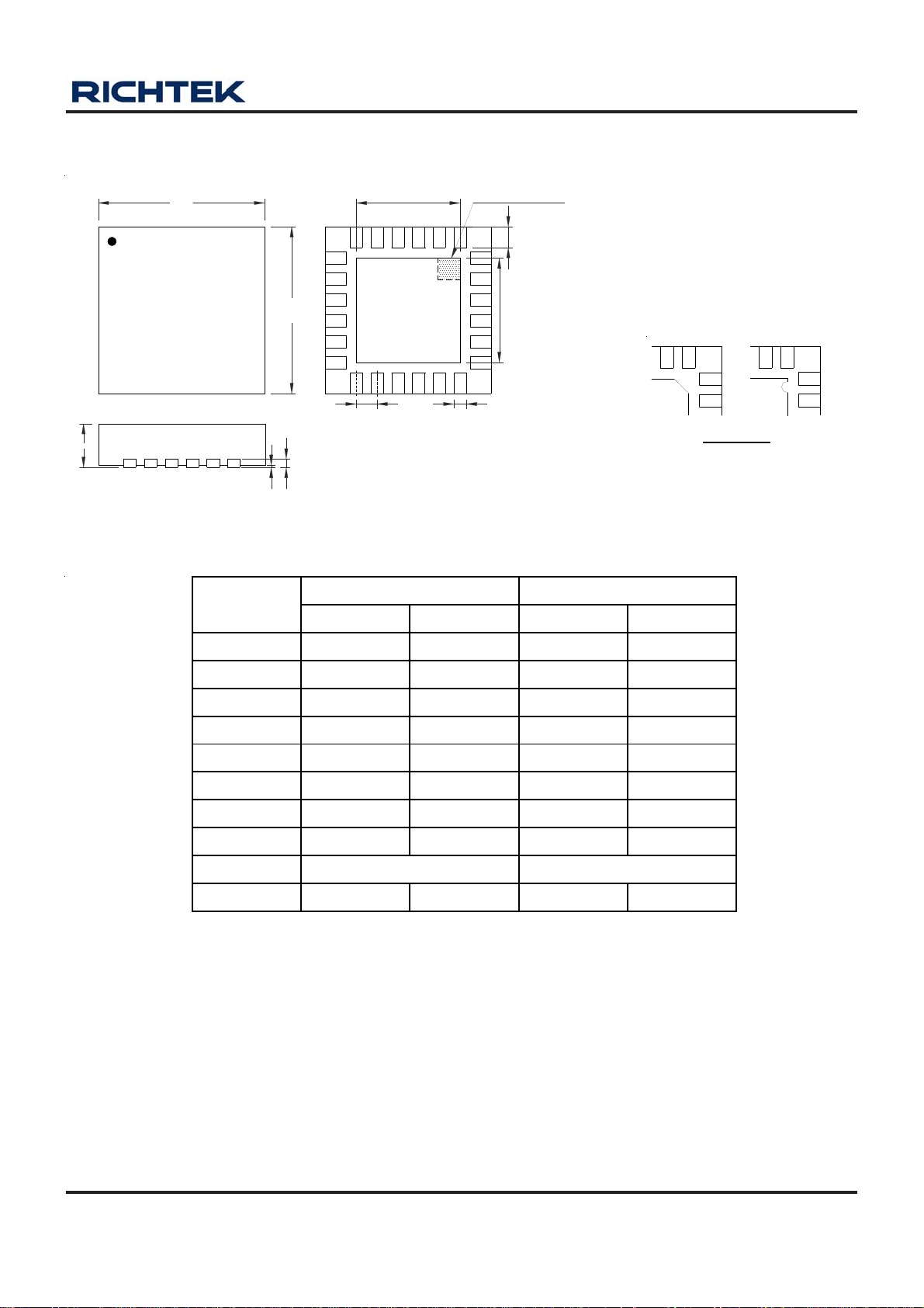
V-Type 24L QFN 4x4 Package
DS8807/A-00 April 2008 www.richtek.com
19
Page 20
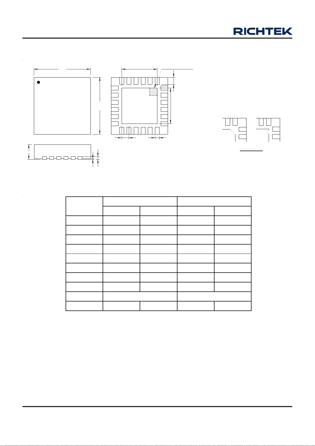
RT8807/A
D
E
A
A3
A1
D2
SEE DETAIL A
L
1
E2
1
2
be
DETAIL A
Pin #1 ID and Tie Bar Mark Options
Note : The configuration of the Pin #1 identifier is optional,
1
2
but must be located within the zone indicated.
Dimensions In Millimeters Dimensions In Inches
Symbol
Min Max Min Max
A 0.700 0.800 0.028 0.031
A1 0.000 0.050 0.000 0.002
A3 0.175 0.250 0.007 0.010
b 0.180 0.300 0.007 0.012
D 3.950 4.050 0.156 0.159
D2 2.300 2.750 0.091 0.108
E 3.950 4.050 0.156 0.159
E2 2.300 2.750 0.091 0.108
e 0.500 0.020
L 0.350 0.450
Richtek Technology Corporation
Headquarter
5F, No. 20, Taiyuen Street, Chupei City
Hsinchu, Taiwan, R.O.C.
Tel: (8863)5526789 Fax: (8863)5526611
0.014 0.018
W-Type 24L QFN 4x4 Package
Richtek Technology Corporation
Taipei Office (Marketing)
8F, No. 137, Lane 235, Paochiao Road, Hsintien City
Taipei County, Taiwan, R.O.C.
Tel: (8862)89191466 Fax: (8862)89191465
Email: [email protected]
20
DS8807/A-00 April 2008www.richtek.com
 Loading...