

Page 1
RT8803A
2/3-Phase PWM Controller for High-Density Power Supply
General Description
The RT8803A is a 2/3-phase synchronous buck controller
specifically designed to power Intel
®
/ AMD next generation
microprocessors. It implements an internal 8-bit DAC that is
identified by VID code of microprocessor directly. R T8803A
generates VID table that conform to Intel® VRD10.x and
VRD11 core power with 6.25mV increments and 0.5%
accura cy.
RT8803A adopts innovative time-sharing DCR current sensing
technique to sense pha se currents for phase current bala nce,
load line setting and over current protection. Using a common
GM to sense all pha se currents eliminates offset and line arity
variation between GMs in conventional current sensing
methods. As sub-milli-ohm-grade inductors are widely used
in modern motherboards, slight offset and linearity mismatch
will cause considerable current shift between pha ses. This
technique ensures good current balance at ma ss production.
Other features include over current protection, programma ble
soft start, over voltage protection, and output off set setting.
RT8803A comes to a small footprint package with
VQF N-32L 5x5.
Ordering Information
RT8803A
Features
zz
5V Power Supply
z
zz
zz
z 2/3-Phase Power Conversion with Automatic Phase
zz
Selection
zz
z 8-bit VID Interface, Supporting Intel VR D11/V RD10.x
zz
and AMD K8, K8_M2 CPUs
zz
z VR_HOT and VR_FAN Indication
zz
zz
z Precision Core Voltage Regulation
zz
zz
z Power Stage Thermal Balance by DCR Current
zz
Sensing
zz
z Adjustable Soft-start
zz
zz
z Over-Voltage Protection
zz
zz
z Adjustable Frequency and Typical at 300kHz per
zz
Phase
zz
z Power Good Indication
zz
zz
z 32-Lead VQFN Package
zz
zz
z RoHS Compliant and 100% Lead (Pb)-Free
zz
Applications
®
z Intel
z Low Output Voltage, High power density DC-DC
z V oltage Regulator Modules
/AMD New generation microprocessor for Desktop
PC and Motherboard
Converters
Package Type
QV : VQFN-32L 5x5 (V-Type)
Operating Temperature Range
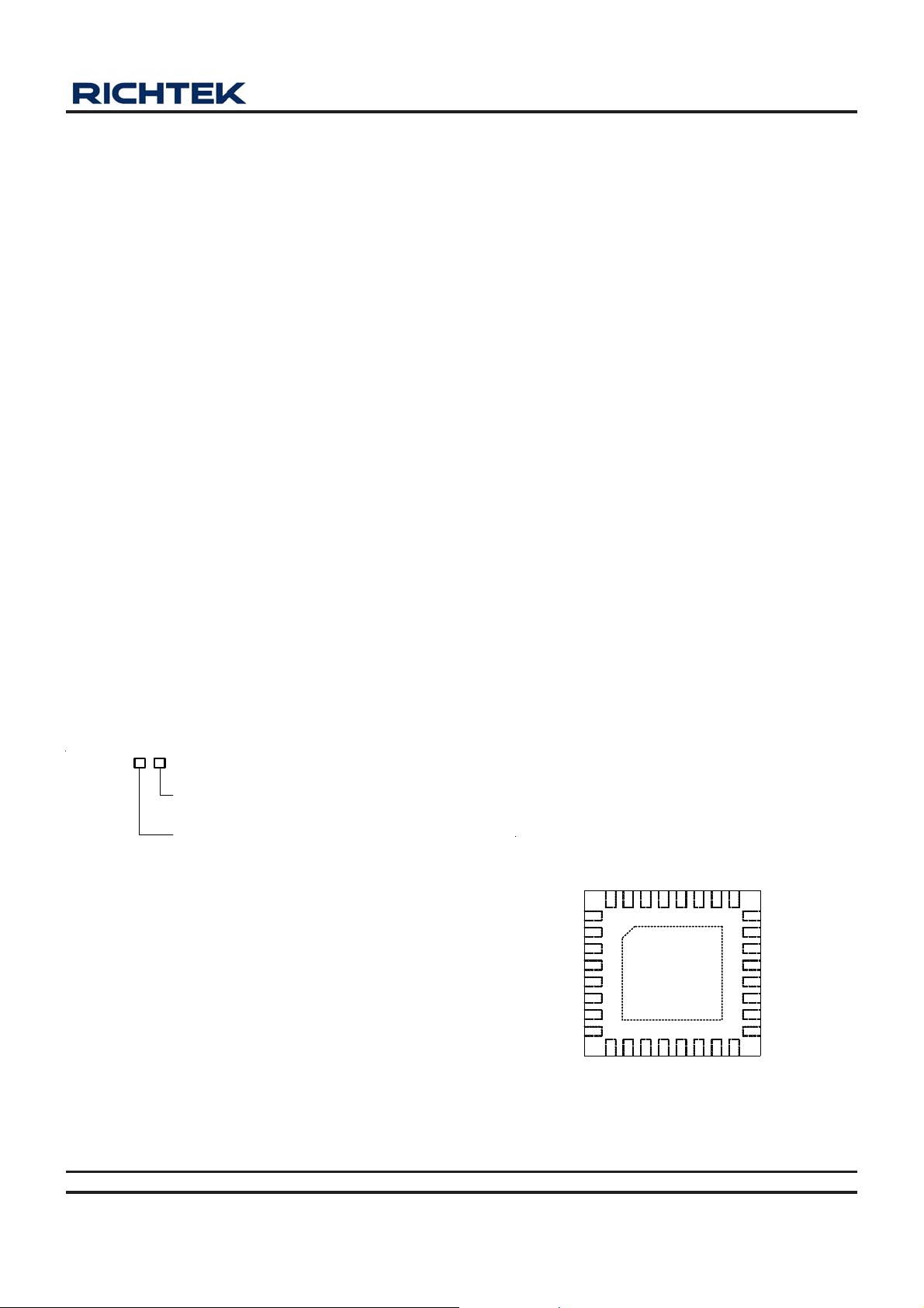
Pin Configurations
(TOP VIEW)
P : Pb Free with Commercial Standard
G : Green (Halogen Free with Commer-
VID_SEL
VID0
VID1
VID2
VID3
VID4
VID5
IMAX
VID6
24
VID7
23
VDD
22
PWM3
21
PWM2
20
PWM1
19
ISP1
18
33
ISP2
17
ISP3
1615
ISN1
ISN23
cial Standard)
Note :
Richtek Pb-free and Green products are :
`RoHS compliant and compatible with the current require ments of IPC/JEDEC J-STD-020.
`Suitable for use in SnPb or Pb-free soldering processes.
`100% matte tin (Sn) plating.
VTT/EN
VR_Ready
FBRTN
FB
COMP
SS
VR_FAN
VR_HOT
32 31 30 29
1
2
3
4
5
6
7
8
9101112 1413
DVD
TSEN
RT
GND
OFS
28 27 26 25
ADJ
VQFN-32L 5x5
All brandname or trademark belong to their owner respectively
DS8803A-05 August 2007 www.richtek.com
1
Page 2
RT8803A
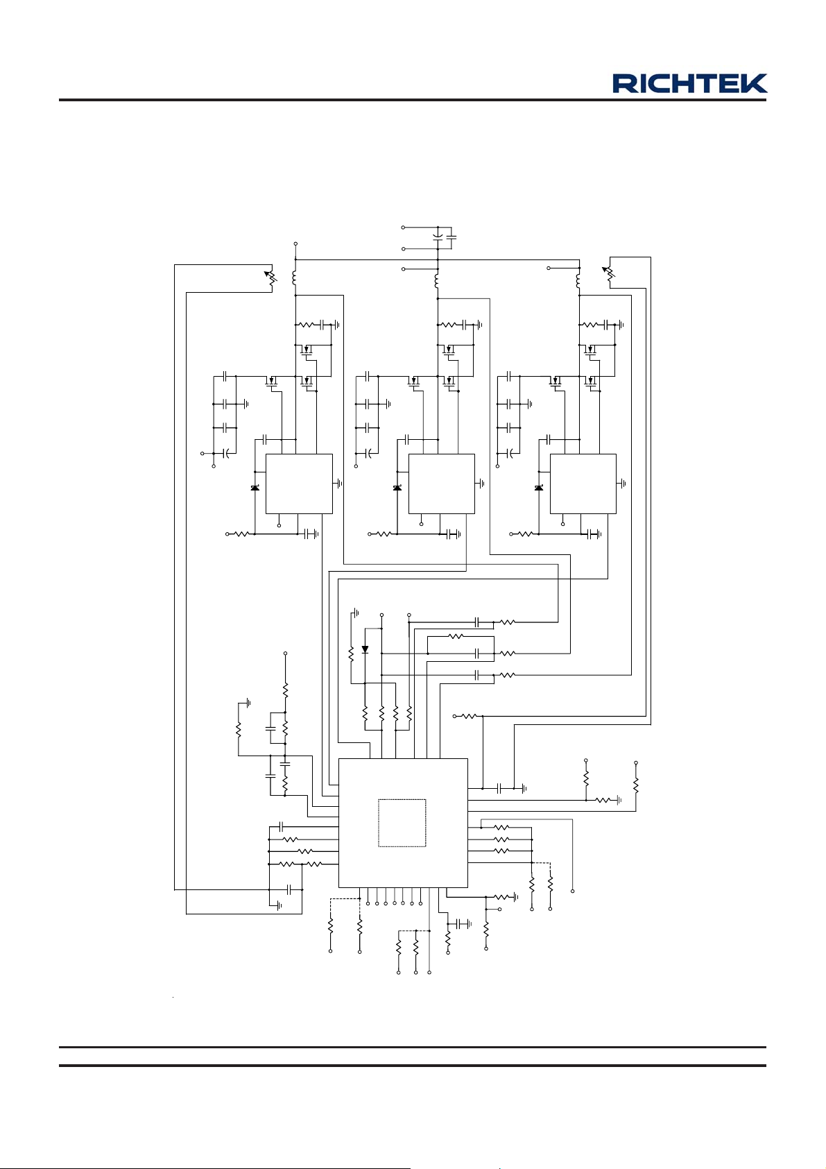
Typical Application Circuit
1
CORE
V
2k
L1
RT2
NTC
280nH
C17
3.3nF
2.2
R28
Q3
C15
4.7uF
Q1
Q2
4.7uF
IPD09N03LA
4.7uF
1uF
C16
C12 C13 C14
1200uF
IN
V
BTX_12V
BTX_12V
R27
8
1
BOOT
1N4148
NC
3
10
IPS06N03LA
7
5
LGATE
PHASE
UGATE
4
6
PGND
RT9619
VCC
PWM
2
C11
0.1uF
SS
V
CC
V
23
CORE
V
C22
4.7uF
4.7uF
C20 C21
4.7uF
C19
1200uF
IN
V
1N4148
R29
10
BTX_12V
23
CORE
V
C23
1
1uF
1
CORE
V
Q4
BOOT
3
560uF x 10
C42 to C59
C32 to C41
10uF x 18
23
L2
280nH
C24
3.3nF
2.2
R30
Q6
Q5
IPD09N03LA
IPS06N03LA
8
7
5
LGATE
PHASE
UGATE
RT9619
NC
VCC
4
C18
0.1uF
IN
V
6
PGND
VIN
2
1uF
C10
CORE
V
4.7uF
Q7
4.7uF
4.7uF
C30
1uF
C26 C27 C28 C29
1200uF
BTX_12V
8
1
BOOT
1N4148
NC
3
R31
10
NTC
10k
L3
RT1
280nH
3.3nF
C31
2.2
R32
Q9
Q8
IPD09N03LA
IPS06N03LA
7
5
LGATE
PHASE
UGATE
6
PGND
RT9619
VCC
VIN
4
2
C25
0.1uF
R33
CPU_VCC
0
R17
C7
R16
1.5k
470pF
C6
R14
R13
5.6pF
2.2nF
15k
R15
C4
56nF
8.2k
12k
300
R11
C3
56nF
C5
R12
300
For AMD
BTX_5V
PWM2
PWM1
FB
542021
COMP
6
SS
14
IMAX
11
RT
13
ADJ
100
R19
R18
For Intel
75k
360
75k
VID_SEL
32293031282526
VID_SEL
360
R22
R20
R21
22
16
15
ISN1
ISN23
PWM3
GND
RT8803A
VID0
VID1
VID2
VID3
VID4
27
VID0
VID1
VID2
VID3
VID4
For K8
VDDIO
191817
ISP1
VID5
VID5
For K8_M2
VID6
VID6
GND
ISP2
ISP3
FBRTN
VR_Ready
VR_FAN
VR_HOT
VTT/EN
VID7
VDD
232410
10
R1
VID7
R25
TSEN
OFS
DVD
BTX_5V
NC
360 360 360
R23 R24 R26
C8 C92
1uF 1uF
R7
BTX_5V
BTX_5V
R8
91872 12
C2
0.1uF
3
R6
R5
R4
R3
1.1k
For Intel
C1
0.1uF
Enable
10k
R2
BTX_12V
VTT
NC
10k
10k
10k
For AMD
PGOOD
VDDIO
CPU_VSS
0
R9
R10
NC
All brandname or trademark belong to their owner respectively
DS8803A-05 August 2007www.richtek.com
2
Page 3

Functional Pin Description
VTT/EN (Pin 1)
The pin is defined as the chip enable, and the VTT is
applied f or internal VID pull high power a nd power sequence
monitoring.
VR_Ready (Pin 2)
Power good open-drain output.
FBRT N (Pin 3)
Feedback return pin. VID DAC and error a mplifier reference
for remote sensing of the output voltage.
FB (Pin 4)
Inverting input pin of the internal error a mplifier .
COMP (Pin 5)
Output pin of the error amplifier a nd input pin of the PWM
comparator.
SS (Pin 6)
Connect this SS pin to GND with a capacitor to set the
soft-start time interval.
VR_F AN (Pin 7)
The pin is defined to signal VR thermal information for
external VR thermal dissipation scheme triggering.
RT8803A
OFS (Pin 12)
The pin is defined for load line offset setting.
ADJ (Pin 13)
Current sense output for active droop a djusting. Connect
a resistor from this pin to GN D to set the load droop.
IMAX (Pin 14)
The pin is defined to set threshold of over current.
ISN1 (Pin 15)
Current sense negative input pin for channel 1 current
sensing.
ISN23 (Pin 16)
Current sense negative input pins for channel 2 and
channel 4 current sensing.
ISP1 (Pin 19), ISP2 (Pin 18), ISP3 (Pin 17)
Current sense positive input pins for individual converter
channel current sensing.
PWM1 (Pin 20), PWM2 (Pin 21), PWM3 (Pin 22)
PWM outputs for ea ch driven channel. Connect these pins
to the PWM input of the MOSFET driver. For systems
which using 2/3/4 channels, pull PWM 3/4/5 pins up to
high.
VR_HOT (Pin 8)
The pin is defined to signal VR thermal information for
external VR thermal dissipation scheme triggering.
TSEN (Pin 9)
T emperature detect pin f or VR_HOT a nd VR_F AN.
D V D (Pin 10)
Programma ble power UVLO detection input. Tri p threshold
is 1V at V
RT (Pin 11)
The pin is defined to set internal switching operation
frequency . Connect this pin to GN D with a resistor RRT to
set the frequency FSW.
F
SW
DS8803A-05 August 2007 www.richtek.com
rising.
DVD
9
RT
e 4.463
3500R
+
All brandname or trademark belong to their owner respectively
=
V DD (Pin 23)
IC power supply . Conne ct this pin to a 5V supply.
VID7 (Pin 24), VID6 (Pin 25), VID5 (Pin 26), VID4 (Pin
27), VID3 (Pin 28), VID2 (Pin 29), VID1 (Pin 30),
VID0 (Pin 31), VID_SEL (32)
DAC voltage identification inputs for V RD10.x / VRD11 /
K8 / K8_M2 . These pins are internally pulled up to VTT.
VIDSEL VID [7] Table
VTT X VR11
GND X VR10.x
VDD NC K8
VDD GND K8_M2
GND [Exposed pad (33)]
The exposed pad must be soldered to a large PCB and
connected to GND f or maximum power dissi pation.
3
Page 4
RT8803A
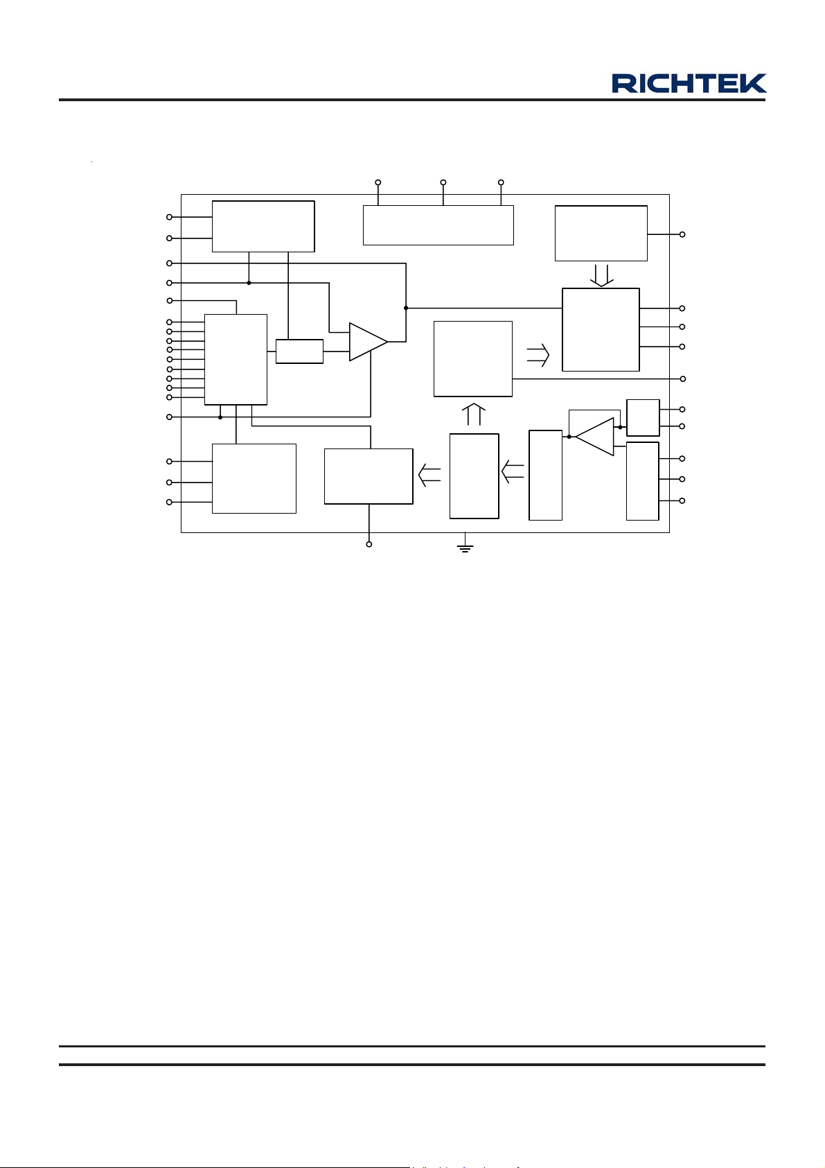
Function Block Diagram
DVDVTT/ENVDD
SS
VR_Ready
COMP
FB
OFS
VID7
VID6
VID5
VID4
VID3
VID2
VID1
VID0
VID_SEL
FBRTN
TSEN
VR_FAN
VR_HOT
Soft Start
& PGOOD
DAC
Temperature
Processing
Clamp
-
EA
+
Droop Tune
& Hi-I
Detection
ADJ
Power On
Reset
Processing
Detection
Current
SUM/N
& OCP
Sample
& Hold
GND
Mux
Oscillator
&
Ramp
Generator
Pulse
Width
Modulator
& Output
Buffer
-
CSA
+
Mux
Mux
RT
PWM1
PWM2
PWM3
IMAX
ISN1
ISN23
ISP1
ISP2
ISP3
All brandname or trademark belong to their owner respectively
DS8803A-05 August 2007www.richtek.com
4
Page 5
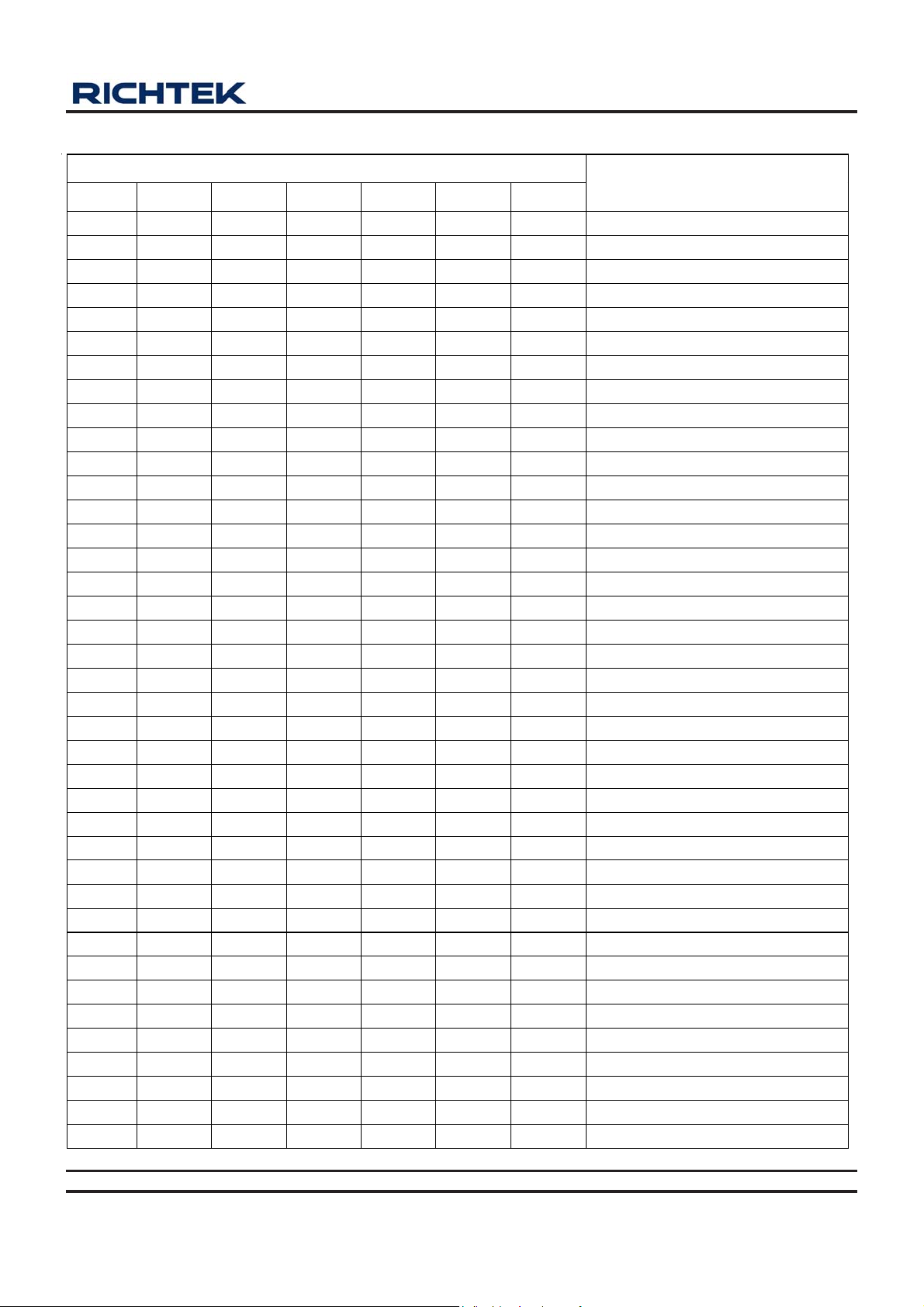
Table 1. Output Voltage Program (VRD10.x + VID6)
RT8803A
Pin Name
VID4 VID3 VID2 VID1 VID0 VID5 VID6
0 1 0 1 0 1 1 1.60000V
0 1 0 1 0 1 0 1.59375V
0 1 0 1 1 0 1 1.58750V
0 1 0 1 1 0 0 1.58125V
0 1 0 1 1 1 1 1.57500V
0 1 0 1 1 1 0 1.56875V
0 1 1 0 0 0 1 1.56250V
0 1 1 0 0 0 0 1.55625V
0 1 1 0 0 1 1 1.55000V
0 1 1 0 0 1 0 1.54375V
0 1 1 0 1 0 1 1.53750V
0 1 1 0 1 0 0 1.53125V
0 1 1 0 1 1 1 1.52500V
0 1 1 0 1 1 0 1.51875V
0 1 1 1 0 0 1 1.51250V
0 1 1 1 0 0 0 1.50625V
0 1 1 1 0 1 1 1.50000V
0 1 1 1 0 1 0 1.49375V
0 1 1 1 1 0 1 1.48750V
0 1 1 1 1 0 0 1.48125V
0 1 1 1 1 1 1 1.47500V
0 1 1 1 1 1 0 1.46875V
1 0 0 0 0 0 1 1.46250V
1 0 0 0 0 0 0 1.45625V
1 0 0 0 0 1 1 1.45000V
1 0 0 0 0 1 0 1.44375V
1 0 0 0 1 0 1 1.43750V
1 0 0 0 1 0 0 1.43125V
1 0 0 0 1 1 1 1.42500V
1 0 0 0 1 1 0 1.41875V
1 0 0 1 0 0 1 1.41250V
1 0 0 1 0 0 0 1.40625V
1 0 0 1 0 1 1 1.40000V
1 0 0 1 0 1 0 1.39375V
1 0 0 1 1 0 1 1.38750V
1 0 0 1 1 0 0 1.38125V
1 0 0 1 1 1 1 1.37500V
1 0 0 1 1 1 0 1.36875V
1 0 1 0 0 0 1 1.36250V
All brandname or trademark belong to their owner respectively
DS8803A-05 August 2007 www.richtek.com
Nominal Output Voltage DACOUT
To be continued
5
Page 6
RT8803A
Table 1. Output Voltage Program (VRD10.x + VID6)
Pin Name
Nominal Output Voltage DACOUT
VID4 VID3 VID2 VID1 VID0 VID5 VID6
1 0 1 0 0 0 0 1.35625V
1 0 1 0 0 1 1 1.35000V
1 0 1 0 0 1 0 1.34375V
1 0 1 0 1 0 1 1.33750V
1 0 1 0 1 0 0 1.33125V
1 0 1 0 1 1 1 1.32500V
1 0 1 0 1 1 0 1.31875V
1 0 1 1 0 0 1 1.31250V
1 0 1 1 0 0 0 1.30625V
1 0 1 1 0 1 1 1.30000V
1 0 1 1 0 1 0 1.29375V
1 0 1 1 1 0 1 1.28750V
1 0 1 1 1 0 0 1.28125V
1 0 1 1 1 1 1 1.27500V
1 0 1 1 1 1 0 1.26875V
1 1 0 0 0 0 1 1.26250V
1 1 0 0 0 0 0 1.25625V
1 1 0 0 0 1 1 1.25000V
1 1 0 0 0 1 0 1.24375V
1 1 0 0 1 0 1 1.23750V
1 1 0 0 1 0 0 1.23125V
1 1 0 0 1 1 1 1.22500V
1 1 0 0 1 1 0 1.21875V
1 1 0 1 0 0 1 1.21250V
1 1 0 1 0 0 0 1.20625V
1 1 0 1 0 1 1 1.20000V
1 1 0 1 0 1 0 1.19375V
1 1 0 1 1 0 1 1.18750V
1 1 0 1 1 0 0 1.18125V
1 1 0 1 1 1 1 1.17500V
1 1 0 1 1 1 0 1.16875V
1 1 1 0 0 0 1 1.16250V
1 1 1 0 0 0 0 1,15625V
1 1 1 0 0 1 1 1.15000V
1 1 1 0 0 1 0 1.14375V
1 1 1 0 1 0 1 1.13750V
1 1 1 0 1 0 0 1.13125V
1 1 1 0 1 1 1 1.12500V
1 1 1 0 1 1 0 1.11875V
All brandname or trademark belong to their owner respectively
DS8803A-05 August 2007www.richtek.com
6
To be continued
Page 7
Table 1. Output Voltage Program (VRD10.x + VID6)
RT8803A
Pin Name
VID4 VID3 VID2 VID1 VID0 VID5 VID6
1 1 1 1 0 0 1 1.11250V
1 1 1 1 0 0 0 1.10625V
1 1 1 1 0 1 1 1.10000V
1 1 1 1 0 1 0 1.09375V
1 1 1 1 1 0 1 OFF
1 1 1 1 1 0 0 OFF
1 1 1 1 1 1 1 OFF
1 1 1 1 1 1 0 OFF
0 0 0 0 0 0 1 1.08750V
0 0 0 0 0 0 0 1.08125V
0 0 0 0 0 1 1 1.07500V
0 0 0 0 0 1 0 1.06875V
0 0 0 0 1 0 1 1.06250V
0 0 0 0 1 0 0 1.05625V
0 0 0 0 1 1 1 1.05000V
0 0 0 0 1 1 0 1.04375V
0 0 0 1 0 0 1 1.03750V
0 0 0 1 0 0 0 1.03125V
0 0 0 1 0 1 1 1.02500V
0 0 0 1 0 1 0 1.01875V
0 0 0 1 1 0 1 1.01250V
0 0 0 1 1 0 0 1.00625V
0 0 0 1 1 1 1 1.00000V
0 0 0 1 1 1 0 0.99375V
0 0 1 0 0 0 1 0.98750V
0 0 1 0 0 0 0 0.98125V
0 0 1 0 0 1 1 0.97500V
0 0 1 0 0 1 0 0.96875V
0 0 1 0 1 0 1 0.96250V
0 0 1 0 1 0 0 0.95625V
0 0 1 0 1 1 1 0.95000V
0 0 1 0 1 1 0 0.94375V
0 0 1 1 0 0 1 0.93750V
0 0 1 1 0 0 0 0.93125V
0 0 1 1 0 1 1 0.92500V
0 0 1 1 0 1 0 0.91875V
0 0 1 1 1 0 1 0.91250V
0 0 1 1 1 0 0 0.90625V
0 0 1 1 1 1 1 0.90000V
All brandname or trademark belong to their owner respectively
DS8803A-05 August 2007 www.richtek.com
Nominal Output Voltage DACOUT
To be continued
7
Page 8
RT8803A
Table 1. Output Voltage Program (VRD10.x + VID6)
Pin Name
VID4 VID3 VID2 VID1 VID0 VID5 VID6
0 0 1 1 1 1 0 0.89375V
0 1 0 0 0 0 1 0.88750V
0 1 0 0 0 0 0 0.88125V
0 1 0 0 0 1 1 0.87500V
0 1 0 0 0 1 0 0.86875V
0 1 0 0 1 0 1 0.86250V
0 1 0 0 1 0 0 0.85625V
0 1 0 0 1 1 1 0.85000V
0 1 0 0 1 1 0 0.84375V
0 1 0 1 0 0 1 0.83750V
0 1 0 1 0 0 0 0.83125V
Nominal Output Voltage DACOUT
All brandname or trademark belong to their owner respectively
DS8803A-05 August 2007www.richtek.com
8
Page 9
Table 2. Output Voltage Program (VRD11)
RT8803A
Pin Name
Nominal Output Voltage DACOUT
HEX
00 OFF
01 OFF
02 1.60000V
03 1.59375V
04 1.58750V
05 1.58125V
06 1.57500V
07 1.56875V
08 1.56250V
09 1.55625V
0A 1.55000V
0B 1.54375V
0C 1.53750V
0D 1.53125V
0E 1.52500V
0F 1.51875V
10 1.51250V
11 1.50625V
12 1.50000V
13 1.49375V
14 1.48750V
15 1.48125V
16 1.47500V
17 1.46875V
18 1.46250V
19 1.45625V
1A 1.45000V
1B 1.44375V
1C 1.43750V
1D 1.43125V
1E 1.42500V
1F 1.41875V
20 1.41250V
21 1.40625V
22 1.40000V
23 1.39375V
24 1.38750V
25 1.38125V
26 1.37500V
Pin Name
Nominal Output Voltage DACOUT
HEX
27 1.36875V
28 1.36250V
29 1.35625V
2A 1.35000V
2B 1.34375V
2C 1.33750V
2D 1.33125V
2E 1.32500V
2F 1.31875V
30 1.31250V
31 1.30625V
32 1.30000V
33 1.29375V
34 1.28750V
35 1.28125V
36 1.27500V
37 1.26875V
38 1.26250V
39 1.25625V
3A 1.25000V
3B 1.24375V
3C 1.23750V
3D 1.23125V
3E 1.22500V
3F 1.21875V
40 1.21250V
41 1.20625V
42 1.20000V
43 1.19375V
44 1.18750V
45 1.18125V
46 1.17500V
47 1.16875V
48 1.16250V
49 1.15625V
4A 1.15000V
4B 1.14375V
4C 1.13750V
4D 1.13125V
All brandname or trademark belong to their owner respectively
DS8803A-05 August 2007 www.richtek.com
To be continued
9
Page 10
RT8803A
Table 2. Output Voltage Program (VRD11)
Pin Name
Nominal Output Voltage DACOUT
HEX
4E 1.12500V
4F 1.11875V
50 1.11250V
51 1.10625V
52 1.10000V
53 1.09375V
54 1.08750V
55 1.08125V
56 1.07500V
57 1.06875V
58 1.06250V
59 1.05625V
5A 1.05000V
5B 1.04375V
5C 1.03750V
5D 1.03125V
5E 1.02500V
5F 1.01875V
60 1.01250V
61 1.00625V
62 1.00000V
63 0.99375V
64 0.98750V
65 0.98125V
66 0.97500V
67 0.96875V
68 0.96250V
69 0.95625V
6A 0.95000V
6B 0.94375V
6C 0.93750V
6D 0.93125V
6E 0.92500V
6F 0.91875V
70 0.91250V
71 0.90625V
72 0.90000V
73 0.89375V
74 0.88750V
Pin Name
Nominal Output Voltage DACOUT
HEX
75 0.88125V
76 0.87500V
77 0.86875V
78 0.86250V
79 0.85625V
7A 0.85000V
7B 0.84375V
7C 0.83750V
7D 0.83125V
7E 0.82500V
7F 0.81875V
80 0.81250V
81 0.80625V
82 0.80000V
83 0.79375V
84 0.78750V
85 0.78125V
86 0.77500V
87 0.76875V
88 0.76250V
89 0.75625V
8A 0.75000V
8B 0.74375V
8C 0.73750V
8D 0.73125V
8E 0.72500V
8F 0.71875V
90 0.71250V
91 0.70625V
92 0.70000V
93 0.69375V
94 0.68750V
95 0.68125V
96 0.67500V
97 0.66875V
98 0.66250V
99 0.65625V
9A 0.65000V
9B 0.64375V
10
All brandname or trademark belong to their owner respectively
To be continued
DS8803A-05 August 2007www.richtek.com
Page 11
Table 2. Output Voltage Program (VRD11)
RT8803A
Pin Name
Nominal Output Voltage DACOUT
HEX
9C 0.63750V
9D 0.63125V
9E 0.62500V
9F 0.61875V
A0 0.61250V
A1 0.60625V
A2 0.60000V
A3 0.59375V
A4 0.58750V
A5 0.58125V
A6 0.57500V
A7 0.56875V
A8 0.56250V
A9 0.55625V
AA 0.55000V
AB 0.54375V
AC 0.53750V
AD 0.53125V
AE 0.52500V
AF 0.51875V
B0 0.51250V
B1 0.50625V
B2 0.50000V
B3 X
B4 X
B5 X
B6 X
B7 X
B8 X
B9 X
BA X
BB X
BC X
BD X
BE X
BF X
C0 X
C1 X
C2 X
Pin Name
Nominal Output Voltage DACOUT
HEX
C3 X
C4 X
C5 X
C6 X
C7 X
C8 X
C9 X
CA X
CB X
CC X
CD X
CE X
CF X
D0 X
D1 X
D2 X
D3 X
D4 X
D5 X
D6 X
D7 X
D8 X
D9 X
DA X
DB X
DC X
DD X
DE X
DF X
E0 X
E1 X
E2 X
E3 X
E4 X
E5 X
E6 X
E7 X
E8 X
E9 X
All brandname or trademark belong to their owner respectively
DS8803A-05 August 2007 www.richtek.com
To be continued
11
Page 12
RT8803A
Table 2. Output Voltage Program (VRD11)
Pin Name
HEX
EA X
EB X
EC X
ED X
EE X
EF X
F0 X
F1 X
F2 X
F3 X
F4 X
F5 X
F6 X
F7 X
F8 X
F9 X
FA X
FB X
FC X
FD X
FE OFF
FF OFF
Nominal Output Voltage DACOUT
Note: (1) 0 : Connected to GND
(2) 1 : Open
(3) X : Don
12
't Care
All brandname or trademark belong to their owner respectively
DS8803A-05 August 2007www.richtek.com
Page 13
RT8803A
Table 3. Output Voltage Program (K8)
VID4 VID3 VID2 VID1 VID0 Nominal Output Voltage DACOUT
0 0 0 0 0 1.550
0 0 0 0 1 1.525
0 0 0 1 0 1.500
0 0 0 1 1 1.475
0 0 1 0 0 1.450
0 0 1 0 1 1.425
0 0 1 1 0 1.400
0 0 1 1 1 1.375
0 1 0 0 0 1.350
0 1 0 0 1 1.325
0 1 0 1 0 1.200
0 1 0 1 1 1.275
0 1 1 0 0 1.250
0 1 1 0 1 1.225
0 1 1 1 0 1.200
0 1 1 1 1 1.175
1 0 0 0 0 1.150
1 0 0 0 1 1.125
1 0 0 1 0 1.100
1 0 0 1 1 1.075
1 0 1 0 0 1.050
1 0 1 0 1 1.025
1 0 1 1 0 1.000
1 0 1 1 1 0.975
1 1 0 0 0 0.950
1 1 0 0 1 0.925
1 1 0 1 0 0.900
1 1 0 1 1 0.875
1 1 1 0 0 0.850
1 1 1 0 1 0.825
1 1 1 1 0 0.800
1 1 1 1 1 Shutdown
Note: (1) 0 : Connected to GND
(2) 1 : Open
All brandname or trademark belong to their owner respectively
DS8803A-05 August 2007 www.richtek.com
13
Page 14
RT8803A
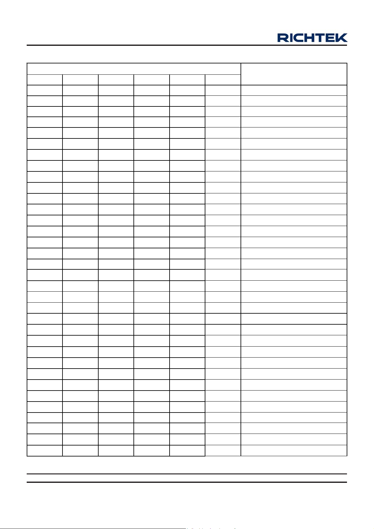
Table 4. Output Voltage Program (K8_M2)
Pin Name
VID5 VID4 VID3 VID2 VID1 VID0
0 0 0 0 0 0 1.5500
0 0 0 0 0 1 1.5250
0 0 0 0 1 0 1.5000
0 0 0 0 1 1 1.4750
0 0 0 1 0 0 1.4500
0 0 0 1 0 1 1.4250
0 0 0 1 1 0 1.4000
0 0 0 1 1 1 1.3750
0 0 1 0 0 0 1.3500
0 0 1 0 0 1 1.3250
0 0 1 0 1 0 1.3000
0 0 1 0 1 1 1.2750
0 0 1 1 0 0 1.2500
0 0 1 1 0 1 1.2250
0 0 1 1 1 0 1.2000
Nominal Output Voltage DACOUT
0 0 1 1 1 1 1.1750
0 1 0 0 0 0 1.1500
0 1 0 0 0 1 1.1250
0 1 0 0 1 0 1.1000
0 1 0 0 1 1 1.0750
0 1 0 1 0 0 1.0500
0 1 0 1 0 1 1.0250
0 1 0 1 1 0 1.0000
0 1 0 1 1 1 0.9750
0 1 1 0 0 0 0.9500
0 1 1 0 0 1 0.9250
0 1 1 0 1 0 0.9000
0 1 1 0 1 1 0.8750
0 1 1 1 0 0 0.8500
0 1 1 1 0 1 0.8250
0 1 1 1 1 0 0.8000
0 1 1 1 1 1 0.7750
1 0 0 0 0 0 0.7625
1 0 0 0 0 1 0.7500
All brandname or trademark belong to their owner respectively
DS8803A-05 August 2007www.richtek.com
14
To be continued
Page 15
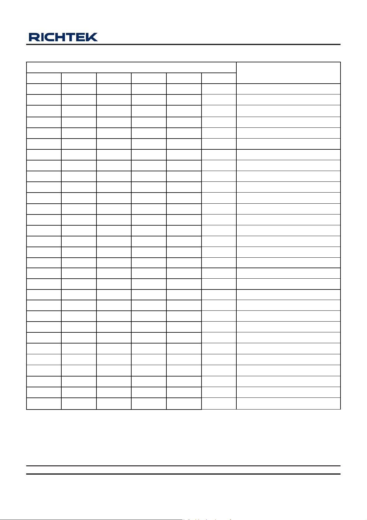
Table 4. Output Voltage Program (K8_M2)
RT8803A
Pin Name
VID5 VID4 VID3 VID2 VID1 VID0
1 0 0 0 1 0 0.7375
1 0 0 0 1 1 0.7250
1 0 0 1 0 0 0.7125
1 0 0 1 0 1 0.7000
1 0 0 1 1 0 0.6875
1 0 0 1 1 1 0.6750
1 0 1 0 0 0 0.6625
1 0 1 0 0 1 0.6500
1 0 1 0 1 0 0.6375
1 0 1 0 1 1 0.6250
1 0 1 1 0 0 0.6125
1 0 1 1 0 1 0.6000
1 0 1 1 1 0 0.5875
1 0 1 1 1 1 0.5750
1 1 0 0 0 0 0.5625
Nominal Output Voltage DACOUT
1 1 0 0 0 1 0.5500
1 1 0 0 1 0 0.5375
1 1 0 0 1 1 0.5250
1 1 0 1 0 0 0.5125
1 1 0 1 0 1 0.5000
1 1 0 1 1 0 0.4875
1 1 0 1 1 1 0.4750
1 1 1 0 0 0 0.4625
1 1 1 0 0 1 0.4500
1 1 1 0 1 0 0.4375
1 1 1 0 1 1 0.4250
1 1 1 1 0 0 0.4125
1 1 1 1 0 1 0.4000
1 1 1 1 1 0 0.3875
1 1 1 1 1 1 0.3750
Note: (1) 0 : Connected to GND
(2) 1 : Open
(3) The voltage above are load independent for desktop and server platforms. For mobile platforms the voltage above
correspond to zero load current.
All brandname or trademark belong to their owner respectively
DS8803A-05 August 2007 www.richtek.com
15
Page 16
RT8803A
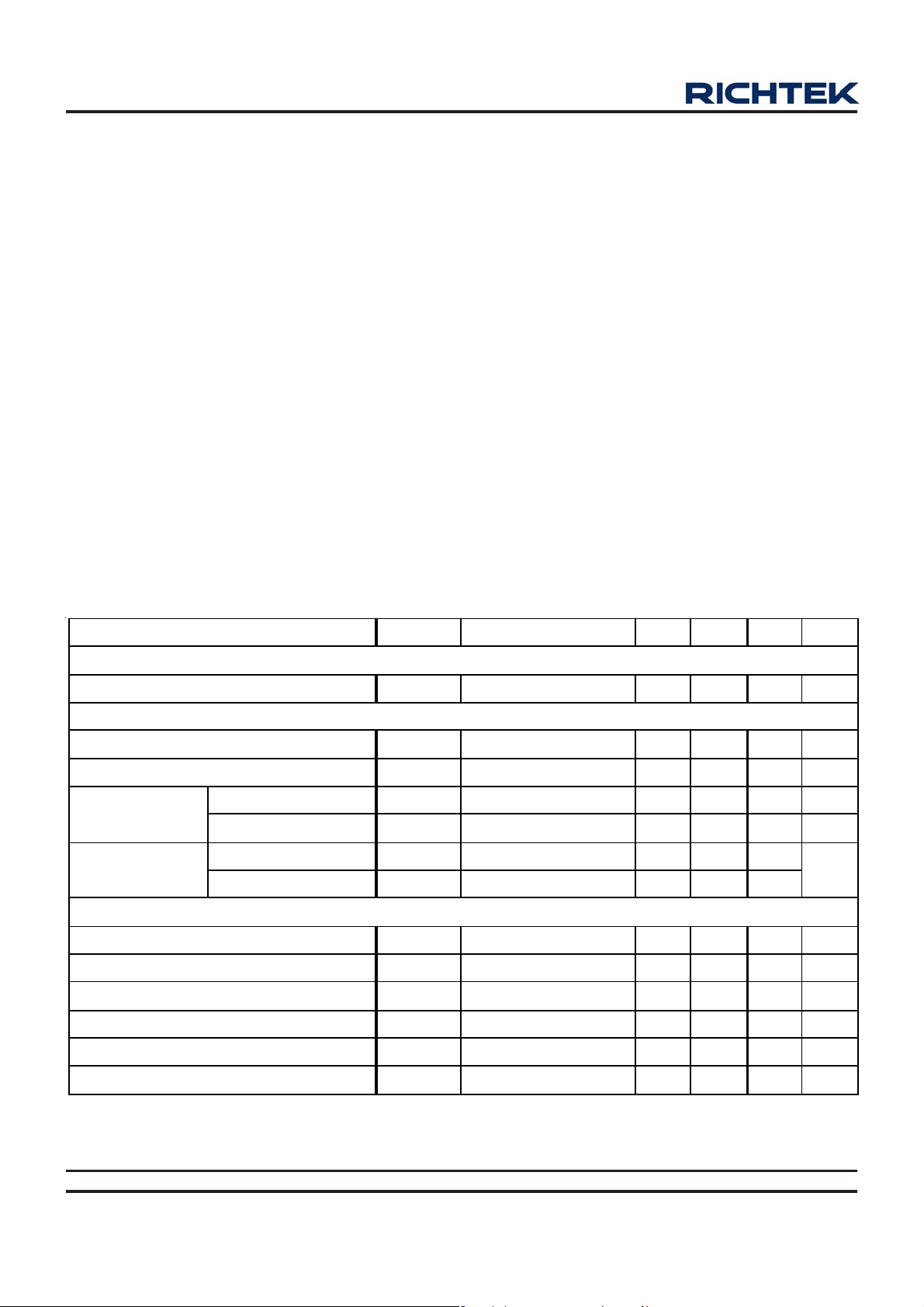
Absolute Maximum Ratings (Note 1)
z Supply V oltage, V
z Input, Output or I/O Voltage ---------------------------------------------------------------------------------- GND-0.3V to V
z Power Dissipation, P
------------------------------------------------------------------------------------------- 7V
DD
@ T
D
= 25°C
A
VQFN−32L 5x5-------------------------------------------------------------------------------------------------- 2.778W
z Package Thermal Re sistance (Note 4)
VQF N-32L 5x5, θJA--------------------------------------------------------------------------------------------- 36°C/W
z Junction T emperature------------------------------------------------------------------------------------------ 150°C
z Lead T e mperature (Soldering, 10 sec.)-------------------------------------------------------------------- 260°C
z Storage T emperature Range --------------------------------------------------------------------------------- −65°C to 150°C
z ESD Susceptibility (Note 2)
HBM (Human Body Mode) ----------------------------------------------------------------------------------- 2kV
MM (Ma chine Mode)------------------------------------------------------------------------------------------- 200V
Recommended Operating Conditions (Note 3)
z Supply V oltage, V
z Junction T emperature Range--------------------------------------------------------------------------------- −40°C to 125°C
z Ambient T emperature Range--------------------------------------------------------------------------------- −40°C to 85°C
------------------------------------------------------------------------------------------- 5V ± 10%
DD
Electrical Characteristics
(V
= 5V, TA = 25° C, unless otherwise specified)
DD
Parameter Symbol Test Conditions Min Typ Max Units
DD
+0.3V
V
Supply Current
DD
Nominal Supply Current IDD PWM 1,2,3 Open -- 12 16 mA
Power-On Reset
POR Threshold V
Hysteresis V
Trip (Low to High) V
V
Threshold
DVD
Hysteresis V
Trip (Low to High) V
VTT Threshold
Hysteresis V
VDD Rising 4.0 4.2 4.5 V
DDRTH
0.2 0.5 -- V
DDHYS
Enable 0.9 1.0 1.1 V
DVDTH
DVDHYS
TTTH
TTHYS
-- 60 -- mV
Enable 0.75 0.85 0.95
-- 0.1 --
V
Oscillator
Free Running Frequency f
Frequency Adjustable Range f
Ramp Amplitude ΔV
R
OSC
OSC_ADJ
50 -- 400 kHz
RRT = 2 0 k Ω -- 1.9 -- V
OSC
= 2 0 k Ω 180 200 220 kHz
RT
Ramp Valley VRV 0.7 1.0 -- V
Maximum On-Time of Each Channel Three Phase Operation 62 67 72 %
RT Pin Voltage VRT R
= 2 0 k Ω 0.9 1.0 1.1 V
RT
To be continued
16
All brandname or trademark belong to their owner respectively
DS8803A-05 August 2007www.richtek.com
Page 17
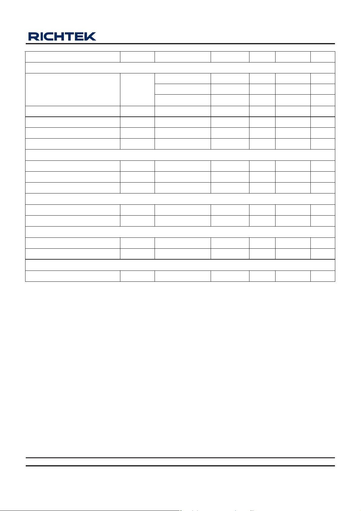
Parameter Symbol Test Conditions Min Typ Max Units
Reference and DAC
DACOUT Voltage Accuracy ΔV
DAC (VID0-VID125) Input Low
DAC (VID0-VID125) Input High
VID Pull-up Resistance
V
V
12 15 18
DAC
ILDAC
IHDAC
RT8803A
V
≥ 1V −0.5 -- +0.5 %
DAC
1V ≥ V
V
DAC
-- --
≥ 0.8V −5 -- +5 mV
DAC
< 0.8V −8 -- +8 mV
V
1/2V
TT
+ 0.2
1/2V
TT
− 0.2
-- -- V
kΩ
OFS Pin Voltage
R
V
OFS
= 100kΩ
OFS
0.9 1.0 1.1 V
Error Amplifier
DC Gain -- 65 -- dB
Gain-Bandwidth Product GBW -- 10 -- MHz
Slew Rate SR COMP = 10pF -- 8 --
V/μs
Current Sense GM Amplifier
CSN Full Scale Source Current
I
ISPFSS
CSN Current for OCP 150 -- --
100 -- --
μA
μA
Protection
Over-Voltage Trip (FB-DACOUT)
IMAX Voltage
ΔOVT
R
V
IMAX
IMAX
100 150 200 mV
= 20k
0.9 1.0 1.1 V
Power Good
Output Low Voltage
Note 1. Stresses listed as the above "Absolute Maximum Ratings" may cause permanent damage to the device. These are for
stress ratings. Functional operation of the device at these or any other conditions beyond those indicated in the
operational sections of the specifications is not implied. Exposure to absolute maximum rating conditions for extended
periods may remain possibility to affect device reliability.
Note 2. Devices are ESD sensitive. Handling precaution recommended.
Note 3. The device is not guaranteed to function outside its operating conditions.
Note 4. θ
is measured in the natural convection at TA = 25°C on a low effective thermal conductivity test board of
JA
JEDEC 51-3 thermal measurement standard.
V
PGOODL
I
PGOOD
= 4mA
-- -- 0.2 V
All brandname or trademark belong to their owner respectively
DS8803A-05 August 2007 www.richtek.com
17
Page 18
RT8803A
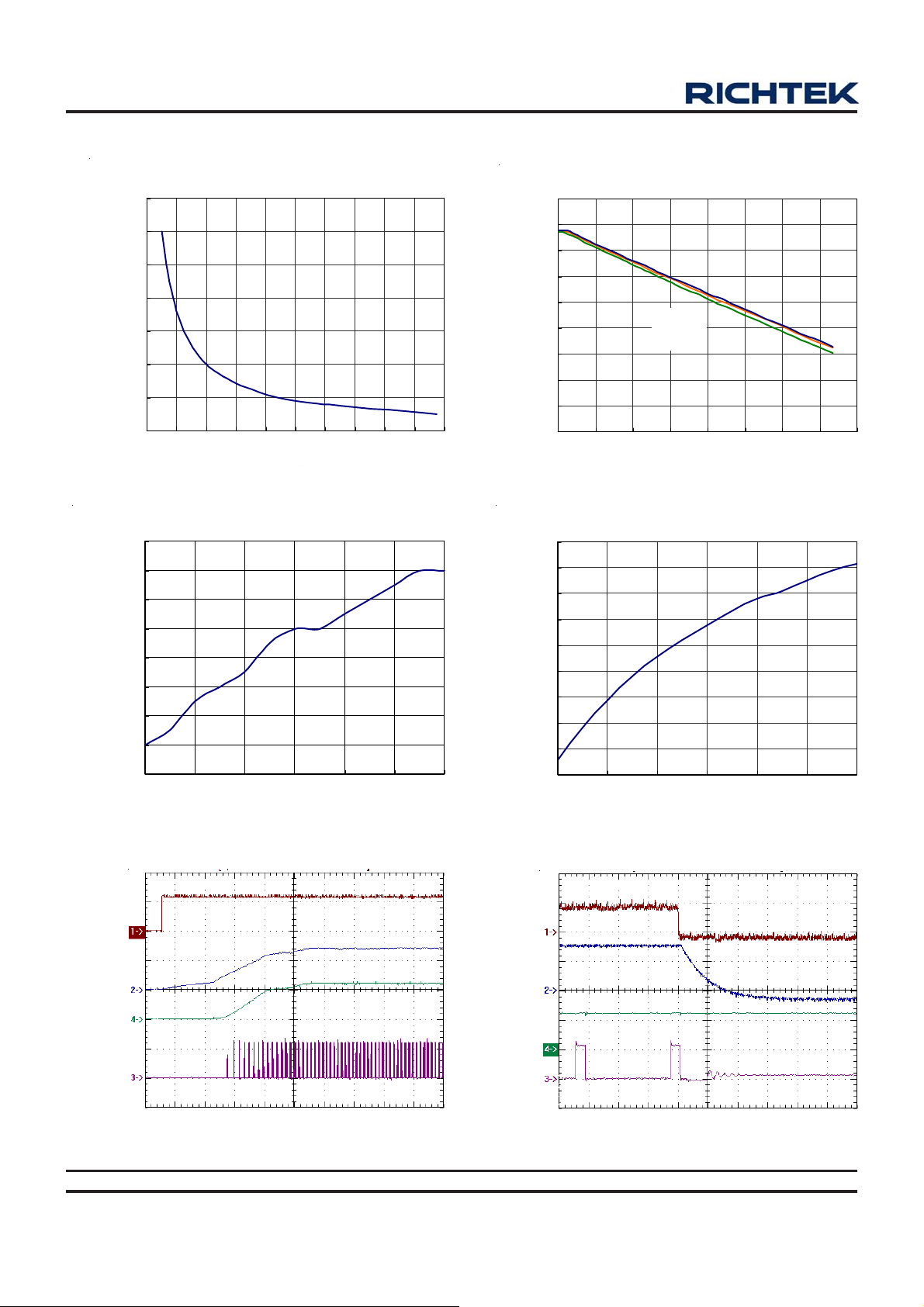
Typical Operating Characteristics
Frequency vs. R
700
600
500
400
300
200
Frequency ( kHz)
100
0
0 102030405060708090100
(kΩ)
RRT (kٛ)
RT
Output Voltage vs. Temperature
1.264
1.262
1.26
1.258
1.256
1.254
1.252
Output Voltage (V)
1.25
1.248
-20 0 20 40 60 80 100
Temperature
(°C)
450
400
350
300
250
200
150
Positive Duty (ns)
100
50
0
0 25 50 75 100 125 150 175 200
PHASE 3
PHASE 1
PHASE 2
ISN (uA)
Frequency vs. Temperature
322
320
318
316
314
312
310
Frequency ( kH z)
308
306
304
-20 0 20 40 60 80 100
GM
Temperature
(°C)
DVD
(1V/Div)
SS
(1V/Div)
V
OUT
(1V/Div)
PHASE 3
(10V/Div)
18
Power On from DVD
Time (1ms/Div)
All brandname or trademark belong to their owner respectively
DVD
(1V/Div)
SS
(1V/Div)
V
OUT
(1V/Div)
PHASE 3
(10V/Div)
Power Off from DVD
Time (1μs/Div)
DS8803A-05 August 2007www.richtek.com
Page 19
RT8803A
VCC12
(10V/Div)
SS
(1V/Div)
V
OUT
(1V/Div)
PHASE 3
(10V/Div)
VCC5
(5V/Div)
SS
(1V/Div)
V
OUT
(1V/Div)
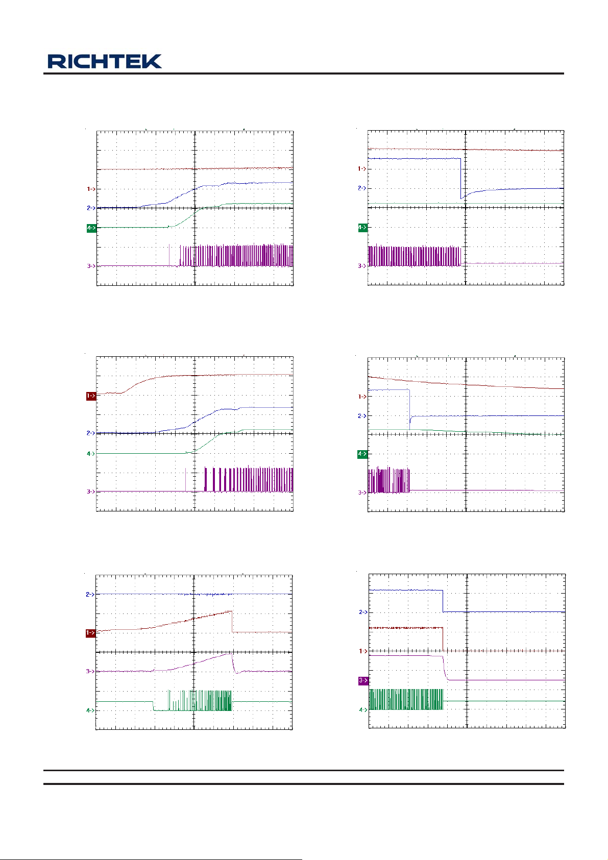
Power On from VCC12
Time (1ms/Div)
Power On from VCC5
VCC12
(10V/Div)
SS
(1V/Div)
V
OUT
(1V/Div)
PHASE 3
(10V/Div)
VCC5
(5V/Div)
SS
(1V/Div)
V
OUT
(1V/Div)
Power Off from VCC12
Time (1ms/Div)
Power Off from VCC5
PHASE 3
(10V/Div)
Time (1ms/Div)
Power On with OCP
VR_Ready
(1V/Div)
SS
(2V/Div)
V
OUT
1V/Div)
PWM
(5V/Div)
Time (500μs/Div)
All brandname or trademark belong to their owner respectively
DS8803A-05 August 2007 www.richtek.com
PHASE 3
(10V/Div)
VR_Ready
(1V/Div)
SS
(2V/Div)
V
OUT
(1V/Div)
PWM
(5V/Div)
Time (25ms/Div)
Output Short Circuit
Time (1ms/Div)
19
Page 20
RT8803A
V
OUT
(20mV/Div)
I
OUT
(40A/Div)
V
OUT
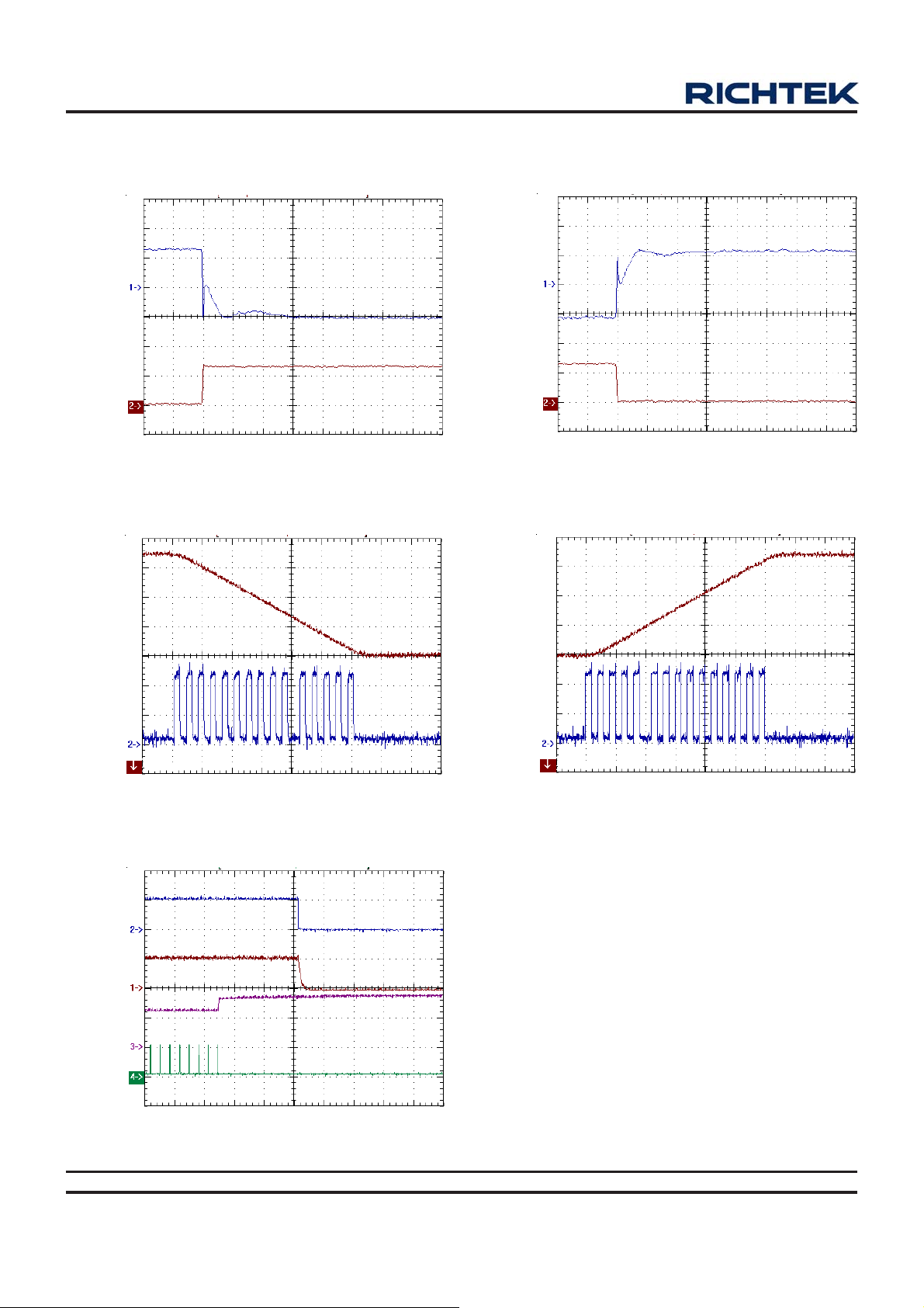
Droop
V
OUT
(20mV/Div)
I
OUT
(40A/Div)
V
Overshoot
OUT
V
OUT
(200mV/Div)
VID0
(500mV/Div)
Time (2μs/Div)
Dynamic VID
Time (50μs/Div)
OVP
V
OUT
(200mV/Div)
VID0
(500mV/Div)
Time (2μs/Div)
Dynamic VID
Time (50μs/Div)
VR_Ready
(1V/Div)
SS
(2V/Div)
FB
(1V/Div)
PWM
(5V/Div)
20
Time (10μs/Div)
All brandname or trademark belong to their owner respectively
DS8803A-05 August 2007www.richtek.com
Page 21
Applications Information
RT8803A is a multi-phase DC/DC controller specifically
designed to deliver high quality power for next generation
CPU. RT8803A controls a special power-on sequence &
monitors the thermal condition of VR module to meet the
VRD11 requirement. Phase currents are sensed by
innovative time-sharing DCR current sensing technique
for channel current bala nce, droop tuning, and over current
protection. Using one common GM amplifier for current
sensing eliminates offset errors and linearity variation
between GMs. As sub-milli-ohm-grade inductors are
widely used in modern mother boards, slight mismatch
of GM a mplifiers off set and linearity results in considerable
current shift between phases. The time-sharing DCR
current sensing technique is extremely important to
guarantee pha se current balance in ma ss production.
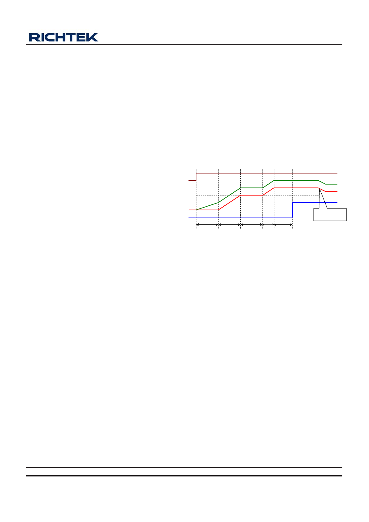
RT8803A
with Intel® VRD11 specification as shown in Figure 1. A
time-varia nt internal current source charges the ca pacitor
connected to SS pin. SS voltage ramps up piecewise
linearly and locks VID_DAC output with a specified voltage
drop. Consequently, V
VID_DAC output and meet Intel® VRD11 requirement.
VR_READY output is pulled high by external resistor when
V
reaches VID_DAC output with 1~2ms delay. An
CORE
SS capacitor about 47nF is recommend for VRD11
compliance.
VDD POR, DVD, and VTT/EN ready
1.1V
is built up according to
CORE
SS
V
CORE
VR_Ready
Converter Initialization, Phase Selection, and
Power Good Function
The RT8803A initiates only after 3 pins are ready: VDD
pin power on reset (POR), VTT/EN pin en abled, and D V D
pin is higher than 1V . V D D POR is to ma ke sure RT8803A
is powered by a voltage for normal work. The rising
threshold voltage of VDD POR is 4.2V typically. At VDD
POR, RT8803A che cks PWM3, PWM4 and PWM5 status
to determine phase number of operation. Pull high PWM3
for two-pha se operation; pull high PWM4 for three-pha se
operation; pull high PWM5 for four-pha se operation. The
unused current sense pins should be connected to GND
or left floating.
VTT/EN a cts as a chi p enable pin a nd receives signal from
FSB or other power management IC.
DVD is to make sure that ATX12V is ready for drivers to
work normally . Connect a voltage divider from A TX12V to
D V D pin as shown in the Typical Application Circuit. Ma ke
sure that DVD pin voltage is below its threshold voltage
before drivers are ready a nd above its thre shold voltage
for minimum A TX12V during normal operation.
VID on the fly
1~2ms 1~2ms 1~2ms 1~2ms
1~2ms
Figure 1. Ti mming Diagra m During Soft Start Interval
Voltage Control
CPU V
voltage is Kelvin sensed by FB and FBRTN
CORE
pins and precisely regulated to VID_DAC output by internal
high gain Error Amplifier (EA). The sensed signal is also
used for power good and over voltage function. The typical
OVP trip point is 170mV above VID_DAC output. RT8803A
pulls PWM outputs low and latches up upon OVP tri p to
prevent damaging the CPU. It ca n only restart by resetting
one of VDD, D V D, or VTT/EN pin.
RT8803A supports Intel VRD10.x, VRD11, AMD K8 and
AMD K8_M2 VID specification.
The change of VID_DAC output at VID on the fly is also
smoothed by capacitor connected to SS pin.
Consequently, Vcore shifts to its new position smoothly
a s shown in Figure 2.
If any one of V DD, VTT/EN, a nd D V D is not ready , RT8803A
keeps its PWM outputs high impedance and the
companion drivers turn off both upper and lower
MOSFETs. After VDD, VTT/EN, and DVD are ready,
RT8803A initiates its soft start cycle that is compliant
All brandname or trademark belong to their owner respectively
DS8803A-05 August 2007 www.richtek.com
21
Page 22
RT8803A
PWM3
V
CORE
VID7
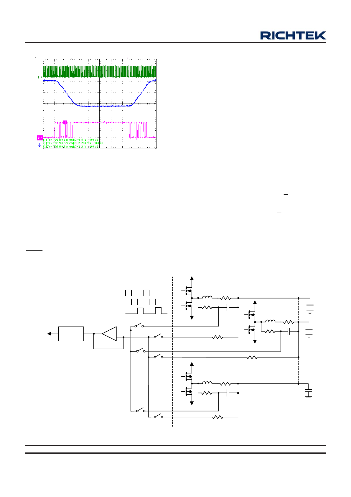
Figure 2. Vcore Response at VID on the Fly
DCR Current Sensing
RT8803A adopts an innovative time-sharing DCR current
sensing technique to sense the pha se currents for pha se
current balance (phase thermal balance) and load line
regulation as shown in Figure 3. Current sen sing amplifier
GM samples and holds voltages VCx across the current
sensing capacitor Cx by turns in a switching cycle.
According to the Basic Circuit Theory, if
Lx
DCRx
LX
DCRxI VCxthenCx Rx
×=×=
Consequently, the sensing current IX is proportional to
inductor current ILX and is expressed a s :
DCRxI
×
LX
I
=
X
R
CSNX
The sensed current IX is used for current balance a nd droop
tuning as described as followed. Since all phases share
one common GM, GM off set and linearity vari ation effect
is eliminated in practical applications. As sub-milli-ohmgrade inductors are widely used in modern mother boards,
slight mismatch of GM a mplifiers offset a nd linearity results
in considerable current shift between phases. The timesharing DCR current sensing technical is extremely
important to guarantee phase current balance in mass
production.
Phase Current Balance
The sampled a nd held pha se current IX are summed and
averaged to get the averaged current . Each phase
XI
current IX then is compared with the averaged current.
The difference between IX and is injected to
XI
corresponding PWM comparator. If phase current IX is
smaller than the averaged current , RT8803A increases
the duty cycle of corresponding phase to increase the
phase current a ccordingly a nd vice versa.
22
IX = I
x DCRX/R
LX
I
X
CSA: Current Sense Amplifier
CSNX
S/H CKT
CSA
T1
T2
T3
ISP1
+
-
T1
T3
T2
T1
T3
T2
ISN1
ISP3
ISN23
ISP2
ISN23
L1
R1
L2
R2
R
R
CSN1
CSN2
DCR1
C1
+ VC1 -
DCR2
C2
+ VC2 -
R
Figure 3
All brandname or trademark belong to their owner respectively
CSN3
L3
DCR3
R3
C3
+ VC3 -
DS8803A-05 August 2007www.richtek.com
Page 23
I
OFS
4
R
DAC
FB1
-
EA
+
V
ADJ
-
+
COMP
X4I
R
ADJ
V
CORE
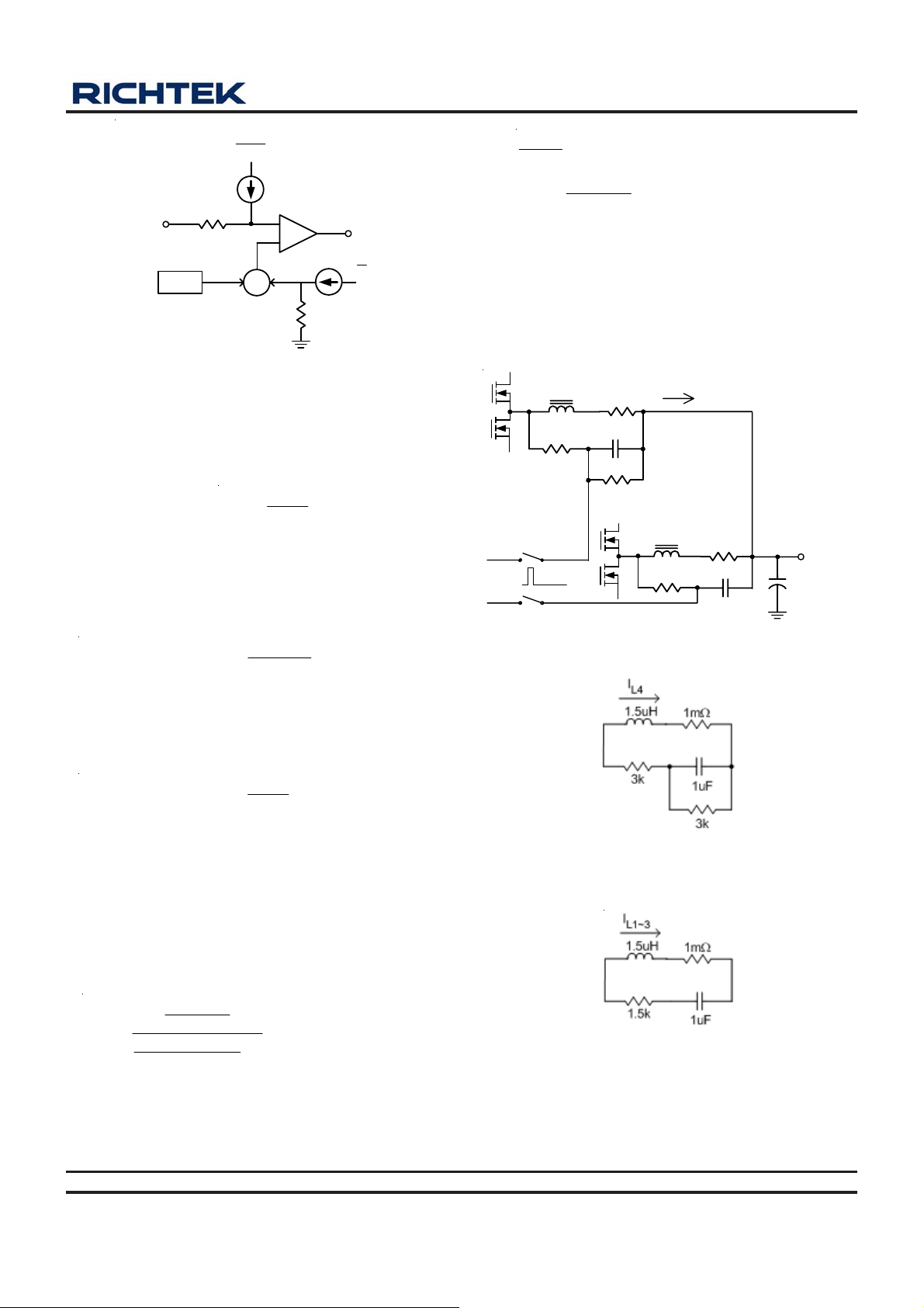
Figure 4. Load Line and Off set Function
Output V oltage Offset Function
To meet Intel® requirement of initial offset of load line,
RT8803A provides programmable initial offset function.
External resistor R
generate offset current
, where V
through R
is 1V typical. One quarter of I
OFS
as shown in Figure 4. Error amplifier would
FB1
hold the inverting pin equal to V
voltage is subtracted from V
and voltage source at OFS pin
OFS
V
OFS
I =
OFS
R
OFS
OFS
- V
. Thus output
ADJ
for a constant of fset
DAC
- V
DAC
ADJ
flows
voltage.
R
V V V
ADJDACCORE
FB1
− −=
R4
×
OFS
A positive output voltage offset is possible by connecting
R
to VDD instead of to GND. Please note that when
OFS
R
is connected to V DD, V
OFS
half of I
flows through R
OFS
V V V + −=
ADJDACCORE
is VDD − 2V typically and
OFS
FB1
R
R
. V
FB1
OFS
is rewritten as :
CORE
RT8803A
L
If
With other phase kept uncha nged, this pha se would share
(RPX+Rx)/R
and 7 show different current ratio setting for the power
stage when Phase 3 is progra mmed 2 ti mes current tha n
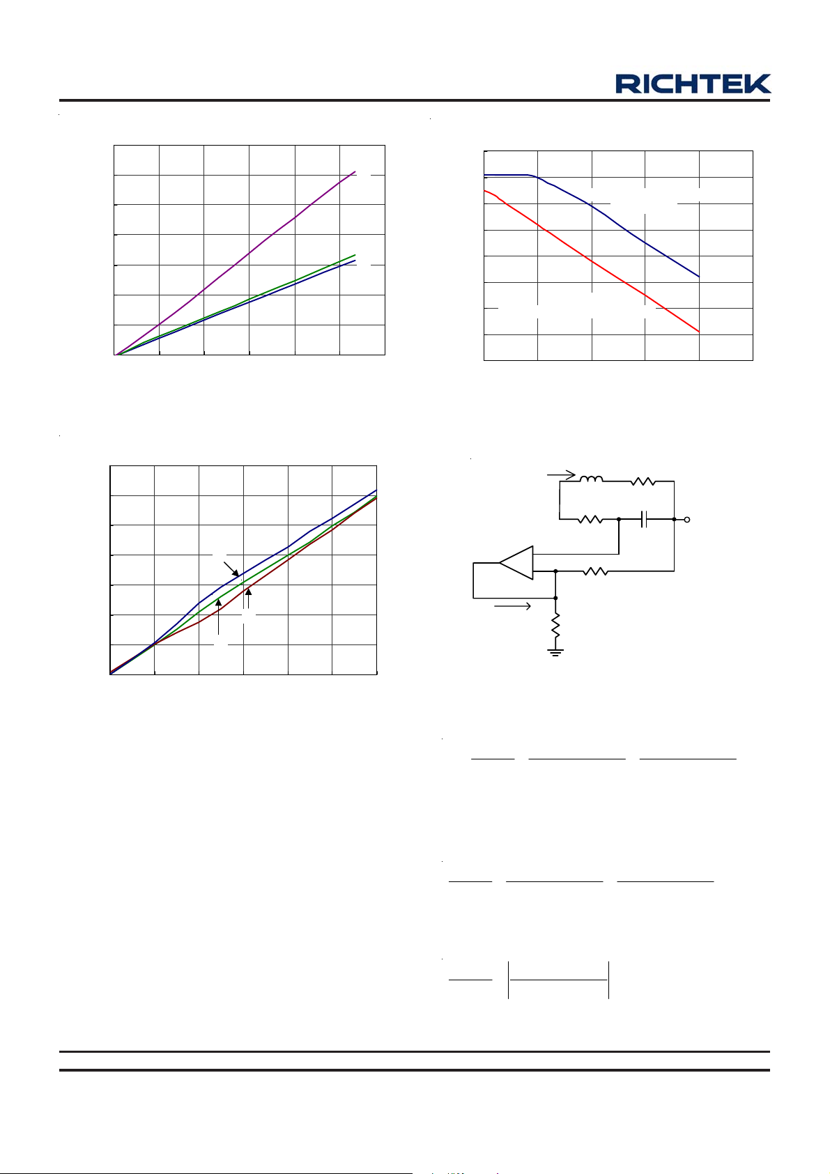
other phase s. Figure 8 and 9 compare the above current
ratio setting results.
X
DCRx
VCx
T
thenCx )//R(R
×=
PXX
R
PX
=
RRx
+
PX
times current than other phases. Figure 6
PX
L
X
DCRx
Rx
VCx
+-
Cx
R
PX
LX
DCRxI
××
I
LX
+
Figure 5
V
OUT
Current Ratio Setting
Current ratio adjustment is possible a s described below .
Figure 6. GM3 Setting for current ratio function
It is important for achieving thermal balance in practical
application where thermal condition s between phases are
not identical. Figure 5 shows the application circuit of GM
for current ratio requirement. According to Basic Circuit
Theory
R
PX
RRx
+
VCx
=
PX
CxRSRx
××
PX
RRx
+
PX
1
+
DS8803A-05 August 2007 www.richtek.com
DCRxI
××
LX
Figure 7. GM1~2 Setting f or current ratio function
All brandname or trademark belong to their owner respectively
23
Page 24
RT8803A
35
30
25
20
(A)
L
I
15
10
5
0
0 153045607590
I
(A)
OUT
Figure 8
Current Balance Function
35
30
25
Current Ratio Function
20
(A)
L
I
15
I
L3
Load Line without dead zone at light loads
1.31
I
L3
I
L2
I
L1
1.3
1.29
1.28
w/o Dead Zone Compensation
R
open
CSN
(V)
1.27
CORE
V
1.26
R
= 82k
1.25
1.24
1.23
w/i Dead Zone Compensation
0 5 10 15 20 25
CSN2
I
OUT
(A)
Figure 10
GMx
I
LX
+
-
Lx
Rx
R
CSN
DCRx
Cx
+-
VCx
V
OUT
10
5
0
0 20406080100120
I
L2
I
L1
I
(A)
OUT
Figure 9
Dead Zone Elimination
RT8803A samples and holds inductor current at 50%
period by time-sharing sourcing a current IX to R
CSN
. At
light load condition when inductor current is not balance,
voltage VCx across the sensing capacitor would be
negative. It needs a negative IX to sense the voltage.
However, RT8803A CANNOT provide a negative IX and
consequently cannot sense negative inductor current. This
results in dead zone of load line performa nce a s shown in
Figure 10. Therefore a technique a s shown in Figure 1 1 is
required to eliminate the dead zone of load line at light
load condition.
Ix
R
CSN2
Figure 1 1. Application circuit of GM
Referring to Figure 1 1, IX is expressed as :
X
where I
V
I
R
CSN2
LX_50%
OUT
LX_66%
+=
R
×
CSN2
LX_66%
+
DCRxI
is the of inductor current at 50% period. To
R
×
CSN
DCRxI
(1)
make sure RT8803A could sense the inductor current,
right hand side of Equation (1) should always be positive:
R
×
CSN
DCRxI
0
≥
(2)
V
OUT
R
CSN2
Since R
DCRxI
R
×
CSN2
LX_66%
+
>> DCRx in p ractical application, Equation (2)
CSN
LX_66%
+
could be simplified as :
DCRxI
V
R
OUT
CSN2
≥
LX_66%
R
×
CSN
24
All brandname or trademark belong to their owner respectively
DS8803A-05 August 2007www.richtek.com
Page 25
RT8803A
LX
CSNX
IMAX
IMAX
X
CSNX
XLX(MAX)
IMAX
IMAX
IMAXX(MAX)
IMAXX(MAX)
R
R
R
V
2
3
DCR
R
II
R
V
2
3
I
2
3
I
I
2
1
I
3
1
××=×=
×==
=
For example, assuming the negative inductor current is
I
= −5A at no load, then for
LX_50%
R
330Ω, R
CSN
1.3V
R
CSN2
R
≤ 85.8kΩ
CSN2
Choose R
CSN2
≥
= 160Ω, V
ADJ
330
= 82kΩ
= 1.300V
OUT
Ω×−
1m5A
Ω
Figure 10 shows that dead zone of load line at light load
is eliminated by applying this technique.
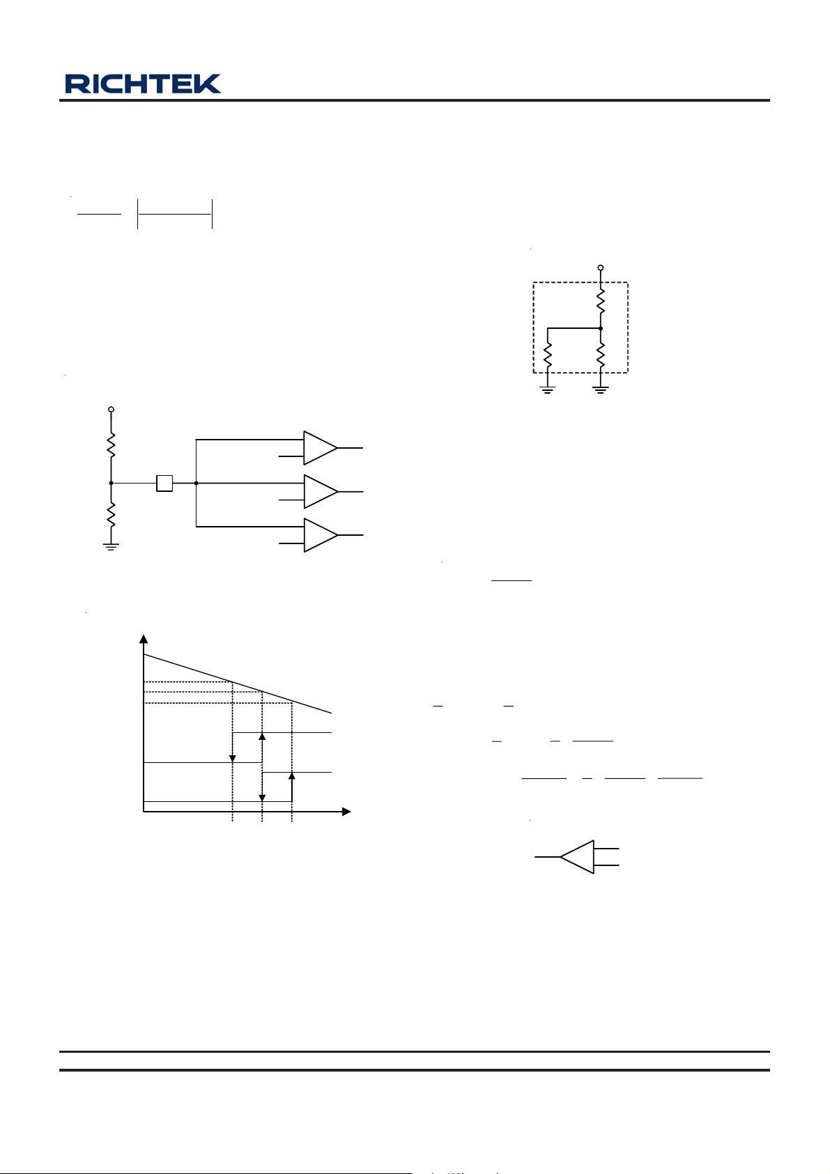
VR_HOT & VR_F AN Setting
V
CC
5V
CC
CC
CC
+
CMP
-
+
CMP
-
+
CMP
-
Q1
Q2
Q3
V
TSEN
R1
R
NTC
TSEN
0.39 x V
0.33 x V
0.28 x V
Figure 12
V
0.39 x V
0.33 x V
0.28 x V
TSEN
CC
CC
CC
V
is inversely proportional
TSEN
to Temperature.
If R
is connected as in Figure 14, R
ADJ
R
), which is a negative temperature correlated
NTC
= R1 + (R2//
ADJ
resistance. By properly selecting R1 a nd R2, the positive
temperature coefficient of DCR can be canceled by the
negative temperature coefficient of R
. Thus the load
ADJ
line will be thermally compensated.
ADJ
R1
R
ADJ
Figure 14. R
R
NTC
Connection for Thernal Compensation
ADJ
R2
Over Current Protection
Phase current OCP
RT8803A uses an external resistor R
IMAX pin to generate a reference current I
current protection :
V
I =
IMAX
where V
IMAX
R
IMAX
is typical 1.0V . OCP comparator compares
IMAX
each sensed phase current IX with this reference current
as shown in Figure 15. Equivalently , the maxi mum pha se
current I
is calculated as below:
LX(MAX)
connected to
IMAX
IMAX
for over
VR_FAN
VR_HOT
Figure 13. VR_HOT and VR_F AN Signal vs TSEN V oltage
Load Line Setting and Thermal Compensation
V
= Sum(IX) x R
ADJ
= LL x I
V
= V
OUT
DAC
OUT
− V
LL = DCR(PTC) x R
ADJ
ADJ
= V
ADJ
= (DCR x R
− LL x I
DAC
(NTC) / R
CSN
ADJ
OUT
/ R
Temperature
) x I
CSN
OUT
OCP Comparator
1/3 I
+
-
1/2 I
X
IMAX
Figure 15. Over Current Comparator
DCR is the inductor DCR which is a PTC resista nce.
All brandname or trademark belong to their owner respectively
DS8803A-05 August 2007 www.richtek.com
25
Page 26
RT8803A
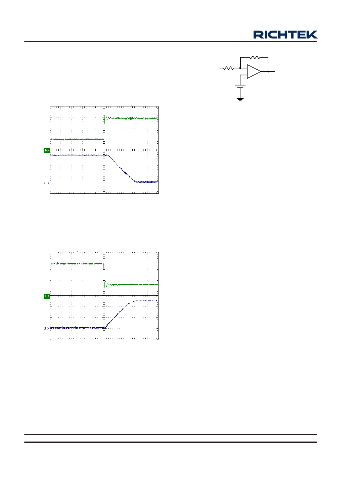
Error Amplifier Characteristic
For fast response of converter to meet stringent output
current transient response, R T8803A provides large slew
rate capa bility and high gain-bandwidth perf ormance.
EA Falling Slew Rate
V
FB
V
COMP
CH1:(500mV/Div)
CH2:(2V/Div)
Time (250ns/Div)
Figure 16. EA Rising T ra n sient with 10pF Loading ;
Slew Rate = 10V/μs
4.7k
4.7k
B
-
EA
+
V
REF
A
Figure 18. Gain-Ba ndwidth Mea surement by signal A
divided by signal B
Design Procedure Suggestion
a. Output filter pole and zero (Inductor, output capacitor
value & ESR).
b. Error amplifier compensation & saw-tooth wave
amplitude (compen sation network).
c. Kelvin sense for V
CORE
.
Current Loop Setting
a. GM amplifier S/H current (current sense component
DCR, ISPX and ISNX pin external resistor value).
b. Over-current protection trip point (R
IMAX
resistor).
EA Rising Slew Rate
V
FB
V
COMP
Time (250ns/Div)
CH1:(500mV/Div)
CH2:(2V/Div)
Figure 17. EA Falling T ra n sient with 10pF Loading ;
Slew Rate = 8V/μs
VRM Load Line Setting
a. Droop a mplitude (ADJ pin resistor).
b. No load offset (R
CSN
)
c. DAC offset voltage setting (OFS pin & compensation
network resistor).
d. T emperature coefficient compensation(TSEN external
resister & thermistor, resistor between ADJ a nd GND.)
Power Sequence & SS
D VD pin external resistor and SS pin capacitor.
PCB Layout
a.Kelvin sense for current sense GM a mplifier in put.
b.Refer to layout guide for other items.
26
All brandname or trademark belong to their owner respectively
DS8803A-05 August 2007www.richtek.com
Page 27
Outline Dimension
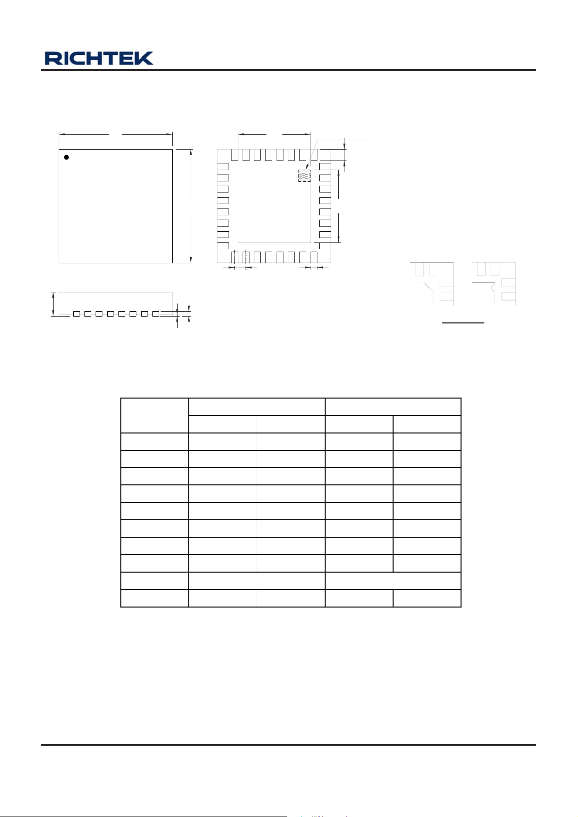
RT8803A
D
E
e
A
A3
A1
D2
SEE DETAIL A
1
b
L
E2
1
2
1
2
DETAIL A
Pin #1 ID a nd T ie Bar Mark Option s
Note : The configuration of the Pin #1 identifier is optional,
but must be located within the zone indicated.
Dimensions In Millimeters Dimensions In Inches
Symbol
Min Max Min Max
A 0.800 1.000 0.031 0.039
A1 0.000 0.050 0.000 0.002
A3 0.175 0.250 0.007 0.010
b 0.180 0.300 0.007 0.012
D 4.950 5.050 0.195 0.199
D2 3.400 3.750 0.134 0.148
E 4.950 5.050 0.195 0.199
E2 3.400 3.750 0.134 0.148
e 0.500 0.020
L 0.350 0.450
Richtek Technology Corporation
Headquarter
5F, No. 20, Taiyuen Street, Chupei City
Hsinchu, Taiwan, R.O.C.
Tel: (8863)5526789 Fax: (8863)5526611
0.014 0.018
V-Type 32L QFN 5x5 Package
Richtek Technology Corporation
Taipei Office (Marketing)
8F, No. 137, Lane 235, Paochiao Road, Hsintien City
Taipei County, Taiwan, R.O.C.
Tel: (8862)89191466 Fax: (8862)89191465
Email: [email protected]
DS8803A-05 August 2007 www.richtek.com
27
 Loading...