

Page 1
Single Synchronous Buck Controller
RT8202/A/B
General Description
The RT8202/A/B PWM controller provides high efficiency ,
excellent transient response, a nd high DC output a ccuracy
needed for stepping down high voltage batteries to
generate low voltage CPU core, I/O, and chipset RAM
supplies in notebook computers.
The constant on-time PWM control sche me handles wide
input/output voltage ratios with ea se and provides 100ns
“instant-on” response to load tran sients while maintaining
a relatively constant switching frequency .
The RT8202/A/B achieves high efficiency at a reduced
cost by eliminating the current sense resistor found in
traditional current mode PWMs. Efficiency is further
enhanced by its ability to drive very large synchronous
rectifier MOSFET s. The buck conversion allows this device
to directly step down high voltage batteries for the highest
possible efficiency . The RT8202/A/B is intended f or CPU
core, chipset, DRAM, or other low voltage supplies as
low as 0.75V. RT8202 is available in WQFN-16L 4x4,
RT8202A is available in WQF N-16L 3x3 and R T8202B is
available in WQF N-14L 3.5x3.5 pack ages.
Ordering Information
RT8202/A/B
Package Type
QW : WQFN-16L 4x4 (W-Type) (RT8202)
QW : WQFN-16L 3x3 (W-Type) (RT8202A)
QW : WQFN-14L 3.5x3.5 (W-Type) (RT8202B)
Lead Plating System
P : Pb Free
G : Green (Halogen Free and Pb Free)
Note :
Richtek products are :
` RoHS compliant and compatible with the current require-
ments of IPC/JEDEC J-STD-020.
` Suitable for use in SnPb or Pb-free soldering processes.
Marking Information
For marking information, contact our sales re presentative
directly or through a Richtek distributor located in your
area.
Features
zz
Ultra-High Efficiency
z
zz
zz
z Resistor Programmable Current Limit by Low Side
zz
R
Sense (Lossless Limit) or Sense Resistor
DS(ON)
(High Accuracy)
zz
z Quick Load Step Response within 100ns
zz
zz
z 1% V
zz
zz
z Adjustable 0.75V to 3.3V Output Range
zz
zz
z 4.5V to 26V Battery Input Range
zz
zz
z Resistor Programmable Frequency
zz
zz
z Over/Under Voltage Protection
zz
zz
z 2 Steps Current Limit During Soft-Start
zz
zz
z Drives Large Synchronous-Rectifier FET s
zz
zz
z Power Good Indicator
zz
zz
z RoHS Compliant and 100% Lead (Pb)-Free
zz
Accuracy over Line and Load
OUT
Applications
z Notebook Computers
z CPU Core Supply
z Chipset/RAM Supply a s Low as 0.75V
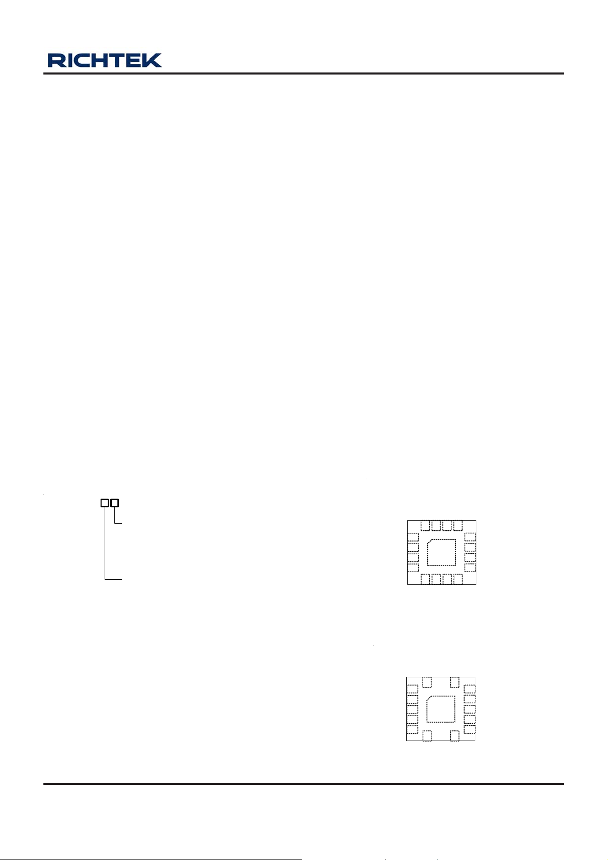
Pin Configurations
(TOP VIEW)
TON
EN/DEM
BOOT
NC
13141516
UGATE
GND
17
8765
PGND
141
15
87
12
11
10
9
LGATE
BOOT
13
12
11
10
96
PGND
PHASE
OC
VDDP
UGATE
PHASE
OC
VDDP
VOUT
1
2
VDD
FB
PGOOD
GND
3
4
NC
WQFN-16L 4x4/WQFN-16L 3x3
EN/DEM
2
TON
3
VOUT
VDD
FB
PGOOD LGATE
GND
4
5
GND
WQFN-14L 3.5x3.5
DS8202/A/B-05 April 2011 www.richtek.com
1
Page 2
RT8202/A/B
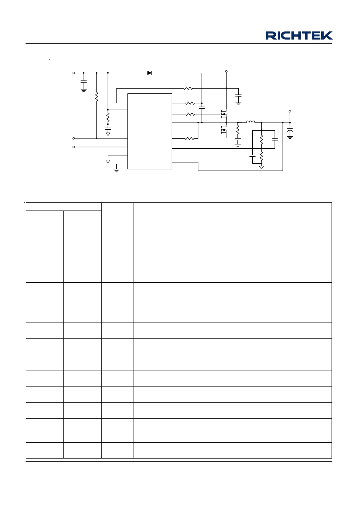
Typical Application Circuit
D
1
A
B
2
T
5
V
P
D
D
V
5
O
O
D
P
G
C
D
/
C
M
M
E
1
C
µ
F
1
R
2
k
1
5
1
R
0
1
C
µ
1
O
N
T
V
D
D
V
D
2
F
D
P
G
O
E
D
/
N
N
D
G
G
P
N
Functional Pin Description
Pi n No.
RT8202/A RT8202B
1 3 VOU T
2 4 VDD
3 5 FB
4 6 PGO OD
5, 14 -- NC No In ternal Connection.
6,
Exposed Pad
(17)
7,
Exposed Pad
(15)
7 8 PGN D Power Groun d.
8 9 LGATE
9 10 VDD P
10 11 OC
11 12 PHASE
12 13 UGATE
13 14 BOOT
15 1 EN/DEM
16 2 TON
Pin Name Pin Function
VOUT Sense Input. Conn ect to the output of PWM converter. VOUT is an
input of the PWM con trol ler .
Analog Supply Voltage Input for the internal analog integrated circuit.
B y pa s s to GN D with a 1 μF ceramic capacito r.
VOUT Feedback Input. Connect FB to a resistor voltage divider from
VOUT to GND to adjust the output from 0.75V to 3.3 V.
Power Good Signal Open-Drain Output of PWM Converter. This pin will
be pulled high when the output voltage is within the target range.
GND
Ground for Analog Circuitry. The expos ed pad must be sol der ed t o a large
PCB and connected to GND for maximum power dissipation.
Low side N-MOSFET Gate-Drive Output for PWM. This pin swings
betw een G ND and VDDP .
VDDP is th e gate driver supply for the external MO SFETs. Bypass to
GND with a 1μF ceramic capacitor .
PWM Current Limit Set ting and sense. Con nect a resistor betwe en OC to
PHASE for c urre n t li mit sett ing .
Inductor Connection. This pin is not only the zero-current-sense input for
the PWM converter, but also the UGATE high side gate driver return.
High Side N-MOSFET Floating Gate-Driver Output for the PWM
con ver te r. This pi n swi ngs betw een PHASE and BOOT.
Boost Capacitor Connection for PWM Converter. Connect an external
ceramic capacitor to PHAS E and an ext er nal diode to VDDP.
PWM Enable and Operation Mode Selection Input. Connect to VDD for
diode-emulation mode, connect to GND for shutdown mode and floating
the pi n for CCM mode.
VIN Sense Input. Connect to VIN through a resistor. TON is an input of
the P WM controller.
4
T
R
8
/
2
A
0
2
B
/
T
O
O
B
P
D
U
G
A
T
E
A
P
H
S
E
A
G
L
T
E
O
D
E
M
O
C
F
B
V
T
U
O
V
I
N
4
.
5
V
o
t
2
6
V
R
3
1
M
4
4
R
2
2
.
R
5
1
R
6
3
C
0
.
1
F
0
0
µ
2
k
Q
A
O
7
0
2
4
C
1
0
µ
F
1
Q
4
O
A
7
0
2
L
1
2
H
4
µ
.
R
7
5
C
C
8
0
.
1
µ
F
R
1
2
R
2
0
V
U
O
T
2
V
1
.
7
C
2
2
0
µ
6
C
8
k
9
k
F
DS8202/A/B-05 April 2011www.richtek.com
2
Page 3
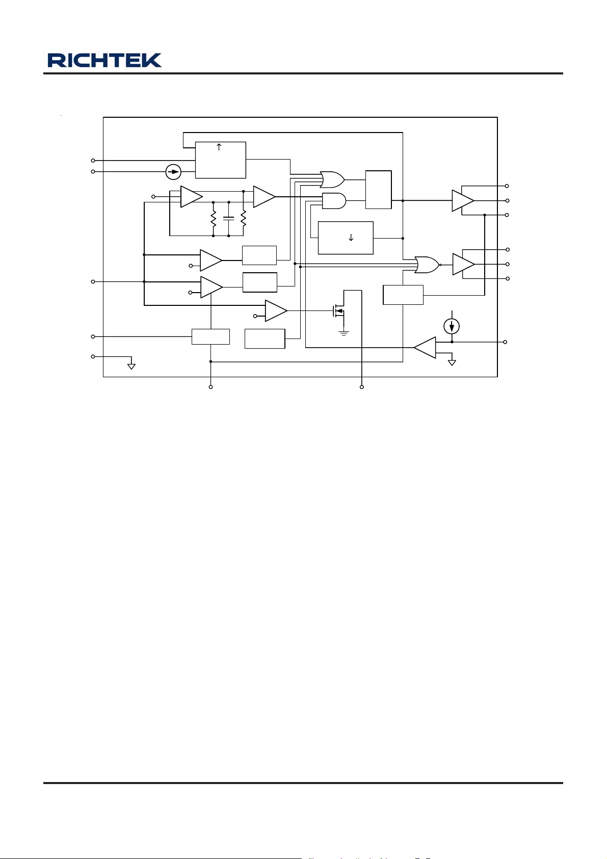
Function Block Diagram
TRIG
VOUT
TON
+
70% V
-
GM
+
0.75V V
REF
REF
-
REF
+
-
+
SS Timer
SS(Internal)
115% V
FB
VDD
GND
On-time
Compute
1-SHOT
OV
UV
90% V
+
Latch
S1 Q
Latch
S1 Q
REF
Thermal
Shutdown
Comp
+
R
QS
Min. T
OFF
QTRIG
1-SHOT
Emulation
Diode
RT8202/A/B
BOOT
DRV
DRV
20uA
+
-
UGATE
PHASE
VDDP
LGATE
PGND
OC
EN/DEM
PGOOD
DS8202/A/B-05 April 2011 www.richtek.com
3
Page 4

RT8202/A/B
Absolute Maximum Ratings (Note 1)
z Input V oltage, TON to GN D ---------------------------------------------------------------------------------------------- −0.3V to 32V
z BOOT to GND -------------------------------------------------------------------------------------------------------------- −0.3V to 38V
z PHASE to BOOT ---------------------------------------------------------------------------------------------------------- −6V to 0.3V
z V DD, V DDP, VOUT, EN/DEM, FB, PGOOD to GN D -------------------------------------------------------------- −0.3V to 6V
z UGA TE to PHASE -------------------------------------------------------------------------------------------------------- −0.3V to 6V
z OC to GND ------------------------------------------------------------------------------------------------------------------ −0.3V to 32V
z LGA TE to GN D ------------------------------------------------------------------------------------------------------------- −0.3V to 6V
z PGND to GND -------------------------------------------------------------------------------------------------------------- −0.3V to 0.3V
z Power Dissipation, P
WQFN-16L 4x4 ------------------------------------------------------------------------------------------------------------ 1.852W
WQFN-16L 3x3 ------------------------------------------------------------------------------------------------------------ 1.471W
WQFN-14L 3.5x3.5 ------------------------------------------------------------------------------------------------------- 1.667W
z Package Thermal Re sistance (Note 2)
WQF N-16L 4x4, θJA------------------------------------------------------------------------------------------------------- 54°C/W
WQFN-16L 4x4, θJC------------------------------------------------------------------------------------------------------ 7°C/W
WQF N-16L 3x3, θJA------------------------------------------------------------------------------------------------------- 68°C/W
WQFN-16L 3x3, θJC------------------------------------------------------------------------------------------------------ 7.5°C/W
WQF N-14L 3.5x3.5, θJA-------------------------------------------------------------------------------------------------- 60°C/W
WQFN-14L 3.5x3.5, θJC------------------------------------------------------------------------------------------------- 7°C/W
z Lead Te mperature (Soldering, 10 sec.)------------------------------------------------------------------------------- 260°C
z Junction T emperature ---------------------------------------------------------------------------------------------------- 150°C
z Storage T emperature Range -------------------------------------------------------------------------------------------- −65°C to 150°C
z ESD Susceptibility (Note 3)
HBM (Human Body Mode) ---------------------------------------------------------------------------------------------- 2kV
MM (Ma chine Mode)------------------------------------------------------------------------------------------------------ 200V
@ TA = 25°C
D
Recommended Operating Conditions (Note 4)
z Input Voltage, V
z Supply Voltage, V
z Junction T emperature Range--------------------------------------------------------------------------------------------
z Ambient T emperature Range--------------------------------------------------------------------------------------------
---------------------------------------------------------------------------------------------------------- 4.5V to 26V
IN
, V
DD
---------------------------------------------------------------------------------------------- 4.5V to 5.5V
DDP
−40°C to 125°C
−40°C to 85°C
Electrical Characteristics
(V
= V
DD
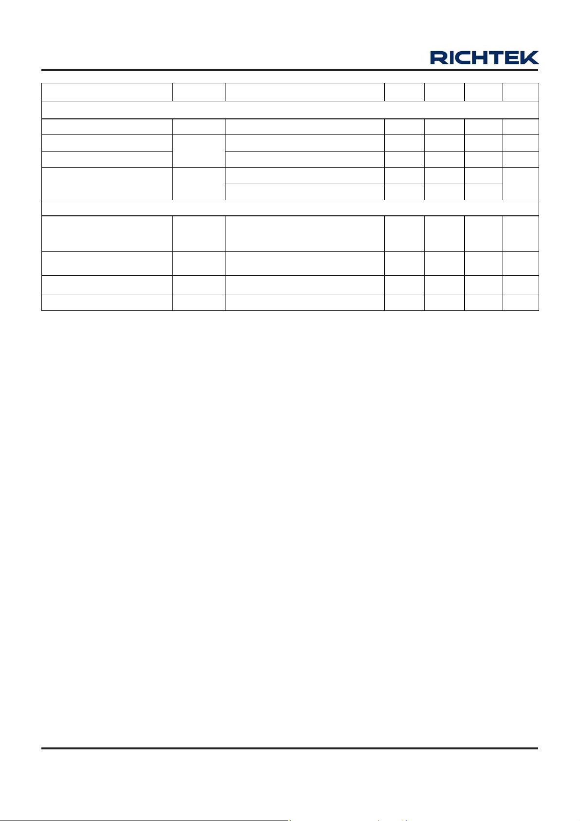
PWM Controller
Quiescent Supply Current VDD + VDDP, FB = 0.8V -- -- 1250 μA
TON Operating Current R
Shutdown Current I
4
DDP
= 5V, V
= 15V, V
IN
= 1.25V, EN/DEM = VDD, R
OUT
= 1MΩ, T
TON
= 25°C, unless otherwise specified)
A
Parameter Symbol Test Conditions Min Typ Max Unit
= 1M -- 15 -- μA
TON
VD D + VDDP - - 1 10 μA
TON -- 1 5 μA
SHDN
EN/DEM = 0V −10 −1 -- μA
To be continued
DS8202/A/B-05 April 2011www.richtek.com
Page 5
RT8202/A/B
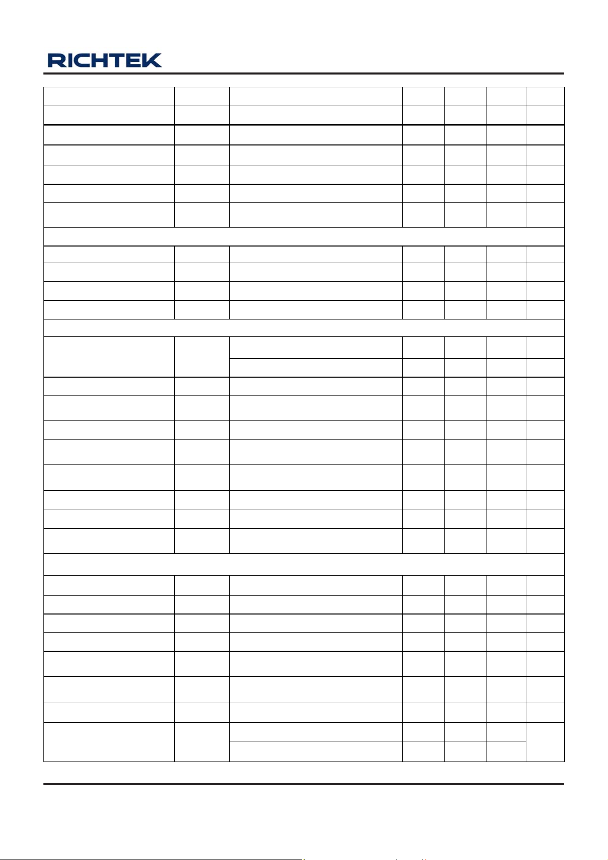
Parameter Symbol Test Conditions Min Typ Max Unit
FB Reference Voltage VFB V
= 4.5 to 5.5V 0.742 0.75 0.758 V
DD
FB Input Bias Curr ent FB = 0.75V −1 0.1 1 μA
Output Voltage Range V
On-Time VIN = 15V, V
0.75 -- 3.3 V
OUT
= 1.25V, R
OUT
= 1M 267 334 401 ns
TON
Minimum Off-Time 250 400 550 ns
V
Shutdown Discharge
OUT
Resistance
EN/DEM = GND -- 2 0 -- Ω
Current Sensing
ILI M Source Cur ren t LGATE = High 18 20 22 μA
Current Comparator Offset GND − OC −10 -- 10 mV
Cur ren t Limit Se tting Range R
2.5 -- 10 kΩ
ILIM
Zero Cro ss ing Thre shold GND − PHASE, EN/DEM = 5V −10 -- 5 mV
Fa ult Pr ot ec t i on
Cur ren t Limit Se nse
Voltage
V
RILIM
GND − PH ASE, R
GND − PH ASE, R
= 2.5k 35 50 65 mV
ILIM
= 10k 170 200 230 mV
ILIM
Output UV Threshold 60 70 80 %
OVP Threshold
W ith re spec t to erro r com para t or
threshold
10 15 20 %
OV Fault Delay FB forced above OV threshol d - - 20 -- μs
VDD UVLO Th re s hold
Soft-Start Ramp Time
Rising edge, Hysteresis = 20mV,
PWM disabled below this level
From EN high to internal V
REF
reac h
0.71V (0Æ95%)
4.1 4.3 4.5 V
-- 1.35 -- ms
UV Blank Time From EN signal going high -- 3.1 -- ms
Thermal Shutdown -- 155 -- °C
Thermal Shutdown
Hysteresis
-- 10 -- °C
Driver O n-Resi st ance
UG ATE Dr iv e r Pu ll Up BOOT − PHAS E = 5V -- 1.5 5 Ω
UG ATE Dr iv e r Si nk R
UGATEsk
BOOT − PH ASE = 5V -- 1. 5 5 Ω
LGATE Dri ver Pull Up LGATE, High St at e (S our ce) -- 1 .5 5 Ω
LGATE Dri ver Pull Down LGA TE , Low S tate (Sink) -- 0.6 2.5 Ω
UGATE Driver Source/Sink
Current
LGATE Dri ver Sour ce
Current
LGATE forced to 2.5V -- 1 -- A
UGATE − PH ASE = 2.5V,
BOOT − PHAS E = 5V
-- 1 -- A
LGATE Dri ver Sink Curr ent LGA TE forc ed to 2.5V -- 3 -- A
LGATE Rising (PHASE = 1.5V) -- 30 - -
Dead Time
ns
UGATE Ris ing -- 30 --
To be continued
DS8202/A/B-05 April 2011 www.richtek.com
5
Page 6
RT8202/A/B
Parameter Symbol Test Conditions Min Typ Max Unit
Logic I/O
EN/DE M Logic Low V oltage -- -- 0.8 V
EN/DE M Logic Hig h Voltage 2.9 -- -- V
EN/DE M Float ing V oltage
Logic In put Cur rent
EN/D EM Open -- 2 - - V
EN/DEM = VDD -- 1 5
μA
EN/DEM = 0 −5 −1 --
PGO OD (u pper side thresh ol d de ci de by OV th reshold)
Measured at FB, with respect to
Trip Thr eshold (Falli ng)
reference, no load.
−13 −10 −7 %
Hysteresis = 3%
Fault Propagation Delay
Output Low Voltage I
Falling edge, FB forced below
PGOOD trip threshold
= 1mA -- -- 0.4 V
SINK
-- 2.5 -- μs
Leakage Current High state, forced to 5.0V -- -- 1 μA
Note 1. Stresses listed as the above “Absolute Maximum Ratings” may cause permanent damage to the device. These are for
stress ratings. Functional operation of the device at these or any other conditions beyond those indicated in the
operational sections of the specifications is not implied. Exposure to absolute maximum rating conditions for extended
periods may remain possibility to affect device reliability.
Note 2. θ
Note 3. Devices are ESD sensitive. Handling precaution is recommended.
Note 4. The device is not guaranteed to function outside its operating conditions.
is measured in the natural convection at TA = 25°C on a high effective four layers thermal conductivity test board of
JA
JEDEC 51-7 thermal measurement standard. The case point of θ
is on the expose pad of the package.
JC
DS8202/A/B-05 April 2011www.richtek.com
6
Page 7
Typical Operating Characteristics
RT8202/A/B
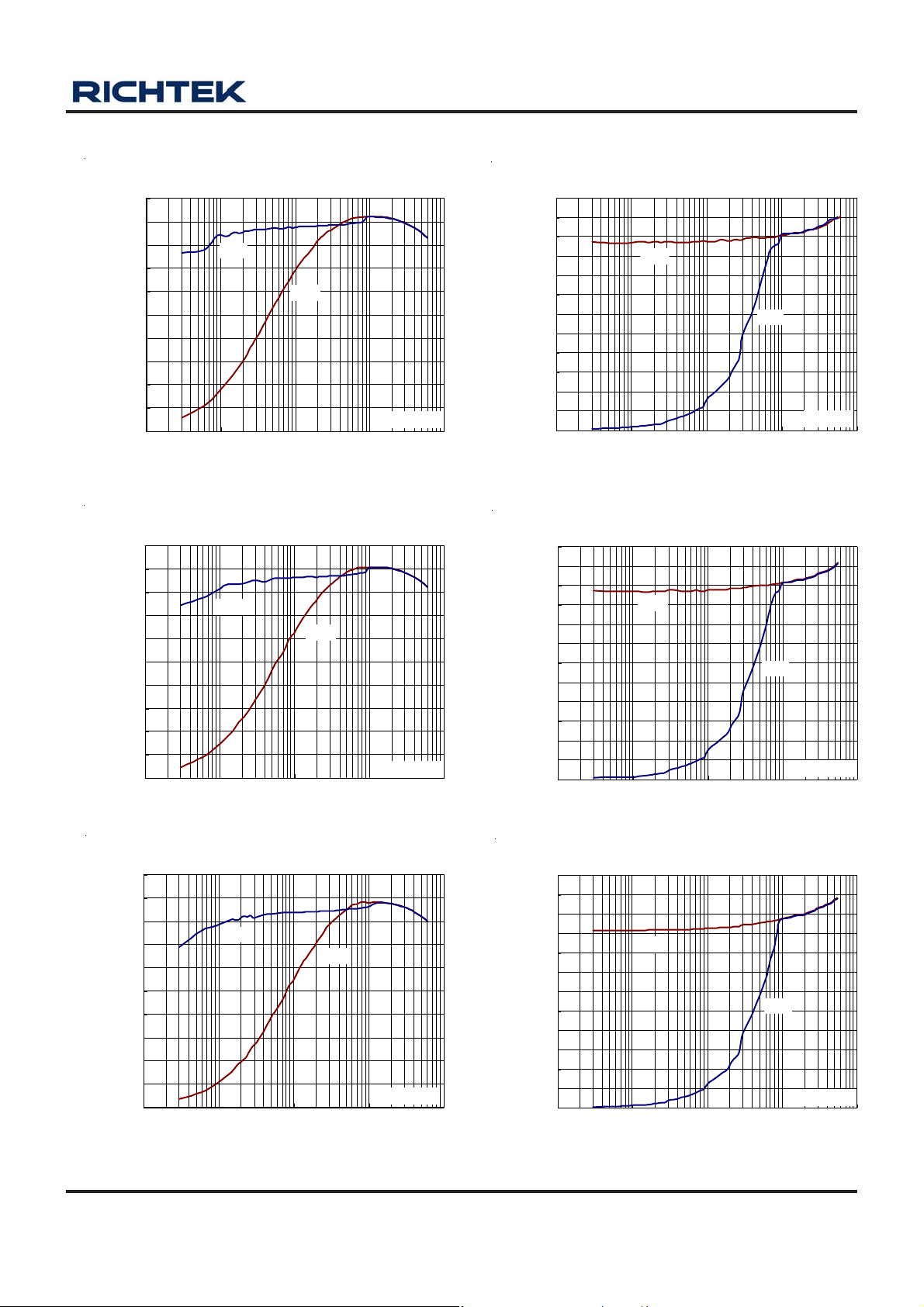
Efficiency vs. Output Current
100
90
80
70
60
50
40
Eff iciency ( % )
30
20
10
0
0.001 0.01 0.1 1 10
DEM
PWM
Output Current (A)
Efficiency vs. Output Current
100
90
80
70
60
50
40
Efficiency (%)
30
20
10
0
0.001 0.01 0.1 1 10
DEM
PWM
VIN = 12V
Output Current (A)
VIN = 8V
Switching Frequency vs. Output Current
300
275
250
225
200
175
150
125
100
75
50
Swit ching Frequency (kHz)
25
0
0.001 0.01 0.1 1 10
PWM
DEM
Output Current (A)
Switching Frequency vs. Output Current
300
275
250
225
200
175
150
125
100
75
50
Swit ching Frequency (kHz)
25
0
0.001 0.01 0.1 1 10
PWM
DEM
Output Current (A)
VIN = 8V
VIN = 12V
Efficiency vs. Output Current
100
90
80
70
60
50
40
Efficiency (%)
30
20
10
0
0.001 0.01 0.1 1 10
DEM
PWM
VIN = 24V
Output Current (A)
Switching Frequency vs. Output Current
300
275
250
225
200
175
150
125
100
75
50
Switching Frequency (kHz)
25
0
0.001 0.01 0.1 1 10
PWM
DEM
Output Current (A)
VIN = 24V
DS8202/A/B-05 April 2011 www.richtek.com
7
Page 8
RT8202/A/B
400
390
380
370
360
350
340
330
320
310
Standby Cur rent (uA)
300
290
280
V
OUT
(1V/Div)
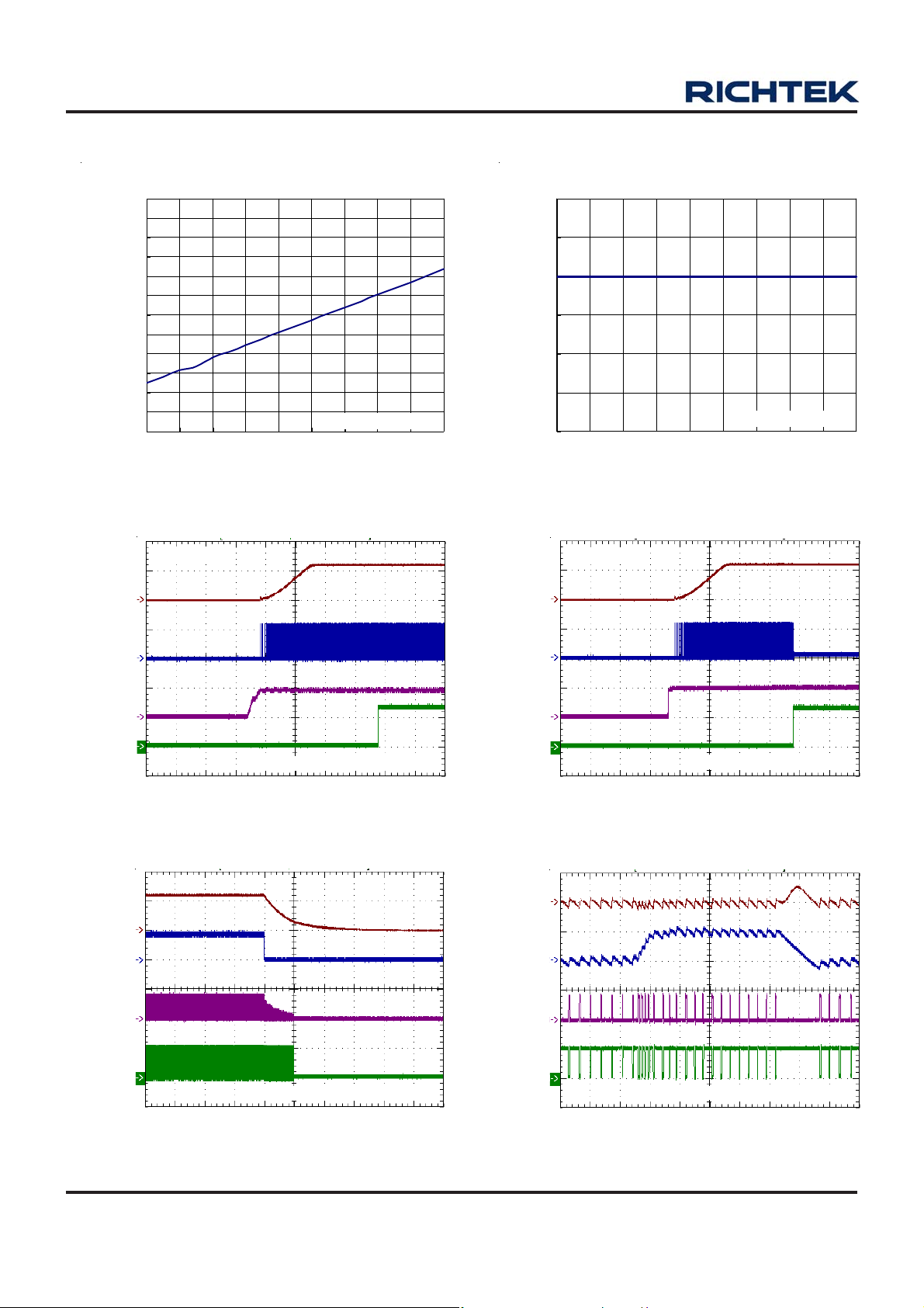
Standby Current vs. Input Voltage
EN = 5V, No Loa d
7 9 11 13 15 17 19 21 23 25
Input Volt age (V)
Power On from EN
PWM-Mode
3.0
2.5
2.0
1.5
1.0
Shutdown Current (uA)
0.5
0.0
V
OUT
(1V/Div)
Shutdown Current vs. Input Voltage
EN = GND, No Load
7 9 11 13 15 17 19 21 23 25
Inpu t Voltage (V)
Power On from EN
DEM-Mode
PHASE
(10V/Div)
EN/DEM
(2V/Div)
PGOOD
(2V/Div)
V
OUT
(1V/Div)
EN/DEM
(2V/Div)
UGATE
(20V/Div)
LGATE
(5V/Div)
V
= 12V, EN = Floating, No Load
IN
Time (800μs/Div)
Power Off from EN
V
= 12V, EN = Floating, No Load
IN
PHASE
(10V/Div)
EN/DEM
(5V/Div)
PGOOD
(2V/Div)
V
OUT_ac
(100mV/Div)
I
LOAD
(5A/Div)
UGATE
(20V/Div)
LGATE
(5V/Div)
V
= 12V, EN = 5V, No Load
IN
Time (800μs/Div)
V
Load Transient Response
OUT
V
= 12V, EN = Floating, I
IN
= 0A to 6A
OUT
Time (4ms/Div)
Time (10μs/Div)
DS8202/A/B-05 April 2011www.richtek.com
8
Page 9
RT8202/A/B
V
OUT
(1V/Div)
UGATE
(10V/Div)
LGATE
(5V/Div)
V
OUT
(1V/Div)
I
LOAD
(10A/Div)
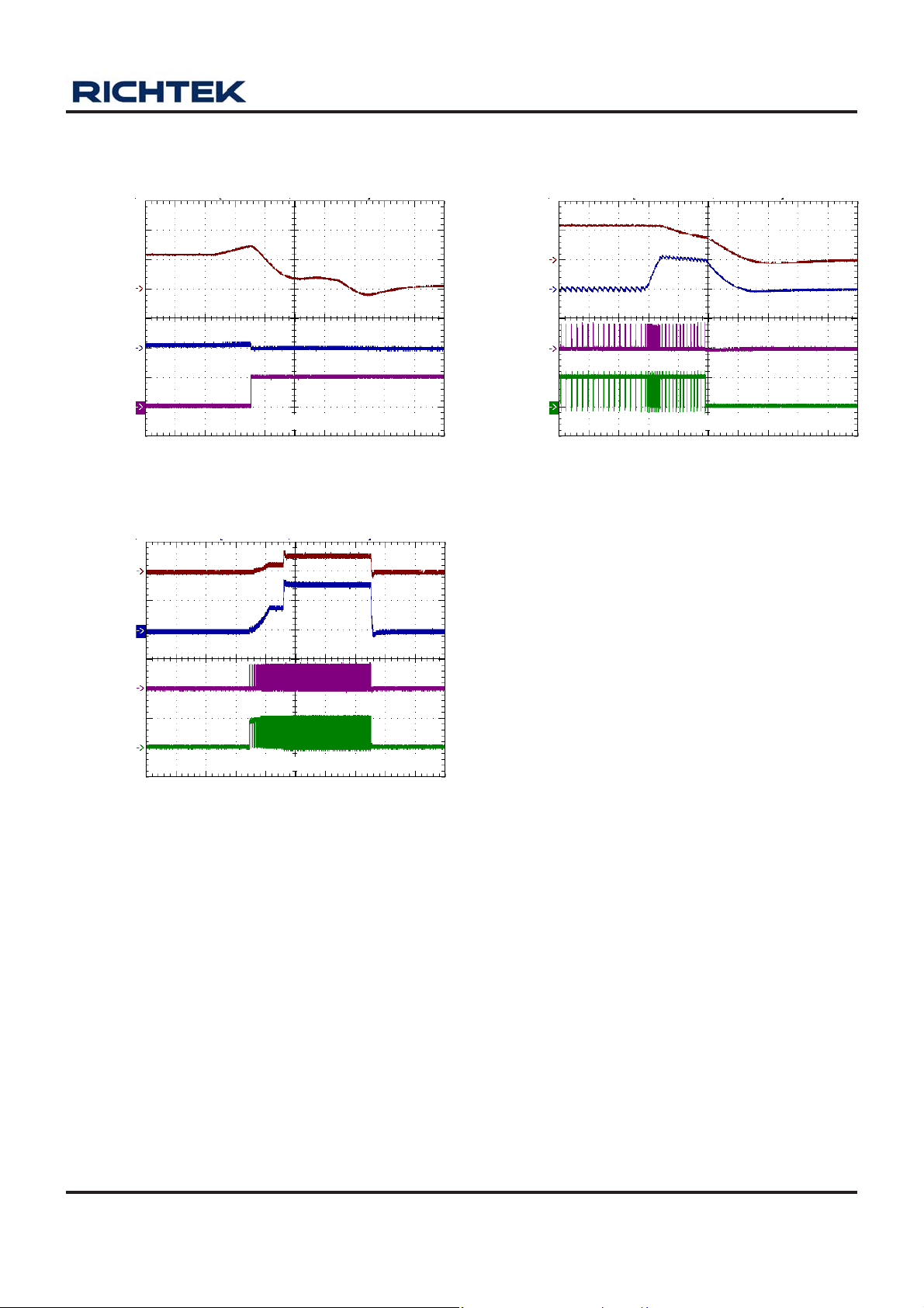
OVP
V
= 12V, EN = 5V, No Load
IN
Time (40μs/Div)
Power On in Short Condition
V
OUT
(1V/Div)
I
LOAD
(20A/Div)
UGATE
(20V/Div)
LGATE
(5V/Div)
UVP
V
= 12V, EN = Floating, No Load
IN
Time (20μs/Div)
UGATE
(20V/Div)
LGATE
(5V/Div)
V
= 12V, EN = Floating, V
IN
Time (800μs/Div)
OUT
Short
DS8202/A/B-05 April 2011 www.richtek.com
9
Page 10

RT8202/A/B
Application Information
The RT8202/A/B PWM controller provides high efficiency ,
excellent transient response, a nd high DC output a ccuracy
needed for stepping down high voltage batteries to
generate low voltage CPU core, I/O, and chipset RAM
supplies in notebook computers. Richtek Mach
ResponseTM technology is specifically designed for
providing 100ns “instant-on” response to load steps while
maintaining a relatively constant operating frequency a nd
inductor operating point over a wide range of input voltages.
The topology circumvents the poor load transient timing
problems of fixed-frequency current mode PWMs while
avoiding the problems caused by widely varying switching
frequencies in conventional constant-on-ti me and constantoff-time PWM schemes. The DRVTM mode PWM
modulator is specifically designed to have better noise
immunity for such a single output application.
PWM Operation
The Mach Response
TM
DRVTM mode controller relies on
,
the output filter capacitor's effective series resistance
(ESR) to act as a current sense resistor, so the output
ripple voltage provides the PWM ra mp signal. Refer to the
function diagra ms of RT8202/A/B, the synchronous high
side MOSFET is turned on at the beginning of each cycle.
After the internal one-shot timer expires, the MOSFET is
turned off. The pulse width of this one shot is determined
by the converter's input and output voltages to keep the
frequency fairly constant over the input voltage range.
Another one-shot sets a minimum off-time (400ns typ.).
On-Time Control (TON)
The on-time one-shot comparator has two inputs. One
input monitors the output voltage, while the other input
samples the input voltage and converts it to a current.
This input voltage proportional current is used to charge
an internal on-time capacitor. The on-time is the time
required for the voltage on this capacitor to charge from
zero volts to V
, thereby making the on-time of the high
OUT
side switch directly proportional to output voltage and
inversely proportional to input voltage. The implementation
results in a nearly constant switching frequency without
the need a clock generator.
And then the switching frequency is :
Frequency = V
R
is a resistor connected from the input supply (VIN)
TON
/ (VIN x TON)
OUT
to TON pin.
Mode Selection (EN/DEM) Operation
The EN/DEM pin enables the supply. When EN/DEM is
tied to VDD, the controller is enabled and operates in
diode-emulation mode. When the EN/DEM pin is floating,
the RT8202/A/B will operate in forced-CCM mode.
Diode-Emulation Mode (EN/DEM = High)
In diode-emulation mode, RT8202/A/B automatically
reduces switching frequency at light-load conditions to
maintain high efficiency. This reduction of frequency is
achieved smoothly a nd without increasing V
ripple or
OUT
load regulation. As the output current decreases from
heavy-load condition, the inductor current is also reduced,
and eventually comes to the point that its valley touches
zero current, which is the boundary between continuous
conduction and discontinuous conduction modes. By
emulation the behavior of diodes, the low-side MOSFET
allows only partial of negative current when the inductor
freewheeling current reach negative. As the loa d current
is further decrea sed, it takes longer and longer to discharge
the output capacitor to the level than requires the next
“ON” cycle. The on-time is kept the same as that in the
heavy-load condition. In reverse, when the output current
increases from light load to heavy load, the switching
frequency increases to the preset value as the inductor
current reaches the continuous condition. The tra n sition
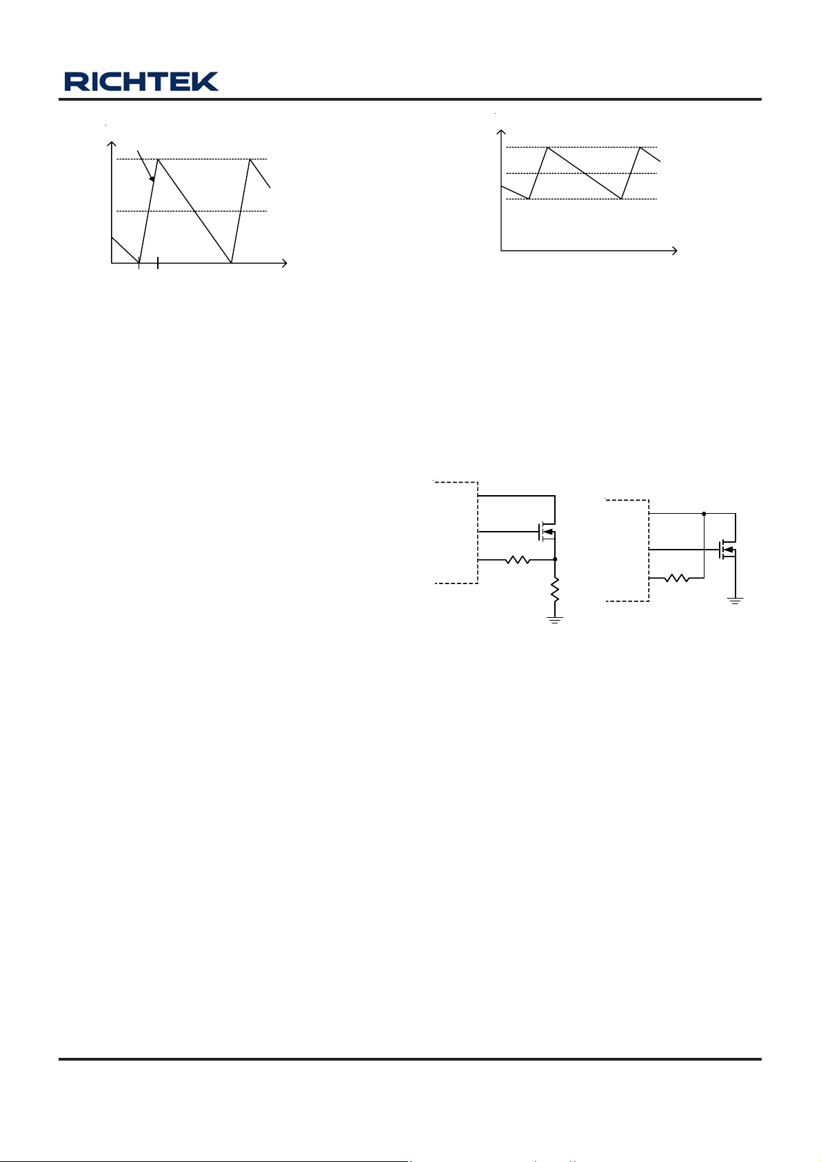
load point to the light load operation ca n be calculated as
follows (Figure 1) :
(V V )
−
IT
LOAD ON
IN OUT
≈×
2L
where TON is On-time.
TON = 3.85p x R
10
TON
x V
OUT
/ (V
IN
− 0.5)
DS8202/A/B-05 April 2011www.richtek.com
Page 11
I
L
Slope = (VIN -V
OUT
) / L
i
L, peak
i
Load
= i
L, peak
/ 2
RT8202/A/B
I
L
I
L, peak
I
Load
I
LIM
0
t
ON
t
Figure 1. Boundary condition of CCM/DEM
The switching waveforms may appear noisy and
asynchronous when light loa ding causes diode-emulation
operation, but this is a normal operating condition that
results in high light-load efficiency . T rade-offs in DEM noise
vs. light-load efficiency are made by varying the inductor
value. Generally, low inductor values produce a broader
efficiency vs. load curve, while higher values result in higher
full-load efficiency (assuming that the coil resistance
remains fixed) and less output voltage ripple. The
disadvantages for using higher inductor values include
larger physical size and degrades loa d-transient response
(especially at low input voltage levels).
Forced-CCM Mode (EN/DEM = floating)
The low noise, forced-CCM mode (EN/DEM = floating)
disables the zero-crossing comparator, which controls the
low-side switch on-time. This causes the low side gatedrive waveform to become the complement of the high
side gate-drive waveform. This in turn causes the inductor
current to reverse at light loads as the PWM loop to
maintain a duty ratio V
OUT/VIN
. The benefit of forced-CCM
mode is to keep the switching frequency fairly constant,
but it comes at a cost : The no-load battery current can
be up to 10mA to 40mA, depending on the external
MOSFETs.
Current Limit Setting (OCP)
RT8202/A/B has cycle-by-cycle current limiting control.
The current limit circuit employs a unique “valley” current
sensing algorithm. If the magnitude of the current-sense
signal at OC is above the current limit threshold, the PWM
is not allowed to initiate a new cycle (Figure 2).
0
t
Figure 2. V alley Current-Limit
Current sensing of the RT8202/A/B can be a ccomplished
in two ways. Users can either use a current sense resistor
or the on-state of the low side MOSFET (R
DS(ON)
). For
resistor sensing, a sense resistor is pla ced between the
source of low-side MOSFET and PGND (Figure 3(a)).
R
sensing is more efficient a nd less expensive (Figure
DS(ON)
3(b)). There is a compromise between current-limit
accura cy a nd sense re sistor power dissipation.
PHASE
PHASE
LGATE
OC
R
ILIM
LGATE
OC
R
ILIM
(a) (b)
Figure 3. Current-Sense Methods
In both case s, the R
resistor between the OC pin and
ILIM
PHASE pin sets the over current threshold. This resistor
R
is connected to a 20μA current source within the
ILIM
RT8202/A/B which is turned on when the low side
MOSFET turns on. When the voltage drop across the
sense resistor or low side MOSFET equals the voltage
across the R
resistor, positive current li mit will activate.
ILIM
The high side MOSFET will not be turned on until the
voltage drop across the sense element (resistor or
MOSFET) falls below the voltage across the R
resistor.
ILIM
Choose a current limit resistor by following Equation :
R
= I
ILIM
x R
LIMIT
SENSE
/ 20μA
Carefully observe the PC board layout guidelines to ensure
that noise and DC errors do not corrupt the current-sense
signal seen by OC and PGND. Mount the IC close to the
low-side MOSFET and sense resistor with short, direct
DS8202/A/B-05 April 2011 www.richtek.com
11
Page 12
RT8202/A/B
traces, making a Kelvin sense connection to the sense
resistor.
MOSFET Gate Driver (UGATE, LGA TE)
The high side driver is designed to drive high current, low
R
N-MOSFET(s). When configured as a floating
DS(ON)
driver, 5V bia s voltage is delivered from V DDP supply . The
average drive current is proportional to the gate charge at
VGS = 5V times switching frequency. The instantaneous
drive current is supplied by the flying capacitor between
BOOT and PHASE pins.
A dead time to prevent shoot through is internally
generated between high side MOSFET off to low side
MOSFET on, and low side MOSFET off to high side
MOSFET on.
The low side driver is designed to drive high current, low
R
N-MOSFET(s). The internal pull-down tra nsistor
DS(ON)
that drives LGATE low is robust, with a 0.6Ω typical on-
resistance. A 5V bias voltage is delivered form VDDP
supply . The instanta neous drive current is supplied by the
flying capa citor between V DDP and PGND.
For high current application s, some combinations of high
and low side MOSFETs might be encountered that will
cause excessive gate-drain coupling, which can lead to
efficiency killing, EMI producing shoot through currents.
This is often remedied by adding a resistor in series with
BOOT, which increa ses the turn-on ti me of the high side
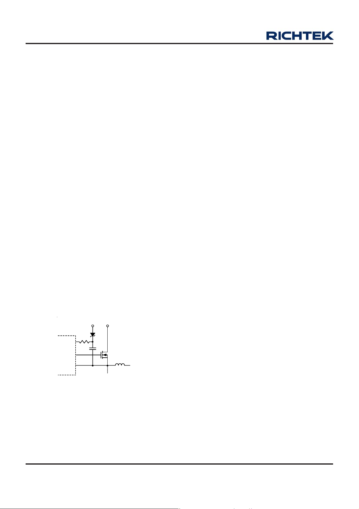
MOSFET without degrading the turn-off time (Figure 4).
V
IN
+5V
BOOT
UGATE
PHASE
R
Figure 4. Reducing the UGA TE Rise T ime
Power Good Output (PGOOD)
The power good output is an open-drain output and requires
a pull up resistor. When the output voltage is 15% a bove
or 10% below its set voltage, PGOOD gets pulled low. It
is held low until the output voltage returns to within these
tolerances once more. In soft start, PGOOD is actively
held low and is allowed to tra nsition high until soft start is
over and the output rea ches 93% of its set voltage. There
is a 2.5μs delay built into PGOOD circuitry to prevent
false transition.
POR, UVLO and Soft-Start
Power on reset (POR) occurs when VDD rises a bove to
approximately 4.3V, the RT8202/A/B will reset the fault
latch and preparing the PWM for operation. Below
4.1V
, the V DD under voltage-lockout (UVLO) circuitry
(MIN)
inhibits switching by keeping UGA TE and LGATE low .
A built-in soft-start is used to prevent surge current from
power supply input after EN/DEM is enabled. It clamps
the ramping of intern al reference voltage which is compared
with FB signal. The typical soft-start duration is 1.35ms.
Furthermore, the maximum allowed current limit is
segment in 2 steps during 1.35ms period.
Output Over Voltage Protection (OVP)
The output voltage can be continuously monitored for over
voltage protection. When the output voltage exceeds 15%
of the its set voltage threshold, over voltage protection is
triggered and the low side MOSFET is latched on. This
activates the low side MOSFET to discharge the output
ca p acitor.
RT8202/A/B is latched once OVP is triggered and can
only be relea sed by V DD or EN/DEM power on reset. There
is 20us delay built into the over voltage protection circuit
to prevent false transitions.
Output Under Voltage Protection (UVP)
The output voltage can be continuously monitored for under
voltage protection. When the output voltage is less than
70% of its set voltage threshold, under voltage protection
is triggered and then both UGA TE and LGA TE gate drivers
are forced low . In order to remove the residual charge on
the output capacitor during the under voltage period, if
PHASE is greater than 1V, the LGA TE is forced high until
PHASE is lower than 1V. There is 2.5us delay built into
the under voltage protection circuit to prevent false
transitions. During soft-start, the UVP will be blanked
around 3.1ms.
12
DS8202/A/B-05 April 2011www.richtek.com
Page 13
)
Output V oltage Setting (FB)
RT8202/A/B
V
IN
The output voltage can be adjusted from 0.75V to 3.3V by
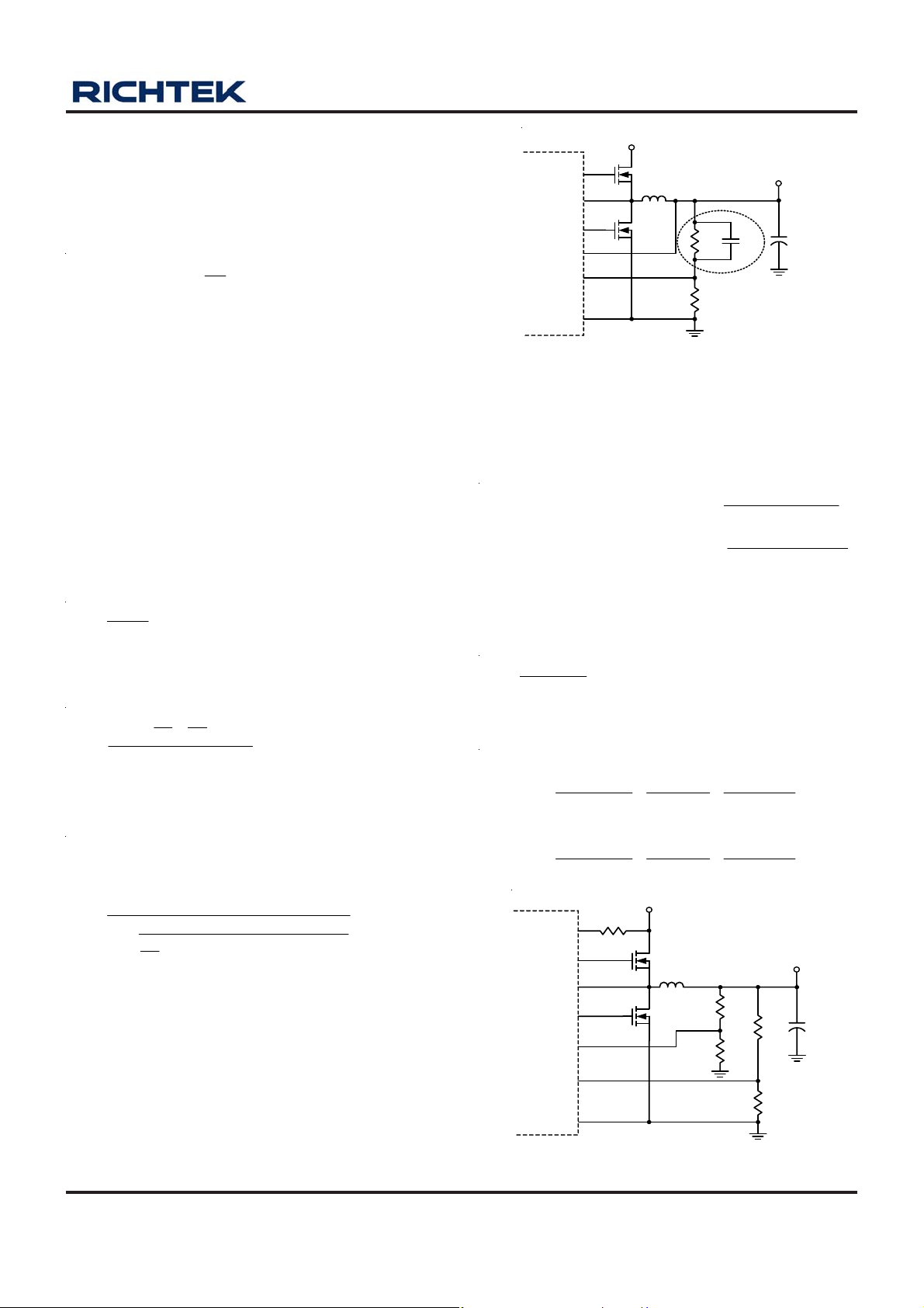
setting the feedback resistor R1 a nd R2 (Figure 5). Choose
R2 to be approxi mately 10kΩ, and solve f or R1 using the
equation:
⎡⎤
R1
V = V 1
OUT FB
⎛⎞
×+
⎜⎟
⎢⎥
R2
⎝⎠
⎣⎦
where VFB is 0.75V.
Note that in order for the device to regulate in a controlled
manner , the ripple content at the feedba ck pin, VFB, should
be approxi mately 15mV at minimum V
no smaller than 10mV. If V
at minimum V
ripple
, and worst ca se
BAT
BAT
is less
than 15mV, the above component values should be
revisited in order to improve this. Quite often a small
cap acitor , C1, is required in parallel with the top feedbac k
resistor, R1, in order to ensure that VFB is large enough.
The value of C1 can be calculated a s follows, where R2 is
the bottom feedback resistor .
Firstly calculating the value of Z1 required :
Z1 = V 0.015
R2
×−Ω
()
0.015
ripple_VBAT(MIN)
C1
Z1
V
OUT
C2
UGATE
PHASE
BOOT
VOUT
FB
GND
R1
R2
Figure 5. Setting The Output Voltage
For application that output voltage is higher than 3.3V,
user can also use a voltage divider to keep VOUT pin
voltage within 0.75V to 2.8V as shown in Figure 6. For
this case, T
If R < 2M then T = 3.85p
TON ON
If R 2M then T = 3.55p
TON ON
Where R
can be determined as below :
ON
×
RV
Ω×
≥Ω ×
is TON set resistor and the V
TON
TON OUT_FB
V0.5
IN
R V
TON OUT_FB
V0.4
IN
−
×
−
OUT_FB
is the
output signal of resistor divider. Since the switching
frequency is
Secondly calculating the value of C1 required to achieve
F =
S
this :
11
−
(
C1 = F
Z1 R1
2f
××
π
SW_VBAT(MIN)
Finally using the equation a s follows to verify the value of
V
:
FB
V = V
FB_VBAT(MIN) ripple_VBAT(MIN)
For a given switching frequency , we can obtain the R
a s below
If R < 2M then
TON
R =
TON
If R 2M then
TON
R =
TON
⎡⎤
⎢⎥
⎢⎥
V
×
⎢⎥
R2+
⎢⎥
1
⎢⎥
⎣⎦
where V
minimum V
f
sw_VBAT(MIN)
V
FB_VBAT(MIN)
V
.
BAT
+×× ×
R1
ripple_VBAT(MIN)
;
BAT
is the switching frequency in minimum V
is the ripple voltage into FB pin in minimum
R2
1
2f C1
π
SW_VBAT(MIN)
is the output ripple voltage in
BAT
;
V
OUT
VT×
IN ON
Ω
−
V0.5V
OUT OUT
V V F 3.85p
IN OUT_FB S
≥Ω
−
V0.4V
OUT OUT
V V F 3.55p
IN OUT_FB S
R
VIN
UGATE
PHASE
BOOT
VOUT
FB
GND
TON
××
××
V
IN
V
OUT_FB
1
×
1
×
R3
R1
R4
R2
TON
V
OUT
C2
Figure 6. Output Voltage Setting for V
OUT
> 3.3V
Application
DS8202/A/B-05 April 2011 www.richtek.com
13
Page 14

RT8202/A/B
Output Inductor Selection
The switching frequency (on-time) and operating point (%
ripple or LIR) determine the inductor value as f ollows :
T(V - V)
×
ON IN OUT
L =
LI
×
IR LOAD(MAX)
Find a low pass inductor having the lowest possible DC
resistance that fits in the allowed dimen sions. Ferrite cores
are often the best choice, although powdered iron is
inexpensive and ca n work well at 200kHz. The core must
be large enough and not to saturate at the pea k inductor
current (I
I
= I
PEAK
) :
PEAK
LOAD(MAX)
+ [(LIR / 2) x I
LOAD(MAX)
]
Output Capacitor Selection
The output filter ca pacitor must have ESR low enough to
meet output ripple and loa d transient requirement, yet have
high enough ESR to satisfy stability requirements. Also,
the cap acitance value must be high enough to a bsorb the
inductor energy going from a full load to no load condition
without tripping the OVP circuit.
Do not put high value ceramic capacitors dire ctly across
the outputs without taking precautions to ensure sta bility .
Large ceramic capacitors can have a high ESR zero
frequency and cause erratic and unstable operation.
However, it is easy to add sufficient series resistance by
placing the ca pacitors a couple of inche s downstream from
the inductor and connecting V
or FB divider close to
OUT
the inductor.
There are two related but distinct ways including double
pulsing and feedback loop instability to identify the
unstable operation.
Double-pulsing occurs due to noise on the output or
because the ESR is too low that there is not enough
voltage ramp in the output voltage sign al. The “fools” the
error comparator into triggering a new cycle immediately
after 400ns minimum off-time period ha s expired. Doublepulsing is more annoying tha n harmful, resulting in nothing
worse than increased output ripple. However, it may
indicate the possible presence of loop instability, which
is caused by insufficient ESR.
For CPU core voltage converters and other applications
where the output is subject to violent load transient, the
output capacitor's size depends on how much ESR is
needed to prevent the output from dipping too low under a
load transient. Ignoring the sag due to f inite cap acita nce :
V
ESR
≤
P-P
I
LOAD(MAX)
In non-CPU applications, the output capacitor's size
depends on how much ESR is needed to maintain at an
accepta ble level of output voltage ripple :
V
ESR
≤
LI
P-P
×
IR LOAD(MAX)
Organic semiconductor ca pa citor(s) or specially polymer
cap acitor(s) are recommended.
Output Capacitor Stability
Stability is determined by the value of the ESR zero relative
to the switching frequency . The point of instability is given
by the following equation :
f =
ESR
1
2 ESR C 4
π
×× ×
OUT
f
SW
≤
Loop instability ca n result in oscillation at the output after
line or load perturbations that can trip the over voltage
protection latch or cause the output voltage to fall below
the tolerance limit.
The easiest method for stability checking is to apply a
very zero-to-max load tran sient and carefully observe the
output-voltage-ripple envelope for overshoot a nd ringing. It
helps to simultaneously monitor the inductor current with
AC probe. Do not allow more tha n one ringing cycle after
the initial step-response under- or over-shoot.
Thermal Considerations
For continuous operation, do not exceed absolute
maximum operation junction temperature.
The maximum power dissipation depends on the thermal
resistance of IC package, PCB layout, the rate of
surroundings airflow and temperature difference between
junction to ambient. The maximum power dissipation ca n
be calculated by following formula :
P
Where T
temperature 125°C, T
θ
= ( T
D(MAX)
J(MAX)
is the junction to ambient thermal resistance.
JA
- TA ) / θ
J(MAX)
JA
is the maximum operation junction
is the ambient temperature a nd the
A
14
DS8202/A/B-05 April 2011www.richtek.com
Page 15
RT8202/A/B
For recommended operating conditions specification of
RT8202/A/B, where T
is the maximum junction
J(MAX)
temperature of the die (125°C) and TA is the maximum
ambient temperature. The junction to ambient thermal
resistance θ
is layout dependent. For WQFN-16L 3x3
JA
packages, the thermal resistance θJA is 68°C/W on the
standard JEDEC 51-7 four layers thermal test board. For
WQFN-14L 3.5x3.5 pack age, the thermal resistance θ
JA
is 60°C/W on the standard JEDEC 51-7 f our layers thermal
test board. The maximum power dissipation at TA = 25°C
can be calculated by following f ormula :
P
= (125°C − 2°C) / (68°C/W) = 1.471W for
D(MAX)
WQF N-16L 3x3 pa ckages
P
= (125°C − 25°C) / (54°C/W) = 1.852W for
D(MAX)
WQF N-16L 4x4 pa ckages
P
= (125°C − 25°C) / (60°C/W) = 1.667W for
D(MAX)
WQF N-14L 3.5x3.5 packages
The maximum power dissipation depends on operating
ambient temperature for fixed T
and thermal
J(MAX)
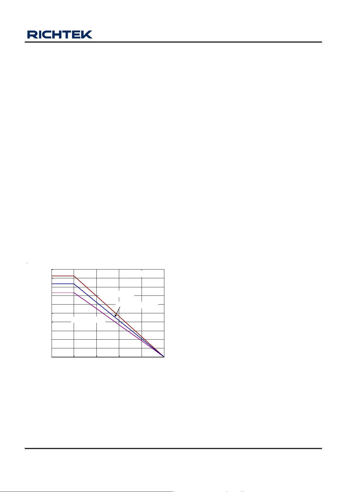
resistance θJA. For RT8202/A/B packages, the Figure 7
of derating curves allows the designer to see the effect of
rising ambient temperature on the maximum power
allowed.
2.0
1.8
1.6
1.4
1.2
1.0
0.8
0.6
0.4
0.2
Maximum Power Dissipation (W)
0.0
0 25 50 75 100 125
WQFN -16L 3x3
WQFN -16L 4x4
Ambient Temperature (°C)
Four Layer PCB
WQFN -14L 3.5x3.5
Layout Considerations
Layout is very important in high frequency switching
converter design. If designed improperly , the PCB could
radiate excessive noise and contribute to the converter
instability. Certain points must be considered before
starting a layout for RT8202/A/B.
` Connect RC low pa ss filter from V DDP to V DD, 1uF a nd
10Ω are recommended. Place the filter ca pa citor close
to the IC.
` Keep current limit setting network a s close a s possible
to the IC. Routing of the network should avoid coupling
to high voltage switching node.
` Connections from the drivers to the respective gate of
the high side or the low side MOSFET should be as
short as possible to reduce stray inductance.
` All sensitive analog traces and components such as
VOUT, FB, GND, EN/DEM, PGOOD, OC, VDD, and
TON should be placed away from high voltage switching
nodes such as PHASE, LGATE, UGATE, or BOOT
nodes to avoid coupling. Use internal layer(s) a s ground
plane(s) and shield the feedba ck trace from power tra ces
and components.
` Current sense connections must always be made using
Kelvin connections to ensure an accurate signal, with
the current limit resistor located at the device.
` Power sections should connect directly to ground
plane(s) using multiple vias as required for current
handling (including the chip power ground connection s).
Power components should be placed to minimize loops
and reduce losses.
Figure 7. Derating Curves f or RT8202/A/B Pack ages
DS8202/A/B-05 April 2011 www.richtek.com
15
Page 16
RT8202/A/B
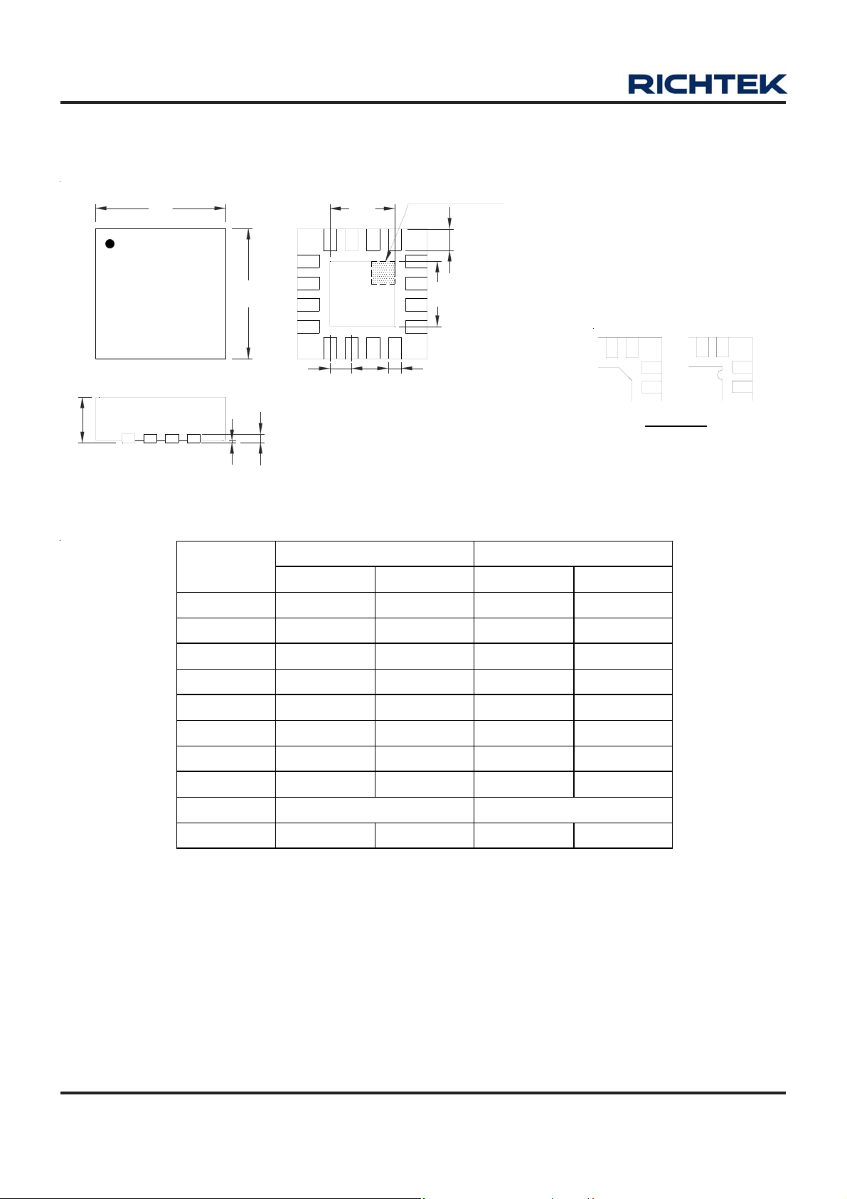
Outline Dimension
D
E
A
A3
A1
D2
e
SEE DETAIL A
1
E2
b
L
1
2
1
2
DETAIL A
Pin #1 ID a nd T ie Bar Mark Option s
Note : The configuration of the Pin #1 identifier is optional,
but must be located within the zone indicated.
Dimensions In Millimeters Dimensions In Inches
Symbol
Min Max Min Max
A 0.700 0.800 0.028 0.031
A1 0.000 0.050 0.000 0.002
A3 0.175 0.250 0.007 0.010
b 0.180 0.300 0.007 0.012
D 2.950 3.050 0.116 0.120
D2 1.300 1.750 0.051 0.069
E 2.950 3.050 0.116 0.120
E2 1.300 1.750 0.051 0.069
e 0.500 0.020
L 0.350 0.450
0.014 0.018
W-Type 16L QFN 3x3 Package
16
DS8202/A/B-05 April 2011www.richtek.com
Page 17
RT8202/A/B
D
E
A
A3
A1
D2
e
SEE DETAIL A
1
E2
b
L
1
2
1
2
DETAIL A
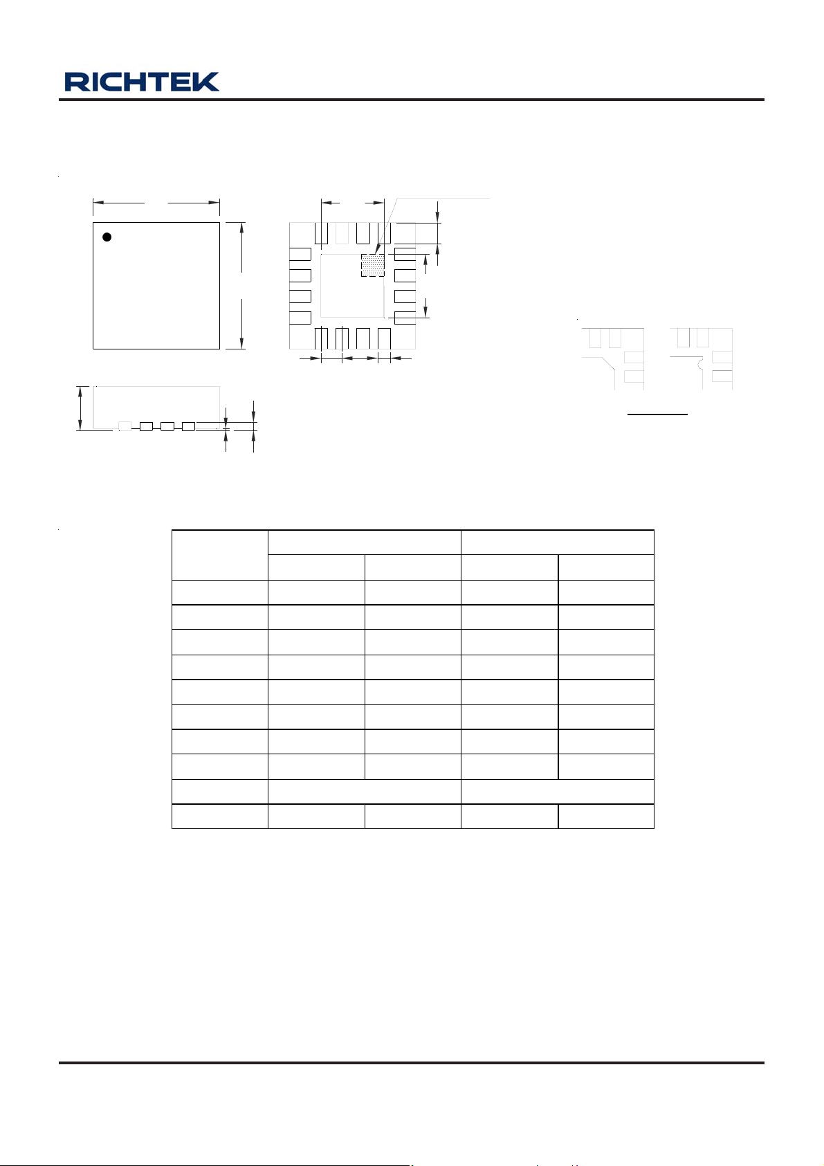
Pin #1 ID a nd T ie Bar Mark Option s
Note : The configuration of the Pin #1 identifier is optional,
but must be located within the zone indicated.
Dimensions In Millimeters Dimensions In Inches
Symbol
Min Max Min Max
A 0.700 0.800 0.028 0.031
A1 0.000 0.050 0.000 0.002
A3 0.175 0.250 0.007 0.010
b 0.250 0.380 0.010 0.015
D 3.950 4.050 0.156 0.159
D2 2.000 2.450 0.079 0.096
E 3.950 4.050 0.156 0.159
E2 2.000 2.450 0.079 0.096
e 0.650 0.026
L 0.500 0.600
0.020 0.024
W-Type 16L QFN 4x4 Package
DS8202/A/B-05 April 2011 www.richtek.com
17
Page 18
RT8202/A/B
2
DETAIL A
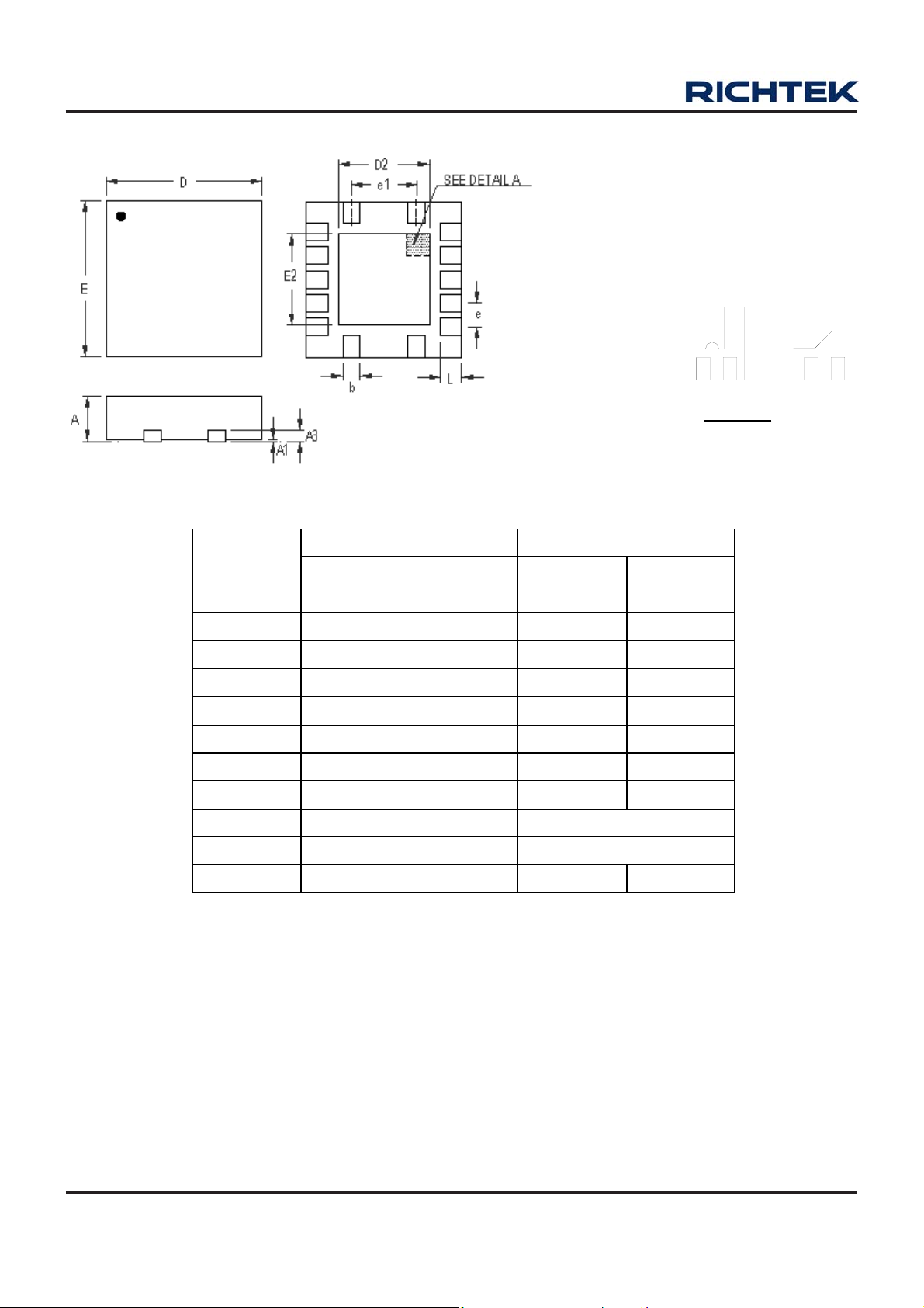
Pin #1 ID a nd T ie Bar Mark Option s
Note : The configuration of the Pin #1 identifier is optional,
but must be located within the zone indicated.
Dimensions In Millimeters Dimensions In Inches
Symbol
Min Max Min Max
A 0.700 0.800 0.028 0.031
A1 0.000 0.050 0.000 0.002
A3 0.175 0.250 0.007 0.010
b 0.180 0.300 0.007 0.012
D 3.400 3.600 0.134 0.142
D2 1.950 2.150 0.077 0.085
E 3.400 3.600 0.134 0.142
E2 1.950 2.150 0.077 0.085
1
1
2
e 0.500 0.020
e1 1.500 0.060
L 0.300 0.500
0.012 0.020
W-Type 14L QFN 3.5x3.5 Package
Richtek Technology Corporation
Headquarter
5F, No. 20, Taiyuen Street, Chupei City
Hsinchu, Taiwan, R.O.C.
Tel: (8863)5526789 Fax: (8863)5526611
Information that is provided by Richtek Technology Corporation is believed to be accurate and reliable. Richtek reserves the right to make any change in circuit
design, specification or other related things if necessary without notice at any time. No third party intellectual property infringement of the applications should be
guaranteed by users when integrating Richtek products into any application. No legal responsibility for any said applications is assumed by Richtek.
18
Richtek Technology Corporation
Taipei Office (Marketing)
5F, No. 95, Minchiuan Road, Hsintien City
Taipei County, Taiwan, R.O.C.
Tel: (8862)86672399 Fax: (8862)86672377
Email: [email protected]
DS8202/A/B-05 April 2011www.richtek.com
 Loading...